Opitcal GPU Interconnect Market Size and Share
Market Overview
| Study Period | 2020 - 2031 |
|---|---|
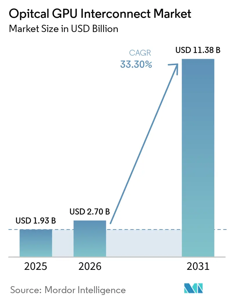
| Market Size (2026) | USD 2.70 Billion |
| Market Size (2031) | USD 11.38 Billion |
| Growth Rate (2026 - 2031) | 33.30% CAGR |
| Fastest Growing Market | Asia-Pacific |
| Largest Market | North America |
| Market Concentration | Medium |
Major Players *Disclaimer: Major Players sorted in no particular order Image © Mordor Intelligence. Reuse requires attribution under CC BY 4.0. | |
Opitcal GPU Interconnect Market Analysis by Mordor Intelligence
The optical GPU interconnect market size is projected to expand from USD 1.93 billion in 2025 and USD 2.70 billion in 2026 to USD 11.38 billion by 2031, registering a CAGR of 33.30% between 2026 and 2031. Growth is tied to a clear shift in large AI clusters, where copper links no longer provide the reach or power profile needed for multi-rack systems. Demand is also moving beyond training clusters because reasoning and inference workloads are beginning to require the same low-latency, high-bandwidth fabric used in training deployments. North America remains the largest revenue base because hyperscalers continue to scale AI infrastructure faster than other regions, while Asia-Pacific is set to post the strongest growth as data center buildouts deepen across major manufacturing and compute hubs. Competition is moving toward tighter vertical control of optics, packaging, and system design, while supply concentration in indium phosphide lasers, standards timing, and thermal design continue to shape adoption speed.
Key Report Takeaways
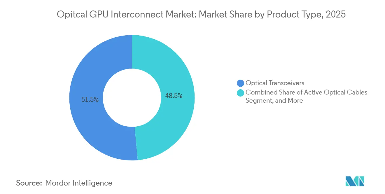
- By product type, Optical Transceivers held 51.47% share in the optical GPU interconnect market in 2025, while Embedded Optical Modules are projected to expand at a 34.29% CAGR through 2031.
- By interconnect level, Board-to-Board and Rack-Level interconnects held 48.84% share in 2025, while Chip-to-Chip is projected to record the highest CAGR at 33.89% through 2031.
- By fiber mode, Multimode Fiber accounted for 57.31% share in 2025, while Single-Mode Fiber is expected to grow at a 33.68% CAGR through 2031.
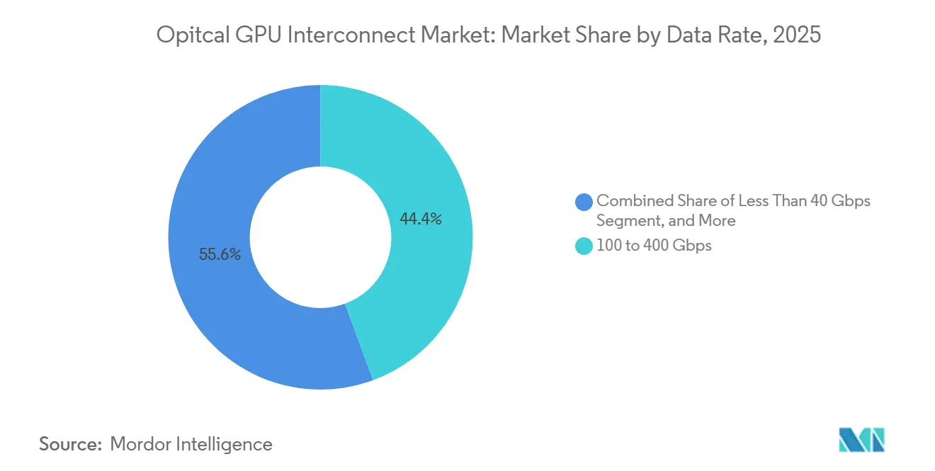
- By data rate, the 100 to 400 Gbps tier captured 44.39% of the market in 2025, while the Above 400 Gbps tier is projected to expand at a 34.13% CAGR through 2031.
- By application, Data Communication accounted for 64.58% of the optical graphics processing unit (GPU) interconnect market in 2025, and this segment is projected to grow at a 33.71% CAGR through 2031.
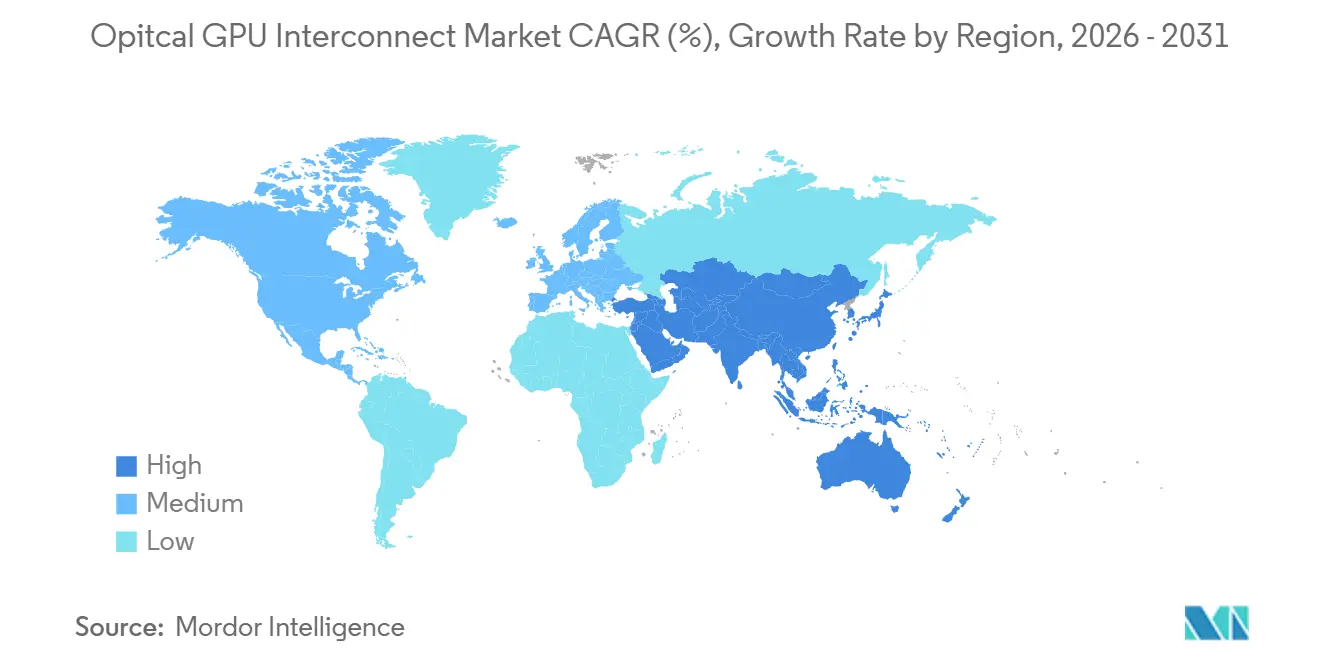
- By geography, North America held 46.32% of the optical GPU interconnect market share in 2025, while Asia-Pacific is projected to post the fastest regional CAGR at 34.27% through 2031.
Note: Market size and forecast figures in this report are generated using Mordor Intelligence’s proprietary estimation framework, updated with the latest available data and insights as of January 2026.
Global Opitcal GPU Interconnect Market Trends and Insights
Driver Impact Analysis*
| Driver | (~) % Impact on CAGR Forecast | Geographic Relevance | Impact Timeline |
|---|---|---|---|
| Rising AI Training and Inference Bandwidth Demand | +6.5% | Global, North America and Asia-Pacific as primary demand centers | Short term (≤ 2 years) |
| Copper Interconnect Power and Reach Limits in GPU Clusters | +5.2% | Global, most acute in high-density GPU clusters in North America and East Asia | Short term (≤ 2 years) |
| Hyperscale Data Center Migration to 800G and 1.6T Architectures | +4.8% | North America core, spillover to Asia-Pacific and Europe | Medium term (2-4 years) |
| Co-Packaged Optics Adoption in Next-Generation GPU Platforms | +4.1% | North America for RandD and first deployments, Asia-Pacific for supply chain ramp | Medium term (2-4 years) |
| Optical I/O Roadmaps From Leading GPU and Switch Vendors | +3.2% | Global, concentrated in North America and Asia-Pacific hyperscale hubs | Medium term (2-4 years) |
| Fiber-Dense Rack and Row Architectures for Disaggregated Compute | +2.6% | Global, strongest adoption in North America, growing across Asia-Pacific and Europe | Long term (≥ 4 years) |
| Source: Mordor Intelligence | |||
Rising AI Training and Inference Bandwidth Demand
AI training clusters expanded from thousands to tens of thousands of GPUs through 2025, and inference systems are now moving in the same direction as reasoning-heavy models become more common. This matters because data movement, not computation alone, now consumes much of the energy inside modern GPU systems. That shift makes interconnect bandwidth a practical limit on cluster design, which directly supports demand across the optical GPU interconnect market. Industry discussions around optical I/O also show that inference workloads increasingly need the same low-latency fabric once associated mainly with training deployments. The result is a broader demand base for optical links, as future spending is no longer tied solely to frontier model training in the optical GPU interconnect market.
Copper Interconnect Power and Reach Limits in GPU Clusters
Copper links face rising signal loss as speed and distance increase, and that physical limit is now affecting system layout in large GPU clusters.[1]NVIDIA, “Scaling AI Factories with Co-Packaged Optics for Better Power Efficiency,” NVIDIA Developer Blog, developer.nvidia.com NVIDIA explained that, in the NVL72 rack, copper runs at NVLink speeds were limited to very short distances, which is why switch placement had to remain tightly constrained inside the chassis. As systems scale from one rack to eight racks, optics move from a useful option to a basic requirement in the optical GPU interconnect market. Research in npj Nanophotonics also found that copper-based scale-up networks cap coherent domains at far lower XPU counts than optical links, which changes how designers think about future cluster size. Power use adds another reason for the shift, because copper-heavy interconnects consume rack power that operators would rather reserve for compute in the optical graphics processing unit (GPU) interconnect market.
Hyperscale Data Center Migration To 800G and 1.6T Architectures
The move from 400G to 800G became the default for new AI-oriented builds in 2026, and 1.6T is already shaping next-round procurement plans across the optical GPU interconnect market. This shift matters because 1.6T is not only a performance upgrade; it is also a supply chain event tied to the slower ramp of 200G-per-lane ecosystems. When supply remains narrow, spending concentrates among qualified module and DSP suppliers, which supports premium pricing in the optical GPU interconnect market. Broadcom’s March 2025 launch of the Sian3 and Sian2M DSP PHY portfolio addressed both 800G and 1.6T transceiver needs and lowered the engineering burden for module vendors preparing for the next speed cycle. That combination of new standards, tighter supply, and synchronized hyperscaler demand keeps the upgrade cycle central to the optical GPU interconnect market.
Co-Packaged Optics Adoption In Next-Generation GPU Platforms
Co-packaged optics entered a more commercial phase in 2026, marking a longer transition away from front-panel pluggables toward near-package optical integration in the optical GPU interconnect market. NVIDIA’s Quantum-X Photonics switch integrated optical engines onto the switch ASIC and combined very high throughput with much lower power use than traditional pluggable designs. Broadcom also showed that CPO had moved beyond pilot scale when its Tomahawk 5-Bailly platform shipped in commercial volume during 2025. Ayar Labs and Wiwynn then demonstrated a scale-up rack with CPO-based optical connectivity, which pushed the concept closer to GPU-adjacent deployment rather than switch-only use. Roadmaps now point to optics moving steadily closer to compute dies, which gives this driver lasting weight in the optical GPU interconnect market.
Restraint Impact Analysis*
| Restraint | (~) % Impact on CAGR Forecast | Geographic Relevance | Impact Timeline |
|---|---|---|---|
| High Cost of Advanced Photonic Packaging and Test | -2.8% | Global, most acute in markets with limited silicon photonics foundry capacity | Short term (≤ 2 years) |
| Thermal Management Constraints in Co-Packaged Designs | -2.1% | Global, especially constraining in high-density AI factory environments | Short term (≤ 2 years) |
| Yield and Reliability Challenges in Heterogeneous Integration | -1.7% | Global, particularly relevant for Asia-Pacific OSAT supply chains | Medium term (2-4 years) |
| Standards and Interoperability Maturity Gaps | -1.3% | Global, enterprise buyers in North America and Europe most exposed | Medium term (2-4 years) |
| Source: Mordor Intelligence | |||
High Cost of Advanced Photonic Packaging and Test
The cost profile of co-packaged optics is much higher than that of standard pluggable modules in the optical GPU interconnect market. Packaging combines CMOS electronics, silicon photonics, and III-V materials, making assembly more difficult and keeping unit economics elevated.[2]Teradyne, “Silicon Photonics Raises New Test Challenges,” Teradyne, teradyne.com Testing adds a second problem because silicon photonics workflows still require several insertions from the wafer stage to the final package, and those flows are not yet optimized for very large volumes. Fiber-to-waveguide alignment also demands precision that is hard to automate fully, so throughput gains do not come as quickly as they did in earlier transceiver cycles. This slows broad enterprise adoption in the optical GPU interconnect market even though hyperscalers are already willing to absorb higher early-stage costs.
Thermal Management Constraints in Co-Packaged Designs
CPO improves power efficiency only by placing optical engines very close to the hot switch ASICs, creating a difficult thermal trade-off in the optical GPU interconnect market. Peer-reviewed packaging work also notes that reliability data on thermal cycling, humidity, and mechanical stress remains limited for these integrated designs. That gap matters because buyers are not deciding on optics alone; they are deciding on chassis cooling, facility upgrades, and long-term maintenance exposure in the optical GPU interconnect market. Conventional air cooling does not fit many of the power densities involved, so liquid-cooled designs become part of the adoption cost rather than an optional enhancement. The challenge is manageable for leading hyperscalers, but it still slows wider deployment in environments that were built around older cooling assumptions.
*Our forecasts treat driver/restraint impacts as directional, not additive. The impact forecasts reflect baseline growth, mix effects, and variable interactions.
Segment Analysis
By Product Type: Pluggable Dominance Giving Way To Integrated Optics
Optical Transceivers held 51.47% of the product type segment in 2025, giving them the leading revenue position in the optical GPU interconnect market. Their lead came from the large installed base of pluggable 400G and 800G modules already supporting deployed AI fabric capacity. That dominance says more about the maturity of current deployments than any long-term limit on optical integration. Pluggables still fit many near-term buildouts because they remain familiar, scalable, and easier to service than newer formats. They also continue to benefit from supply chains that are more established than those for deeply integrated optical packages.
Active Optical Cables stayed relevant for rack-to-rack links where transceiver density mattered less than clean, power-aware short-reach connectivity. Cable Assemblies and Optical Connectors also remained essential because the optical GPU interconnect market depends on physical fiber distribution, patching, and cluster-level installation layers, not only on the transceiver module itself. Embedded Optical Modules are projected to grow at a 34.29% CAGR through 2031, which makes them the fastest-growing product group in the optical GPU interconnect market. That growth reflects the shift from front-panel optics to near-package and co-packaged integration as cluster radix expands beyond what copper can handle. A 2025 Nature Photonics study on 3D photonic integration reinforced this direction by showing ultra-low-energy, high-bandwidth interchip links that copper cannot match at similar reach.


By Interconnect Level: Board-Level Volumes Masking A Chip-Level Structural Shift
Board-to-Board and Rack-Level links held 48.84% of the interconnect segment in 2025, making them the largest current layer in the optical GPU interconnect market. Their position reflected the scale of deployed Ethernet and InfiniBand fabrics that still rely on large volumes of rack-connected optical ports. Metro and Long-Haul DCI occupied a secondary position because they provide connectivity between campuses and distributed compute locations rather than the dense internal fabric within each training cluster. Even so, DCI remains relevant because AI compute is spreading across more sites to manage power, cooling, and land limits. The largest revenue pool today still sits where current hyperscale buildouts require the highest port counts.
Chip-to-Chip is projected to record the fastest CAGR of 33.89% through 2031, signaling the next structural shift in the optical GPU interconnect market. Marvell has argued that passive copper traces stop scaling well beyond 100Gbps per lane, which is why optical links begin to matter even inside a rack. Ayar Labs demonstrated this direction at OFC 2025 with a UCIe Optical I/O Retimer Chiplet that delivered 1.024Tbps per optical port and 8.192Tbps per package. Those benchmarks show why chip-level optics are becoming central to long-range product positioning in the optical GPU interconnect market. The optical GPU interconnect industry is now moving from a board-focused scaling model to one that places more value on photonic IC design, chiplet integration, and advanced packaging.
By Fiber Mode: Multimode Installed Base Versus Single-Mode Speed Premium
Multimode Fiber accounted for 57.31% of the fiber mode segment in 2025, maintaining its leading position in the optical GPU interconnect market. That share reflected the large installed base of short-reach multimode infrastructure already used in many data center fabrics. In GPU clusters, OM4 and OM5 remained practical choices for short links because they balanced cost, power, and ease of installation. This kept multimode important for active optical cables and many pluggable deployments inside present rack layouts. Its lead is therefore tied to the current installed base rather than to future performance limits.
Single-Mode Fiber is projected to grow at a 33.68% CAGR through 2031, making it the faster-growing segment of the optical GPU interconnect market. At 800G and 1.6T, lower dispersion and longer reach make single-mode more attractive for inter-rack links, CPO connections, and DCI use. Broadcom’s Sian3 DSP PHY was designed to support both single-mode and multimode options across 800G and 1.6T transceivers, but the design priority around high-speed reach clearly supports more single-mode deployment. NVIDIA’s Quantum-X and Spectrum-X Photonics systems also use single-mode fiber arrays for inter-rack connectivity, anchoring single-mode fiber at the center of next-generation platform design. Research in Nature Communications on 400Gbps per lane silicon photonic transmission further supports the long-term case for single-mode-heavy architectures
By Data Rate: 800G And 1.6T Architectures Reshaping Cluster Design
The 100 to 400 Gbps band accounted for 44.39% of the data rate segment in 2025, making it the largest speed tier in the optical GPU interconnect market. That result reflected the weight of the existing 400G transceiver deployments across current AI fabrics. Lower tiers below 100 Gbps remain, but they are losing strategic importance as new data center projects skip legacy refresh paths. The optical GPU interconnect market still generates substantial revenue from 100G to 400G installations because the installed base is large and replacement cycles are ongoing. Present demand, in other words, still depends on the broad foundation laid by 400G platforms.
Above 400 Gbps is projected to grow at a 34.13% CAGR through 2031, which makes it the fastest-expanding speed tier in the optical GPU interconnect market. That growth comes from the migration to 800G and 1.6T fabrics across hyperscale AI clusters and newer enterprise AI deployments. Procurement patterns in 2026 became more compressed as multiple large buyers moved simultaneously, creating a rare, synchronized demand event across the optical GPU interconnect market. Industry standards are now catching up with commercial deployment needs, with 800GbE already defined and 1.6TbE work continuing through active standards processes within OIF and IEEE. This means many buyers must decide whether to scale 800G now or prepare for a tighter follow-on shift to 1.6T as module availability broadens.
By Application: Data Center Workloads Consolidating Optical Demand
Data Communication held 64.58% of the application segment in 2025 and posted the fastest projected CAGR of 33.71%, making it both the largest and fastest-growing use case in the optical GPU interconnect market. This pattern reflects the scale of AI-driven investment in hyperscale clusters, cloud inference capacity, and enterprise GPU servers. Telecommunication remained smaller because most spending still flowed to internal cluster connectivity rather than to carrier-style network applications. Even so, telecom-linked DCI remains important because distributed GPU campuses require optical paths between facilities. The optical GPU interconnect market, therefore, remains strongly centered on data center workloads rather than on traditional telecom demand.
Google’s use of optical circuit switching in its AI data center architecture demonstrated how inter-rack topology choices can reduce fabric power, thereby widening the commercial role of optics in data communication deployments. Lumentum also disclosed that one optical circuit-switching customer relationship reached the billion-dollar scale, underscoring how concentrated large deals can become in this part of the optical GPU interconnect market. Within the data communication segment, higher-speed intra-cluster links offer stronger price-per-port profiles than older infrastructure, supporting revenue growth even as the cost per bit declines over time. The DCI side is also attracting interest from vendors expanding into AI-specific, shorter-reach coherent offerings, which broadens competition in distributed compute links. This leaves Data Communication with the broadest opportunity set in the optical graphics processing unit (GPU) interconnect market because it spans training clusters, inference clusters, enterprise acceleration, and emerging optical switching use cases.
Geography Analysis
North America held 46.32% of the optical GPU interconnect market in 2025, maintaining its position as the largest regional revenue base. The region led because Google, Microsoft, Meta, Amazon, and other major operators continued to expand AI infrastructure at a scale not matched elsewhere. North American demand also moved early into commercial CPO adoption, with NVIDIA’s Spectrum-X Photonics Ethernet switch entering production in May 2026 and early users including CoreWeave, Lambda, and Oracle Cloud Infrastructure. That early deployment profile gave the region an advantage in both spending and real-world validation across the optical GPU interconnect market. South America remained smaller, but Brazil and Chile grew in importance as hyperscalers expanded their regional data center footprints.
Europe held a meaningful share of the optical GPU interconnect market because Germany, the United Kingdom, and France continued to build AI training and inference capacity. Enterprise buyers in Europe also placed greater emphasis on interoperability, making multi-vendor standards more important to procurement confidence. OIF’s live 800ZR interoperability demonstration at OFC 2026 directly addressed that need in a region where buyers often avoid dependence on a single-vendor stack.[3]OIF, “OIF Demonstrates Industry-Wide Interoperability at Scale at OFC 2026,” OIF, oiforum.com The Middle East and Africa remained earlier-stage, but sovereign AI programs and greenfield builds in Gulf states created room for direct adoption of newer 800G architectures without the burden of large legacy refresh cycles.
Asia-Pacific is projected to grow at a 34.27% CAGR through 2031, which makes it the fastest-growing geography in the optical GPU interconnect market. The region benefits from manufacturing depth, strong optoelectronics capabilities, and a wider base of public and private investment in AI infrastructure. Japan also gained strategic weight as NTT worked on a USD 500 million optical network fund tied to AI data center infrastructure and its broader all-photonics roadmap. South Korea and parts of Southeast Asia are also emerging as secondary hubs, broadening the future revenue map for the optical graphics processing unit (GPU) interconnect market.

Competitive Landscape
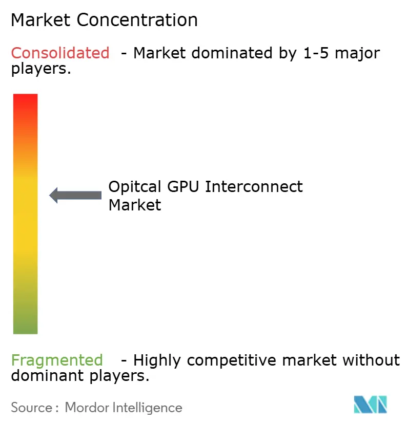
The optical GPU interconnect market remains moderately concentrated, with Broadcom, NVIDIA, Coherent, Lumentum, and Marvell forming the most visible top tier. NVIDIA has pushed the market toward deeper optical integration through its photonics switch roadmap and its public emphasis on solving cluster-scale power and reach constraints with CPO. Broadcom followed a parallel path by commercializing the Tomahawk 5-Bailly CPO switch and extending its roadmap toward higher lane speeds, which signaled that co-packaged optics is a sustained platform direction rather than a one-cycle experiment. Marvell strengthened its position in February 2026 by acquiring Celestial AI, adding Photonic Fabric technology for next-generation scale-up connectivity.[4]Marvell, “Marvell Completes Acquisition of Celestial AI,” Marvell Technology, marvell.com These moves show that leadership in the optical GPU interconnect market increasingly depends on control of system integration rather than on component volume alone.
Another important feature of the optical GPU interconnect market is the open white space around scale-up CPO and optical circuit switching. Scale-up CPO is still early, but it could become one of the most valuable layers once optics move closer to the GPU package. Optical circuit switching is also gaining commercial weight because very large AI clusters need lower-power ways to manage inter-rack connectivity. OIF’s 2026 publications on AI scale-up architectures provided buyers with a more unified framework for comparing CPO, near-package optics, and linear pluggable approaches in the optical GPU interconnect market. That standards work can reduce lock-in risk even as integrated platform vendors seek greater control.
The competitive field also includes challengers such as Ranovus, POET Technologies, and Ayar Labs, each of which is pursuing a different integration path in the optical GPU interconnect market. Ayar Labs has focused on optical chiplets and scale-up fabrics, while POET has emphasized wafer-level photonic integration and optical engine design. Ranovus has pursued monolithic electro-optic integration, offering a different path from the hybrid packaging strategies used by several larger players. This keeps innovation pressure high even as larger vendors consolidate critical assets. The net result is a market where no single player dominates every layer, but where the value of vertical integration is rising quickly across the optical GPU interconnect market.
Opitcal GPU Interconnect Industry Leaders
Broadcom Inc.
NVIDIA Corporation
Intel Corporation
Marvell Technology, Inc.
Coherent Corp.
- *Disclaimer: Major Players sorted in no particular order

Recent Industry Developments
- June 2026: Source Photonics Holdings, wholly owned subsidiary of Dongshan Precision, announced a USD 1.2 billion capacity expansion program for high-end optical chips and high-speed modules targeting 800G and 1.6T AI server interconnect applications at facilities in Changzhou and other locations.
- May 2026: NVIDIA's Spectrum-X Ethernet Photonics CPO switch, described as the world's first CPO Ethernet switch built on 200G SerDes, entered production at Computex 2026. CoreWeave, Lambda, and Oracle Cloud Infrastructure were named among the initial enterprise adopters, marking CPO's first commercial scale-out Ethernet deployment.
- March 2026: Ayar Labs raised USD 500 million in a Series E round at a USD 3.75 billion valuation, with NVIDIA, AMD, and MediaTek as strategic participants, bringing total outside funding to USD 870 million. Ayar Labs subsequently joined NVIDIA's NVLink Fusion program to bring CPO optical chiplets to rack-scale AI infrastructure.
- February 2026: Marvell Technology completed its acquisition of Celestial AI for USD 3.25 billion, with up to USD 5.5 billion in potential milestone payments, adding Photonic Fabric optical interconnect technology to Marvell's portfolio and positioning the company to address scale-up connectivity requirements for next-generation AI and cloud data centers.


Global Opitcal GPU Interconnect Market Report Scope
The Optical GPU Interconnect Market comprises optical communication technologies, components, and systems that enable high-speed data transfer between graphics processing units (GPUs), accelerators, servers, storage systems, and networking infrastructure within AI clusters, high-performance computing (HPC) environments, cloud data centers, and telecommunications networks. Optical GPU interconnects use fiber-optic transmission to overcome the bandwidth, latency, power consumption, and signal-integrity limitations of traditional electrical interconnects, enabling scalable communication across increasingly dense and distributed compute architectures.
The Optical GPU Interconnect Market report is Segmented by Product Type (Optical Transceivers, Active Optical Cables, Embedded Optical Modules, Cable Assemblies, and Optical Connectors), Interconnect Level (Chip-to-Chip, Board-to-Board and Rack-Level, and Metro and Long-Haul DCI), Fiber Mode (Single-Mode Fiber, and Multimode Fiber), Data Rate (Less Than 40 Gbps, 40 to 100 Gbps, 100 to 400 Gbps, and Above 400 Gbps), Application (Data Communication, and Telecommunication), and Geography (North America, Europe, Asia-Pacific, South America, and Middle East and Africa). The Market Forecasts are Provided in Terms of Value (USD).
| Optical Transceivers |
| Active Optical Cables |
| Embedded Optical Modules |
| Cable Assemblies |
| Optical Connectors |
| Chip-to-Chip |
| Board-to-Board and Rack-Level |
| Metro and Long-Haul DCI |
| Single-Mode Fiber |
| Multimode Fiber |
| Less Than 40 Gbps |
| 40 to 100 Gbps |
| 100 to 400 Gbps |
| Above 400 Gbps |
| Data Communication |
| Telecommunication |
| North America | United States |
| Canada | |
| Mexico | |
| Europe | Germany |
| United Kingdom | |
| France | |
| Italy | |
| Rest of Europe | |
| Asia-Pacific | China |
| Japan | |
| South Korea | |
| India | |
| Southeast Asia | |
| Rest of Asia-Pacific | |
| South America | |
| Middle East and Africa |
| By Product Type | Optical Transceivers | |
| Active Optical Cables | ||
| Embedded Optical Modules | ||
| Cable Assemblies | ||
| Optical Connectors | ||
| By Interconnect Level | Chip-to-Chip | |
| Board-to-Board and Rack-Level | ||
| Metro and Long-Haul DCI | ||
| By Fiber Mode | Single-Mode Fiber | |
| Multimode Fiber | ||
| By Data Rate | Less Than 40 Gbps | |
| 40 to 100 Gbps | ||
| 100 to 400 Gbps | ||
| Above 400 Gbps | ||
| By Application | Data Communication | |
| Telecommunication | ||
| By Geography | North America | United States |
| Canada | ||
| Mexico | ||
| Europe | Germany | |
| United Kingdom | ||
| France | ||
| Italy | ||
| Rest of Europe | ||
| Asia-Pacific | China | |
| Japan | ||
| South Korea | ||
| India | ||
| Southeast Asia | ||
| Rest of Asia-Pacific | ||
| South America | ||
| Middle East and Africa | ||


Key Questions Answered in the Report
What is the current size of the optical GPU interconnect market?
The optical GPU interconnect market was valued at USD 1.93 billion in 2025 and is valued at USD 2.7 billion in 2026. It is projected to reach USD 11.38 billion by 2031 at a 33.30% CAGR.
Why are optical links replacing copper in large GPU clusters?
Copper now faces practical reach and power limits in multi-rack AI systems. Optical links support longer distances, lower power draw in scaled fabrics, and better fit for 800G and 1.6T architectures.
Which product category leads revenue today?
Optical Transceivers led product revenue with 51.47% share in 2025 because pluggable 400G and 800G modules still support most deployed AI fabric capacity.
Which segment is growing the fastest by application?
Data Communication is the fastest-growing application with a projected 33.71% CAGR through 2031. It also held the largest application share at 64.58% in 2025.
Which region offers the strongest growth outlook?
Asia-Pacific has the strongest growth outlook with a projected 34.27% CAGR through 2031, while North America remained the largest region with 46.32% share in 2025.
What are the main risks affecting adoption?
The main constraints are high photonic packaging and test costs, thermal complexity in co-packaged designs, yield and reliability issues in heterogeneous integration, and standards timing across next-generation interfaces.
Page last updated on:


