Chiplet-Based GPU Market Size and Share
Market Overview
| Study Period | 2020 - 2031 |
|---|---|
| Market Size (2026) | USD 3.40 Billion |
| Market Size (2031) | USD 13.75 Billion |
| Growth Rate (2026 - 2031) | 32.30% CAGR |
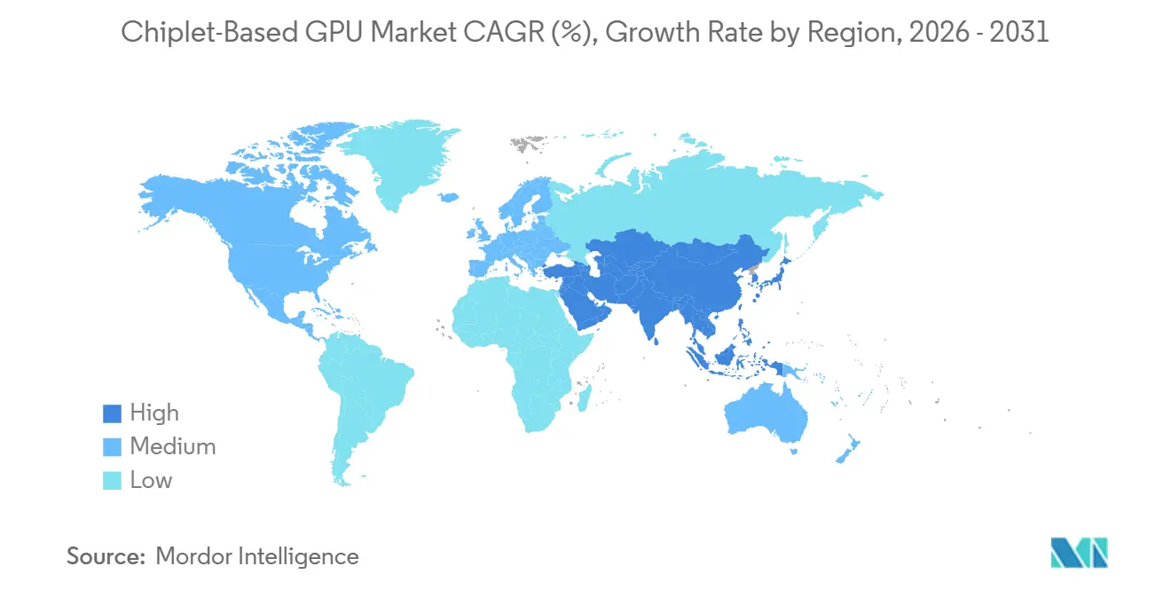
| Fastest Growing Market | Asia-Pacific |
| Largest Market | North America |
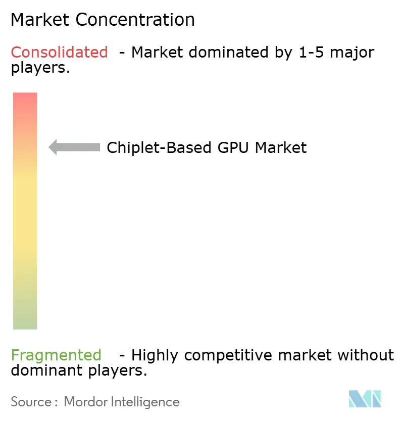
| Market Concentration | High |
Major Players *Disclaimer: Major Players sorted in no particular order Image © Mordor Intelligence. Reuse requires attribution under CC BY 4.0. | |
Chiplet-Based GPU Market Analysis by Mordor Intelligence
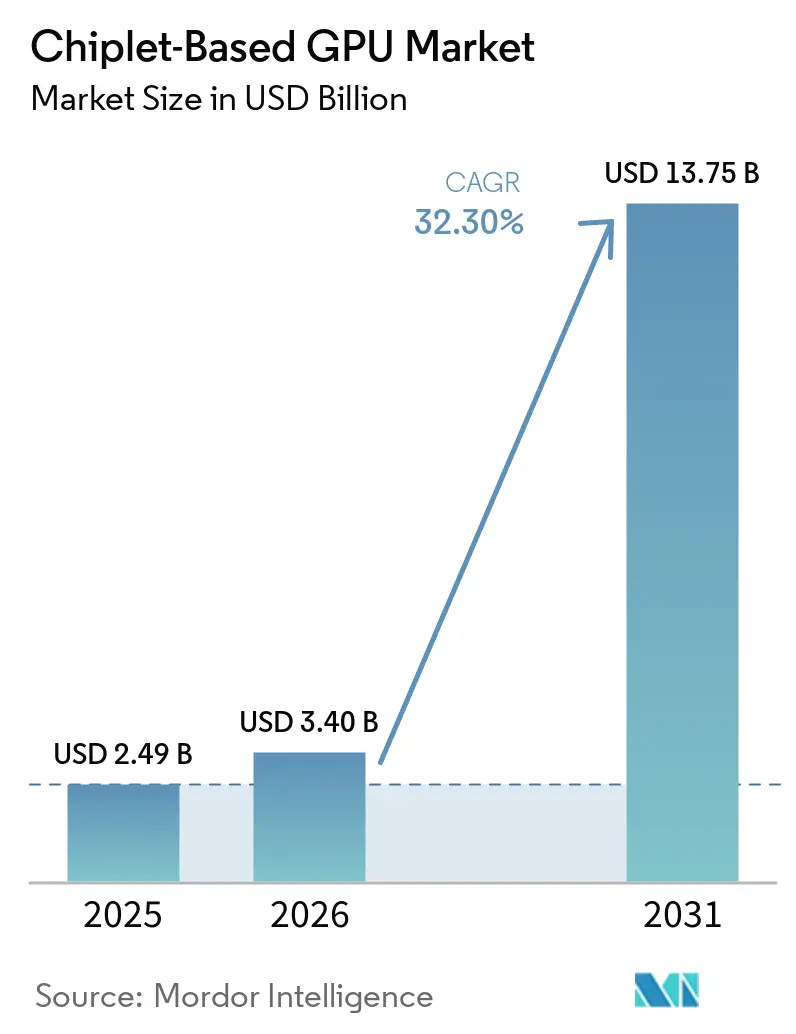
The chiplet-based GPU market size is projected to be USD 2.49 billion in 2025, USD 3.4 billion in 2026, and reach USD 13.75 billion by 2031, growing at a CAGR of 32.30% from 2026 to 2031. Growth in the chiplet-based GPU market reflects a structural shift in GPU design, because reticle-size limits and rising non-recurring engineering costs at advanced nodes are making monolithic scaling less practical for leading programs. Larger AI training workloads, tighter integration with high-bandwidth memory, and the growing maturity of advanced packaging across major foundries and outsourced assembly partners are also reinforcing demand. Sovereign AI programs, hyperscaler capital spending, and wider support for open die-to-die standards are expanding the commercial base of the chiplet-based GPU market beyond a narrow set of internal hyperscale projects. Competition remains concentrated around a small group of leading GPU roadmaps, but new entry points are opening in interconnect, optical I/O, packaging, and test flows. Thermal design, power delivery, and interoperability still slow execution in the chiplet-based GPU market, but these same constraints are directing investment toward 3D stacking, open standards, and co-packaged optics.
Key Report Takeaways
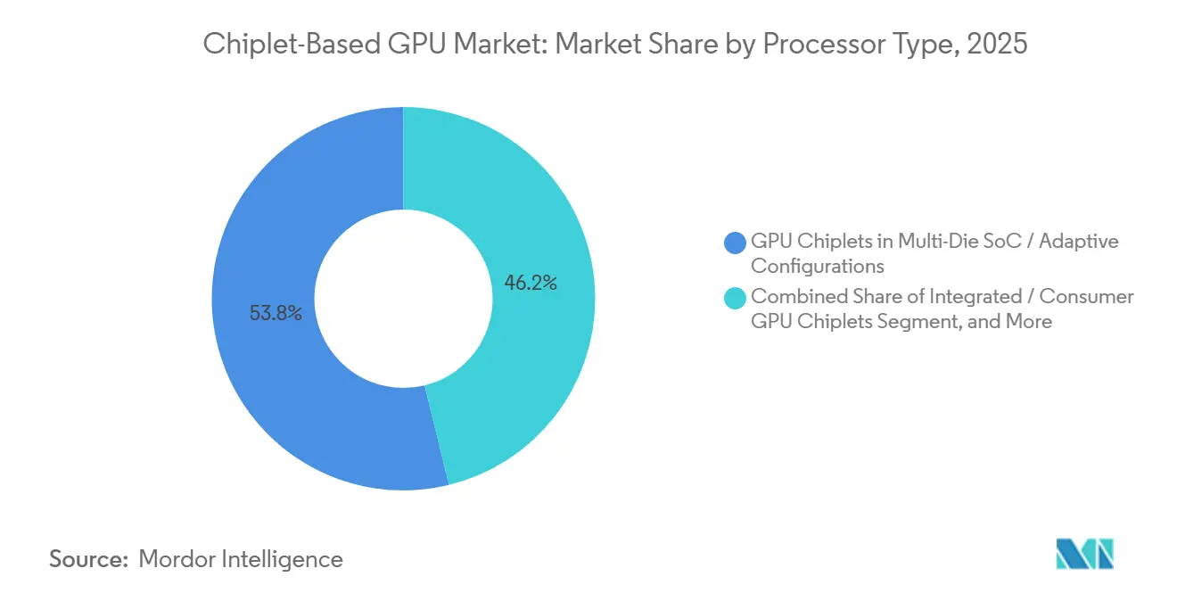
- By processor type, GPU chiplets in multi-die SoCs and adaptive configurations held a 53.81% share in the chiplet-based GPU market in 2025, while AI-accelerator GPU chiplets and heterogeneous GPU modules are projected to expand at a 33.28% CAGR through 2031.
- By packaging technology, 2.5D interposer and bridge-based packaging accounted for 47.48% of the chiplet-based GPU market in 2025, while 3D-stacked and hybrid-bonded packaging is projected to grow at a 33.19% CAGR through 2031.
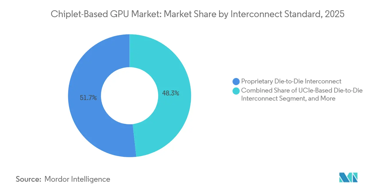
- By interconnect standard, proprietary die-to-die interconnects held a 51.74% share in 2025, while UCIe-based die-to-die interconnects are projected to expand at a 32.88% CAGR through 2031.
- By end-user industry, data centers and cloud computing accounted for 46.32% share of the chiplet-based GPU market size in 2025, while industrial and edge AI are projected to grow at a 33.91% CAGR through 2031.
- By geography, North America held 46.94% of the chiplet-based graphics processing unit (GPU) market share in 2025, while the Middle East and Africa are projected to record the highest CAGR at 32.98% through 2031.
Note: Market size and forecast figures in this report are generated using Mordor Intelligence’s proprietary estimation framework, updated with the latest available data and insights as of January 2026.
Global Chiplet-Based GPU Market Trends and Insights
Driver Impact Analysis*
| Driver | (~) % Impact on CAGR Forecast | Geographic Relevance | Impact Timeline |
|---|---|---|---|
| AI aznd HPC Reticle-Limit Escape | +5.8% | Global, with highest concentration in North America and Asia-Pacific | Short term (≤ 2 years) |
| HBM-Centered 2.5D and 3D Package Adoption | +5.2% | Global, led by Asia-Pacific | Short term (≤ 2 years) |
| Advanced-Node NRE Reduction Through IP Reuse | +4.1% | North America and Europe, with growing Asia-Pacific contribution | Medium term (2-4 years) |
| 5G, Cloud, and Networking Demand For Disaggregated Silicon | +3.6% | Global, with spillover into the Middle East and Africa and South America | Medium term (2-4 years) |
| Optical I/O Chiplets for Rack-Scale AI Scale-Up | +3.2% | North America and Asia-Pacific core, with early Middle East and Africa adoption | Long term (≥ 4 years) |
| KGD Testing and UCIe Alliances De-Risk Merchant Chiplets | +2.8% | Global, with North America and Asia-Pacific core | Medium term (2-4 years) |
| Source: Mordor Intelligence | |||
AI and HPC Reticle-Limit Escape
The reticle-size limit has become a direct design constraint in the chiplet-based GPU market, as leading AI training systems can no longer rely solely on monolithic scaling. NVIDIA moved this issue into commercial production with Vera Rubin, which combines 2 reticle-sized compute chiplets with 8 HBM4 stacks, and is scheduled for volume shipment in the second half of 2026.[1]NVIDIA Corporation, “NVIDIA Vera Rubin POD, Seven Chips, Five Rack-Scale Systems, One AI Supercomputer,” NVIDIA Technical Blog, nvidia.com Intel Foundry also stated that the EMIB 2.5D interconnect is engineered to support more than 8 times the reticle size in 2026 and 12 times by 2028, indicating that package-level scaling is replacing die-level scaling in advanced GPU programs. This change favors companies that can partition compute, memory, and I/O across several dies without losing performance, yield discipline, or software alignment. AMD reinforced that direction when it linked Helios deployments beginning in the second half of 2026 to MI450X chiplet GPUs, which confirms that reticle escape is now part of production platform planning rather than an experimental architecture path.
HBM-Centered 2.5D and 3D Package Adoption
HBM integration has become a baseline requirement for competitive AI accelerators, making 2.5D and 3D packaging among the strongest growth engines in the chiplet-based GPU market. TSMC said its CoWoS capacity expanded from 15,000 wafers per month at the end of 2023 to 70,000-80,000 wafers per month at the end of 2025, and it is targeting 120,000-130,000 wafers per month by the end of 2026. Even with that ramp, major GPU programs still depend on early allocation of interposer and HBM integration capacity, which keeps packaging access strategically important for launch timing and customer fulfillment. Samsung also highlighted advanced heterogeneous integration and hybrid copper bonding as part of its roadmap for dense multi-die structures, which supports the move toward tighter GPU and memory coupling. The result is a chiplet-based GPU market where packaging readiness now shapes product competitiveness almost as much as logic-node access.
Advanced-Node NRE Reduction Through IP Reuse
The chiplet-based GPU market also benefits from lower redevelopment costs when vendors reuse validated blocks across multiple product generations. Stable I/O dies, SerDes structures, and memory controllers can remain in place while only the compute chiplet moves to a new node, reducing the full-system requalification required in each cycle. This reuse model matters more as process nodes become costlier, because it gives vendors a way to preserve platform continuity while still improving compute density where it matters most. Cadence said UCIe 3.0 support is now integrated into its physical implementation flow, reducing part of the design overhead associated with modular die integration. As those workflows mature, the economic case for the chiplet-based graphics processing unit (GPU) market extends beyond the largest hyperscaler programs and into a wider set of enterprise and specialized accelerator designs.
5G, Cloud, and Networking Demand For Disaggregated Silicon
Demand from cloud infrastructure, telecom processing, and distributed AI is driving the adoption of modular GPU designs in the chiplet-based GPU market. NVIDIA's 2026 platform direction continues to link performance gains to larger rack-scale systems, higher memory bandwidth, and multi-die configurations, which support broader use of disaggregated compute building blocks. In these environments, chiplets make it easier to tune compute, memory, and connectivity for different rack, edge, and network requirements without redesigning a full monolithic device. The same flexibility matters in industrial and telecom settings, where power limits, form factor, latency, and environmental conditions vary more than in centralized training clusters. As deployment patterns spread beyond hyperscale data centers, the addressable market for chiplet-based GPUs continues to expand.
Restraint Impact Analysis*
| Restraint | (~) % Impact on CAGR Forecast | Geographic Relevance | Impact Timeline |
|---|---|---|---|
| Thermal and Power-Delivery Bottlenecks in Dense GPU Packages | -3.8% | Global, most acute in North America and Asia-Pacific | Short term (≤ 2 years) |
| Immature Cross-Vendor Interoperability and IP Liability | -2.9% | Global | Medium term (2-4 years) |
| Yield Compounding and Test-Cost Inflation In KGD Flows | -2.4% | Asia-Pacific core, with spillover into North America | Medium term (2-4 years) |
| CoWoS, Interposer, Substrate, and Optical-Packaging Bottlenecks | -2.1% | Asia-Pacific core, with global spillover | Short term (≤ 2 years) |
| Source: Mordor Intelligence | |||
Thermal and Power-Delivery Bottlenecks In Dense GPU Packages
Thermal and power-delivery limits remain the hardest execution problem in the chiplet-based GPU market, especially as AI package power rises beyond levels that conventional air cooling can sustain efficiently. Semiconductor Engineering reported that AI accelerator packages integrating 4 or more HBM stacks are now pushing past 1 kW per device, which raises cooling, power integrity, and long-run reliability demands across the full package stack. The same publication also noted that backside power delivery can increase local hotspot temperatures relative to frontside approaches, adding another layer of trade-offs in dense AI package design. These limits do not prevent adoption, but they can delay ramps, increase integration costs, and reduce the number of teams that can execute advanced thermal co-design successfully. That is why performance gains in the chiplet-based GPU market are becoming more dependent on cooling architecture, power planning, and package layout working together from the start.
Immature Cross-Vendor Interoperability and IP Liability
Cross-vendor interoperability remains immature in the chiplet-based GPU market, even as support for open die-to-die standards improves quickly. The UCIe Consortium released version 3.0 in August 2025, with 64GT/s data rates, 3D packaging support, a longer sideband channel, and standardized firmware download, thereby strengthening the technical foundation for multi-vendor integration. Even so, proprietary fabrics still lead current revenue because they offer known bandwidth, latency, validation practices, and accountability within tightly controlled ecosystems. Synopsys taped out 64Gbps UCIe IP on 2nm technology in 2025, and Cadence added UCIe 3.0 implementation support, but commercial liability and design responsibility across mixed-vendor packages are still evolving.[2]Cadence Design Systems, “3D-IC Test and Reliability, KGD Strategies, Access Architecture, and Failure Mode,” Cadence Community Blog, cadence.com Until those workflows mature, some system builders will continue to favor vertically controlled chiplet stacks over more open combinations.
*Our forecasts treat driver/restraint impacts as directional, not additive. The impact forecasts reflect baseline growth, mix effects, and variable interactions.
Segment Analysis
By Processor Type: AI Accelerator Modules Lift The Growth Ceiling
GPU chiplets in multi-die SoCs and adaptive configurations drove processor-type demand, with 53.81% of the chiplet-based GPU market share in 2025. AI accelerator GPU chiplets and heterogeneous GPU modules are projected to grow at a 33.28% CAGR through 2031, making them the fastest-expanding processor type in the chiplet-based GPU market. That acceleration follows the move toward training systems that require reticle escape, higher memory bandwidth, and modular scaling rather than a larger monolithic die. NVIDIA's Vera Rubin platform illustrates this shift with a dual-compute chiplet architecture and 8 HBM4 stacks, in a commercial product cycle aimed at second-half 2026 volume shipments.
Multi-die SoC configurations kept the broadest base because they fit enterprise, automotive, and consumer programs that need modular compute without the full cost profile of frontier AI accelerators. The processor mix is also shifting because reusable chiplets let vendors carry forward validated I/O and memory structures while updating only the compute die for a new node. That matters in programs with longer design cycles, where qualification discipline and platform continuity are as important as absolute peak throughput. AMD's 2026 infrastructure planning around MI450X inside the Helios system shows how processor choices are now being tied directly to rack-level deployment models in the chiplet-based GPU market


By Packaging Technology: 2.5D Leads While 3D Gains Ground
2.5D interposer and bridge-based packaging accounted for 47.48% of the chiplet-based GPU market in 2025, maintaining its lead as the leading packaging approach. This segment stayed ahead because CoWoS remains the practical production path for leading AI GPU programs that need high-bandwidth memory and dense die-to-die routing. TSMC's published roadmap shows a sharp ramp in CoWoS capacity through 2026, confirming how central this platform has become to advanced GPU commercialization. AMD also added another supply-side option in May 2026 by qualifying a 2.5D panel-based Elevated Fanout Bridge interconnect with PTI, which could ease pressure on conventional wafer-based flows if production execution remains stable.
3D-stacked and hybrid-bonded packaging is projected to grow at a 33.19% CAGR through 2031, making it the fastest-growing packaging segment in the chiplet-based GPU market. The appeal of 3D integration stems from shorter interconnect paths, tighter memory coupling, and the ability to increase bandwidth without expanding the package footprint. Samsung stated that its advanced heterogeneous integration roadmap includes hybrid copper bonding for dense multi-die structures, which supports the next stage of package scaling. Over the forecast period, 2.5D should remain the volume leader while 3D packaging gains share in programs where bandwidth density and system efficiency justify higher integration complexity.
By Interconnect Standard: Open UCIe Momentum Builds Against Closed Ecosystems
Proprietary die-to-die interconnects held a 51.74% share in 2025, keeping closed ecosystems in the lead across current high-end deployments. UCIe-based die-to-die interconnect is projected to grow at a 32.88% CAGR through 2031, making it the fastest-growing interconnect segment in the chiplet-based GPU market. The current balance reflects a clear tradeoff, because proprietary fabrics still provide proven bandwidth, latency, and validation behavior inside tightly managed platforms. The UCIe Consortium strengthened the open alternative in August 2025 when it released version 3.0 with 64GT/s data rates, 3D packaging support, a 100mm sideband channel, and standardized firmware download.
Open standards are also becoming easier to use as the supporting design ecosystem improves for implementation, verification, and IP packaging. Synopsys completed a 64 Gbps UCIe IP tape-out on 2nm technology in 2025, demonstrating a production-ready path for advanced-node modular designs. Cadence added UCIe 3.0 support to its physical implementation flow, reducing practical barriers for teams building multi-die systems. Even so, migration from proprietary fabrics will be gradual because interconnect choices are locked early and remain tied to software, validation, and full-platform deployment models.
By End-User Industry: Edge AI Expands The Demand Base
Data centers and cloud computing accounted for 46.32% of the chiplet-based GPU market in 2025, making them the largest end-user segment. Industrial and edge AI is projected to grow at a 33.91% CAGR through 2031, making it the fastest-growing end-user segment in the chiplet-based GPU market. Hyperscaler demand still sets the volume foundation, because large AI clusters continue to absorb leading chiplet GPUs with the highest memory and packaging requirements. NVIDIA's 2026 roadmap keeps that center of gravity in place through Blackwell and Vera Rubin deployments across large-scale AI infrastructure.
Edge and industrial use is rising because chiplet architectures let vendors size compute, memory, and I/O for power-constrained inference systems, rather than forcing a single design across every deployment. This makes the model relevant for factory automation, smart cameras, telecom edge nodes, and private network infrastructure that operate with tighter thermal and form-factor limits. The automotive and mobility path remains more gradual because reliability certification and functional safety requirements add qualification work to chiplet integration. The UCIe Consortium included automotive-focused reliability and health-monitoring features in version 1.1, enabling broader use of modular die architectures beyond centralized data center systems. Tenstorrent's Open Chiplet Atlas ecosystem also shows that the wider accelerator base is testing modular supply models beyond the traditional GPU lineage
Geography Analysis
North America accounted for 46.94% of the chiplet-based GPU market share in 2025, making it the largest regional market. The region benefits from the concentration of NVIDIA, AMD, Intel, hyperscalers, EDA vendors, and advanced packaging partners across the United States. NVIDIA's September 2025 collaboration with Intel on custom data center and PC products shows how core architecture decisions and ecosystem alliances are still set in North America.[3]NVIDIA Corporation, “NVIDIA and Intel to Develop AI Infrastructure and Personal Computing Products,” NVIDIA Newsroom, nvidia.com Intel also keeps the region strong in packaging and foundry technology through EMIB and Foveros roadmaps aimed at high-performance AI systems.
Asia-Pacific remained the second-largest region and the main production base for the chiplet-based GPU market in 2025. The region concentrates CoWoS and SoIC capacity at TSMC, advanced heterogeneous integration programs at Samsung, major HBM supply chains, and large OSAT operations. TSMC's CoWoS roadmap and Samsung's advanced packaging roadmap show why Asia-Pacific continues to control the manufacturing side of advanced GPU assembly. AMD reinforced that dependence in May 2026, when it announced more than USD 10 billion in investments in the Taiwan ecosystem, tied to packaging, bridge interconnect development, and Helios production. This leaves Asia-Pacific at the center of near-term execution risk and near-term opportunity for the chiplet-based GPU market.
The Middle East and Africa are projected to expand at a 32.98% CAGR through 2031, making it the fastest-growing regional segment in the chiplet-based graphics processing unit (GPU) market. Growth in this region is tied to sovereign AI programs, data center build-outs, and broader efforts to secure local access to advanced compute infrastructure. Europe remains important through supercomputing demand, automotive computing programs, and materials compliance requirements that affect packaging choices. South America is still earlier in adoption, with demand centered more on access to cloud-based AI compute than on direct procurement of chiplet GPU hardware. Together, these regional patterns show a market led by North American design control, Asia-Pacific manufacturing depth, and faster new demand formation in the Middle East and Africa.

Competitive Landscape
The chiplet-based GPU market is concentrated at the compute-roadmap level, as a small group of companies controls the most advanced GPU architectures and platform ecosystems. NVIDIA, AMD, and Intel set the pace in product definition, while TSMC remains the critical manufacturing partner for high-end interposer and advanced packaging capacity. NVIDIA's strategy centers on vertical integration across GPU design, NVLink fabric, and software, which helps it align architecture decisions to a broader platform model. AMD has leaned into open software positioning and chiplet cost structure, while tying its 2026 Taiwan investment program to future packaging scale and rack-level deployment. Intel continues to play a dual role as a product company and a foundry platform provider through EMIB, Foveros, and UCIe participation.[4]Intel Foundry, “Accelerating HPC and AI with Advanced Process and Packaging Technologies,” Intel Foundry HPC-AI Brief, intel.com
Competition is more open in the interconnect, optical I/O, and merchant chiplet layers, where no single company holds the same degree of ecosystem control. The UCIe Consortium's 2025 version 3.0 release strengthened the open-standards path and enabled more vendors to adopt a common framework for die-to-die communication. Tenstorrent used that opening to launch its Open Chiplet Atlas ecosystem with more than 50 partners, signaling growing interest in modular supply chains for accelerator chiplets. Ayar Labs and Alchip also formed a strategic partnership in September 2025 to scale co-packaged optics for AI infrastructure using TSMC's CoWoS and SoIC platforms. These moves show that challengers are not competing only on compute silicon; they are also competing on the links that connect larger AI systems.
Strategic control in the chiplet-based graphics processing unit (GPU) market now depends on software, packaging access, interconnect choice, and deployment model rather than on transistor scaling alone. That is why leading companies are making moves across alliances, supply chain commitments, and standards participation simultaneously. The result is a market with limited top-tier architecture leadership but a broader set of opportunities for firms that solve packaging density, optical scale-up, or interoperable die integration. This structure supports strong concentration at the center of the market while still leaving room for specialized entrants around the edges.
Chiplet-Based GPU Industry Leaders
NVIDIA Corporation
Advanced Micro Devices, Inc.
Intel Corporation
Taiwan Semiconductor Manufacturing Company Limited
Samsung Electronics Co., Ltd.
- *Disclaimer: Major Players sorted in no particular order

Recent Industry Developments
- May 2026: AMD announced more than USD 10 billion in Taiwan ecosystem investments, qualifying the industry's first 2.5D panel-based Elevated Fanout Bridge interconnect with PTI and initiating Helios rack-scale platform deployment featuring MI450X chiplet GPUs in multi-gigawatt deployments beginning in the second half of 2026.
- March 2026: NVIDIA launched the Vera Rubin NVL72 platform at GTC 2026, integrating 72 Rubin GPUs built on dual-reticle-sized compute chiplets with HBM4 memory, targeting full production shipment in the second half of 2026 with a combined Blackwell and Vera Rubin order pipeline spanning multiple hyperscaler generations.
- September 2025: NVIDIA and Intel announced a landmark collaboration to jointly develop multiple generations of custom data center and PC products, with NVIDIA investing USD 5 billion in Intel common stock. Intel will produce x86 SoCs integrating NVIDIA RTX GPU chiplets and custom Xeon CPUs with NVLink integration for AI infrastructure.
- September 2025: Ayar Labs and Alchip Technologies announced a strategic partnership to accelerate AI scale-up infrastructure using co-packaged optics, leveraging TSMC's CoWoS and SoIC packaging platforms, targeting commercial CPO deployment in GPU-scale AI accelerators from 2026 through 2028.


Global Chiplet-Based GPU Market Report Scope
The Chiplet-Based GPU Market comprises graphics processing units (GPUs) designed using a chiplet architecture, in which multiple smaller semiconductor dies are integrated into a single package to form a unified computing platform. Unlike traditional monolithic GPU designs, chiplet-based GPUs leverage modular die-to-die integration technologies to improve scalability, manufacturing yields, performance efficiency, design flexibility, and cost optimization. These architectures enable GPU manufacturers to combine compute, memory, cache, input/output, and specialized accelerator functions across multiple interconnected dies using advanced packaging and interconnect technologies.
The Chiplet-Based GPU Market is Segmented by Processor Type (Discrete / High-Performance Compute GPU Chiplets, Integrated / Consumer GPU Chiplets, AI Accelerator GPU Chiplets / Heterogeneous GPU Modules, GPU Chiplets in Multi-Die SoC / Adaptive Configurations, and Other Chiplet-Based GPU Variants), Packaging Technology (2.5D Interposer and Bridge-Based Packaging, 3D Stacked and Hybrid-Bonded Packaging, Fan-Out and RDL-Based Advanced Packaging, Organic Substrate-Based Multi-Die Packaging, and Other Packaging Technologies), Interconnect Standard (UCIe-Based Die-to-Die Interconnect, Proprietary Die-to-Die Interconnect, and Hybrid Open-Standard and Proprietary Architectures), End-user Industry (Data Centers and Cloud Computing, High-Performance Computing, Consumer Computing, Automotive and Mobility, Telecommunications and Networking, Industrial and Edge AI, Aerospace and Defense, and Other End-user Industries), and Geography (North America, Europe, Asia-Pacific, South America, and Middle East and Africa). The Market Forecasts are Provided in Terms of Value (USD).
| Discrete / High-Performance Compute GPU Chiplets |
| Integrated / Consumer GPU Chiplets |
| AI Accelerator GPU Chiplets / Heterogeneous GPU Modules |
| GPU Chiplets in Multi-Die SoC / Adaptive Configurations |
| Other Chiplet-Based GPU Variants |
| 2.5D Interposer and Bridge-Based Packaging |
| 3D Stacked and Hybrid-Bonded Packaging |
| Fan-Out and RDL-Based Advanced Packaging |
| Organic Substrate-Based Multi-Die Packaging |
| Other Packaging Technologies |
| UCIe-Based Die-to-Die Interconnect |
| Proprietary Die-to-Die Interconnect |
| Hybrid Open-Standard and Proprietary Architectures |
| Data Centers and Cloud Computing |
| High-Performance Computing |
| Consumer Computing |
| Automotive and Mobility |
| Telecommunications and Networking |
| Industrial and Edge AI |
| Aerospace and Defense |
| Other End-user Industries |
| North America | United States |
| Canada | |
| Mexico | |
| Europe | Germany |
| United Kingdom | |
| France | |
| Italy | |
| Rest of Europe | |
| Asia-Pacific | China |
| Japan | |
| South Korea | |
| India | |
| Southeast Asia | |
| Rest of Asia-Pacific | |
| South America | |
| Middle East and Africa |
| By Processor Type | Discrete / High-Performance Compute GPU Chiplets | |
| Integrated / Consumer GPU Chiplets | ||
| AI Accelerator GPU Chiplets / Heterogeneous GPU Modules | ||
| GPU Chiplets in Multi-Die SoC / Adaptive Configurations | ||
| Other Chiplet-Based GPU Variants | ||
| By Packaging Technology | 2.5D Interposer and Bridge-Based Packaging | |
| 3D Stacked and Hybrid-Bonded Packaging | ||
| Fan-Out and RDL-Based Advanced Packaging | ||
| Organic Substrate-Based Multi-Die Packaging | ||
| Other Packaging Technologies | ||
| By Interconnect Standard | UCIe-Based Die-to-Die Interconnect | |
| Proprietary Die-to-Die Interconnect | ||
| Hybrid Open-Standard and Proprietary Architectures | ||
| By End-user Industry | Data Centers and Cloud Computing | |
| High-Performance Computing | ||
| Consumer Computing | ||
| Automotive and Mobility | ||
| Telecommunications and Networking | ||
| Industrial and Edge AI | ||
| Aerospace and Defense | ||
| Other End-user Industries | ||
| By Geography | North America | United States |
| Canada | ||
| Mexico | ||
| Europe | Germany | |
| United Kingdom | ||
| France | ||
| Italy | ||
| Rest of Europe | ||
| Asia-Pacific | China | |
| Japan | ||
| South Korea | ||
| India | ||
| Southeast Asia | ||
| Rest of Asia-Pacific | ||
| South America | ||
| Middle East and Africa | ||


Key Questions Answered in the Report
What is the current and forecast value of chiplet-based GPUs?
The chiplet-based GPU market size was USD 2.49 billion in 2025, reached USD 3.4 billion in 2026, and is forecast to reach USD 13.75 billion by 2031 at a 32.30% CAGR.
Why are chiplets becoming important in GPU design?
Reticle-size limits, rising advanced-node design costs, and the need for more HBM capacity are making multi-die GPU architectures more practical than larger monolithic designs.
Which processor type is growing fastest in this space?
AI accelerator GPU chiplets and heterogeneous GPU modules are the fastest-growing processor type, with a projected 33.28% CAGR through 2031.
Which packaging approach currently leads revenue?
2.5D interposer and bridge-based packaging led with a 47.48% share in 2025, supported by strong dependence on CoWoS-class packaging for AI GPU deployment.
Which end-user group drives the most demand?
Data centers and cloud computing held the largest end-user share at 46.32% in 2025, reflecting continued hyperscaler demand for advanced AI infrastructure.
Which region is expanding the fastest?
The Middle East and Africa is the fastest-growing region, with a projected 32.98% CAGR through 2031, supported by sovereign AI and data center investment programs.
Page last updated on:


