
GPU Chiplet Packaging Market Size and Share
Market Overview
| Study Period | 2020 - 2031 |
|---|---|
| Market Size (2026) | USD 11.20 Billion |
| Market Size (2031) | USD 29.89 Billion |
| Growth Rate (2026 - 2031) | 21.69 % |
| Fastest Growing Market | North America |
| Largest Market | Asia-Pacific |
| Market Concentration | Medium |
Major Players *Disclaimer: Major Players sorted in no particular order Image © Mordor Intelligence. Reuse requires attribution under CC BY 4.0. | |
GPU Chiplet Packaging Market Analysis by Mordor Intelligence
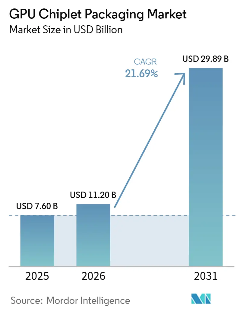
The GPU chiplet packaging market size is expected to increase from USD 7.60 billion in 2025 to USD 11.20 billion in 2026 and reach USD 29.89 billion by 2031, growing at a CAGR of 21.69% over 2026-2031. The GPU chiplet packaging market is expanding because leading GPU roadmaps have moved away from very large monolithic dies and toward multi-die architectures that can support more compute, more memory bandwidth, and better yield management in advanced AI systems. Demand is being pulled most strongly by AI training and inference hardware, where HBM-attached accelerators require 2.5D or 3D integration methods that are now central to product qualification and volume delivery. The GPU chiplet packaging market also reflects a strong regional imbalance, because the most capable foundry, OSAT, and substrate networks remain concentrated in Asia-Pacific even as North America begins to build domestic capacity. Cost remains a meaningful barrier, since the most advanced package designs require more complex assembly flows, stricter thermal control, and longer supplier qualification cycles than simpler package formats. The GPU chiplet packaging market is also developing under a split architecture model, where open chiplet interconnect standards are advancing, but a large share of current high-volume GPU packages still depends on proprietary die-to-die platforms.
Key Report Takeaways
- By GPU platform, Data Center and AI GPUs held 86.11% of the GPU chiplet packaging market in 2025, while the same segment is projected to expand at a 23.21% CAGR through 2031.
- By packaging technology, 2.5D Interposer and Bridge-Based Packaging accounted for 68.33% share in 2025, while 3D Stacked and Hybrid-Bonded Packaging is projected to grow at a 23.62% CAGR through 2031.
- By chiplet function, GPU Compute Chiplets accounted for 42.42% share in 2025, while Memory Chiplets and HBM Integration is expected to expand at a 23.53% CAGR through 2031.
- By application, AI Training and Inference represented 69.12% share in 2025 and is also projected to advance at a 23.32% CAGR through 2031.
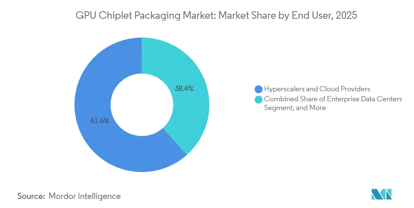
- By end user, Hyperscalers and Cloud Providers held 61.65% share in 2025 and are projected to record a 23.28% CAGR through 2031.
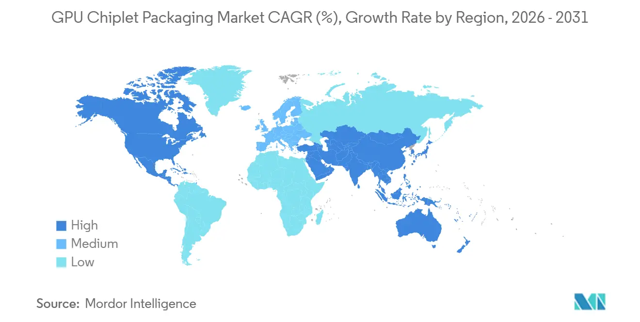
- By geography, Asia-Pacific led with 88.44% share in 2025, while North America is projected to post the fastest CAGR at 23.42% through 2031.
Note: Market size and forecast figures in this report are generated using Mordor Intelligence’s proprietary estimation framework, updated with the latest available data and insights as of January 2026.
Market Trends and Insights
Drivers Impact Analysis of GPU Chiplet Packaging Market*
| Driver | (~) % Impact on CAGR Forecast | Geographic Relevance | Impact Timeline |
|---|---|---|---|
| Rising AI GPU Demand for HBM-Attached Packages | +6.2% | Global | Short term (≤ 2 years) |
| Heterogeneous Integration for Datacenter Performance Scaling | +4.8% | North America and Asia-Pacific core, spill-over to Europe | Medium term (2-4 years) |
| Yield Advantage of Smaller GPU Chiplets Versus Monolithic Dies | +3.5% | Global | Medium term (2-4 years) |
| Advanced Packaging Capacity Investments by Foundries and OSATs | +2.8% | Asia-Pacific core, spill-over to North America | Medium term (2-4 years) |
| Resilient Supply Chain Shift Toward Chiplet-Based Design Reuse | +2.1% | North America, Europe, and Asia-Pacific | Long term (≥ 4 years) |
| GPU Roadmaps Requiring Multi-Die Thermal and Power Optimization | +1.6% | Global | Long term (≥ 4 years) |
| Source: Mordor Intelligence | |||
Rising AI GPU Demand for HBM-Attached Packages
Hyperscaler AI infrastructure spending remains the clearest near-term demand driver for the GPU chiplet packaging market. NVIDIA’s data center segment generated USD 75.2 billion in Q1 FY2027, the quarter ending April 2026, and this was 92% higher than the prior year, while Q2 FY2027 guidance was set at USD 91.0 billion.[1] The draft links that product ramp directly to package complexity, because each Blackwell B200 package combines 2 compute dies with 8 HBM3E stacks on a CoWoS-L substrate. That configuration means each new AI GPU order translates into direct demand for advanced packaging lines, advanced substrates, and high-density memory integration. The result is that the GPU chiplet packaging market is no longer being shaped mainly by broad semiconductor cycles, but by the timing of very large accelerator deployments. This also explains why packaging capacity has become a strategic bottleneck rather than a routine back-end manufacturing step.
Heterogeneous Integration for Datacenter Performance Scaling
Heterogeneous integration has become a core performance lever because simple process shrinks no longer deliver enough system-level gain for leading accelerators. Intel stated that Foveros Direct 3D achieves sub-10 µm interconnect pitch through direct copper-to-copper bonding and can provide up to 10x finer interconnect density than conventional microbump approaches.[2] That level of density supports the vertical die-stacking layouts needed when compute, memory, and I/O functions must operate within a very small physical distance. The same architectural logic is moving beyond flagship GPUs and into custom AI inference silicon programs designed by hyperscaler teams. This broadens the addressable volume base for the GPU chiplet packaging market beyond the standard GPU vendor roadmap. It also raises the importance of packaging teams that can work across design, thermal, and assembly constraints at the same time.
Yield Advantage of Smaller GPU Chiplets Versus Monolithic Dies
Chiplet-based architectures improve yield economics because defect exposure increases as die area rises. The draft describes a clear difference between very large monolithic interposers and smaller local silicon bridge approaches used in CoWoS-L style designs. It notes that local bridge dies can yield near 90%, while equivalently large monolithic interposers can yield near 60%, which materially changes the cost profile of large accelerator packages. Smaller reusable dies also let suppliers adapt one qualified compute element across data center, HPC, and workstation products without repeating the full design effort each time. IEEE’s Heterogeneous Integration Roadmap identifies design reuse and cost recovery across adjacent SKUs as a major business reason for multi-die integration, not just a technical one. This makes the GPU chiplet packaging market more attractive for vendors that want both performance scaling and broader portfolio reuse.
Advanced Packaging Capacity Investments by Foundries and OSATs
Capacity expansion by foundries and OSATs is raising the medium-term ceiling for the GPU chiplet packaging market. ASE Technology Holding broke ground in 2026 on a new Kaohsiung facility with NTD 17.8 billion (USD 548 million), in planned investment to support AI chip advanced packaging and testing.[3] Amkor Technology also broke ground in October 2025 on a USD 7 billion advanced packaging and test campus in Peoria, Arizona, supported by up to USD 400 million in CHIPS Act funding, with TSMC committed under a 10-year procurement agreement. The U.S. Department of Commerce separately confirmed preliminary support terms for Amkor under the CHIPS incentive framework. These projects show that advanced packaging capacity is now being treated as strategic infrastructure by both public agencies and major semiconductor customers. Even with that spending, the GPU chiplet packaging market will remain supply-constrained in the near term because equipment delivery, process tuning, and customer qualification still take time.
Restraints Impact Analysis of GPU Chiplet Packaging Market*
| Restraint | (~) % Impact on CAGR Forecast | Geographic Relevance | Impact Timeline |
|---|---|---|---|
| High Packaging Cost and Limited High-Volume Capacity | -3.8% | Global | Short term (≤ 2 years) |
| Thermal and Signal Integrity Complexity in Dense Interconnects | -2.4% | Global | Medium term (2-4 years) |
| Ecosystem Lock-In Around Proprietary Packaging Platforms | -1.6% | North America and Asia-Pacific | Long term (≥ 4 years) |
| Qualification Risk Across GPU, Memory, and Substrate Suppliers | -1.0% | Global | Medium term (2-4 years) |
| Source: Mordor Intelligence | |||
High Packaging Cost and Limited High-Volume Capacity
High package cost still limits the broad adoption of leading-edge configurations to the highest-value compute programs. The draft states that CoWoS-L packaging for current-generation AI GPUs requires added local silicon bridge elements, higher microbump counts, and lower early-stage assembly yields than simpler CoWoS-S designs. That cost difference matters because the same customers driving market growth are also reserving much of the available qualified capacity. The supply issue is wider than assembly alone, since substrates, specialty materials, and bonding tools all have to scale together for commercial output to increase smoothly. Each new package also needs coordinated qualification across GPU, HBM, and substrate suppliers before revenue can ramp. As a result, the GPU chiplet packaging market faces a structural mismatch between strong demand visibility and slower supply readiness.
Thermal and Signal Integrity Complexity in Dense Interconnects
Thermal and signal integrity issues become harder to manage as chiplet counts rise and HBM stacks get taller. IEEE’s Heterogeneous Integration Roadmap states that differential thermal expansion across silicon, substrates, and molding compounds requires co-design across architecture, circuit, and system levels. A 2025 review in Nanomaterials reported that advanced cooling structures reduced peak GPU temperature from 120°C to 71°C in research configurations. Those approaches improve thermal control, but they also add process complexity that can reduce yield when transferred into high-volume manufacturing. At very fine interconnect pitches, electrical margins also tighten and packaging validation becomes more demanding. This keeps engineering cost and schedule risk elevated across the GPU chiplet packaging market, especially for first-time package designs.
*Our forecasts treat driver/restraint impacts as directional, not additive. The impact forecasts reflect baseline growth, mix effects, and variable interactions.
GPU Chiplet Packaging Market Segment Analysis
By GPU Platform:
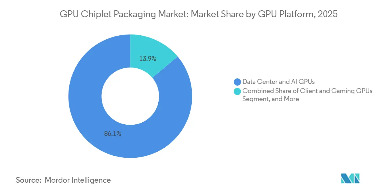
Data Center Demand Redefines Packaging Complexity BenchmarksData Center and AI GPUs held 86.11% of GPU chiplet packaging market share in 2025 and are projected to expand at a 23.21% CAGR through 2031. This concentration reflects the fact that hyperscalers and enterprise AI programs are ordering the most packaging-intensive devices, not the highest historical unit-volume devices. These platforms require CoWoS-L, advanced organic substrate flip-chip, or 3D integration methods that carry far more packaging value per chip than standard client graphics products. NVIDIA’s data center segment revenue of USD 75.2 billion in Q1 FY2027 provides a current-year anchor for the demand intensity behind this category. The GPU chiplet packaging market is therefore being led by the platform class that combines the greatest memory bandwidth needs with the greatest package complexity.
HPC GPUs form the second-largest platform in the draft and serve scientific computing, climate modeling, and defense workloads that still require highly capable 2.5D packaging. Their volumes are lower than the AI accelerator class, but their performance and reliability needs remain demanding. Professional and workstation GPUs sit in a middle tier, where advanced organic substrate solutions are more common than full silicon interposer integration. Client and gaming GPUs still represent a large unit base, but they produce less advanced packaging revenue per chip because their package structures are less dense and less memory intensive. This gap between unit volume and packaging value is widening as AI accelerators move to larger package footprints and higher HBM stack counts. That widening gap reinforces the premium position of data center GPUs within the GPU chiplet packaging market.

By Packaging Technology:
3D Stacked Integration Gains Ground as AI Density Requirements Climb2.5D Interposer and Bridge-Based Packaging accounted for 68.33% of GPU chiplet packaging market size in 2025, while 3D Stacked and Hybrid-Bonded Packaging is forecast to grow at a 23.62% CAGR through 2031. The present leadership of 2.5D formats reflects proven manufacturing readiness across current AI accelerators in commercial shipment. TSMC’s CoWoS family and Intel’s EMIB platform established a production base that current customers already trust for volume delivery and package reliability. Intel also positioned Foveros Direct 3D as a next-stage path for tighter direct bonding and denser vertical integration. This means the GPU chiplet packaging market is still anchored by 2.5D revenue even as 3D technologies gain strategic importance.
The draft shows that 3D stacked and hybrid-bonded formats are gaining momentum because future memory and logic designs need much finer interconnect geometry than conventional microbump flows can support. Fan-Out and RDL-based packaging provides an alternative path for customers that need advanced integration without the full cost profile of silicon interposer approaches. Organic substrate-based multi-die packaging remains relevant for client GPU and entry workstation programs where bandwidth density and thermal load are more moderate. Standards compliance is also becoming more important because high-bandwidth memory interfaces and die-to-die connections have to qualify within tighter electrical and thermal limits. This puts process maturity, not just novelty, at the center of commercial adoption. As a result, the GPU chiplet packaging market is likely to move in stages, with 2.5D staying dominant in volume while 3D expands first in the highest-value programs.
By Chiplet Function:
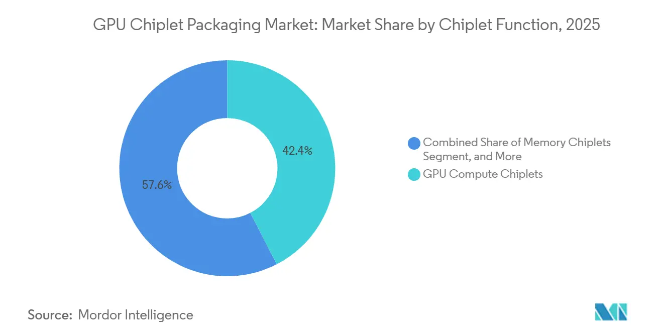
HBM Integration Emerges as the Decisive Growth VariableGPU Compute Chiplets represented 42.42% of the market by chiplet function in 2025, while Memory Chiplets and HBM Integration is projected to grow at a 23.53% CAGR through 2031. Compute chiplets remain the highest-value dies in major accelerator packages because they define the architecture, the power profile, and much of the thermal envelope. They also determine how the rest of the package has to be laid out, including bridge placement, substrate routing, and memory proximity. The faster expansion of memory chiplets and HBM integration shows how much package design is now being shaped by bandwidth demand rather than compute density alone. The GPU chiplet packaging market is increasingly influenced by how many memory stacks each new platform generation carries and how closely those stacks must sit to the compute dies.
The shift from HBM3E to HBM4 raises the importance of memory-side packaging because stack height, interconnect density, and package-level yield all become harder to manage together. I/O and base die chiplets serve as the routing and power layer that keeps larger packages electrically and thermally stable as footprints grow. Connectivity and interface chiplets are also becoming more important as the draft points toward co-packaged optics and denser system integration paths. This makes package architecture less linear, because compute, memory, interface, and power functions all have to be balanced inside the same assembly plan. In that setting, memory integration becomes one of the strongest variables shaping cost, yield, and product timing. That is why the GPU chiplet packaging industry is seeing HBM integration move from a supporting role to a central growth driver.
By Application:
AI Workloads Establish a Structural Demand Floor Across All SegmentsAI Training and Inference accounted for 69.12% of the market by application in 2025 and is projected to record a 23.32% CAGR through 2031. This leadership reflects the fact that the most advanced GPU packages are being deployed first where very large models need both dense memory bandwidth and sustained throughput. Every large AI training cluster and every hyperscaler-scale inference rollout reinforces demand for HBM-attached chiplet accelerators with sophisticated package structures. The draft also distinguishes between training and inference behavior, noting that inference often scales through larger installed bases rather than through only the highest compute density per device. That dynamic broadens the shipment base for the GPU chiplet packaging market even within the same application family.
High-performance computing remains the second-largest application, supported by government, research, and scientific workloads that continue to demand advanced 2.5D integration and strong thermal reliability. Cloud computing works as both an application layer and a deployment model because the same packaged GPU platforms can support AI, simulation, and general-purpose acceleration. Professional visualization stays relevant through engineering, simulation, and content creation use cases that need steady but less extreme package performance. Gaming and consumer graphics remain the largest historical unit-volume application, but they generate lower advanced packaging revenue per chip than AI or HPC. That revenue gap is widening because AI accelerators keep adding packaging content while gaming products remain in simpler structures. The GPU chiplet packaging market is therefore becoming more dependent on application value intensity than on unit shipment counts alone.
By End User:
Hyperscalers Define the Supply Chain and Custom Silicon Reshapes the Competitive MapHyperscalers and Cloud Providers held 61.65% of the market by end user in 2025 and are projected to expand at a 23.28% CAGR through 2031. This customer group shapes procurement timing, package qualification priorities, and the allocation of the most advanced back-end capacity. The draft makes clear that suppliers without a direct hyperscaler relationship face a weaker position when trying to secure leading-edge CoWoS or SoIC access. It also notes that custom silicon programs from major cloud platforms are expanding the set of chips competing for the same advanced package resources. This means the GPU chiplet packaging market is being influenced not only by merchant GPU vendors, but also by captive accelerator teams inside the largest cloud companies.
Enterprise data centers form the second-largest end-user segment and are gradually moving toward owned AI infrastructure as workloads mature and utilization improves. Research and government HPC centers remain smaller in absolute share, but they are strategically important because they continue to demand frontier packaging performance for national computing programs. OEMs and system integrators act as distribution multipliers by embedding packaged accelerators into servers, workstations, and specialized compute systems. The draft also points to long lead times for advanced packaged GPU systems, which encourages earlier purchasing commitments from many enterprise buyers. That behavior improves demand visibility for established suppliers while making late entry harder for new ones. In that sense, the GPU chiplet packaging industry is being shaped as much by customer structure and procurement behavior as by technology alone.
Geography Analysis
APAC GPU Chiplet Packaging Market
Asia-Pacific held 88.44% of the GPU chiplet packaging market share in 2025, which reflects the region’s deep concentration of foundries, OSATs, substrate suppliers, and memory producers. Taiwan anchors this ecosystem through TSMC’s advanced packaging base and ASE Technology Holding’s scale in outsourced semiconductor assembly and test. Taiwan’s advantage is not only production capacity, but also supply chain proximity across packaging materials, substrates, and engineering talent. South Korea supports the regional position through HBM memory leadership and related package integration capabilities that remain critical for AI accelerators. Japan also retains strategic relevance because ABF substrate production from local suppliers sits at a key chokepoint in the wider packaging chain.
North America GPU Chiplet Packaging Market
North America is forecast to grow at a 23.42% CAGR through 2031, making it the fastest-growing regional cluster in the GPU chiplet packaging market. The CHIPS and Science Act created a stronger investment base for domestic manufacturing and packaging, with public and private incentives totaling USD 46.7 billion in the cited CRS report. Amkor’s Arizona advanced packaging campus and GlobalFoundries’ New York Advanced Packaging and Photonics Center are the clearest operating examples of that policy-backed buildout. GlobalFoundries said its New York center opened in January 2025 with USD 575 million in investment and USD 75 million in direct CHIPS Act support. The region’s growth rate is strong because it is starting from a low base, not because it is close to displacing Asia-Pacific in current installed capacity.
EMEA and South America GPU Chiplet Packaging Market
Europe holds a modest commercial position in the GPU chiplet packaging market, but it remains important in 3D integration and heterogeneous packaging research. The region’s relevance comes more from technology development at centers such as imec, Fraunhofer institutes, and CEA-Leti than from large qualified production volumes. South America, the Middle East, and Africa remain early-stage demand regions and do not yet have material leading-edge packaging manufacturing bases. The Middle East is emerging as a demand node through sovereign AI investment programs, while Africa’s role remains tied to broader data center buildout and imported accelerator supply.
Competitive Landscape
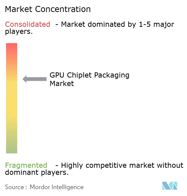
The GPU chiplet packaging market remains highly concentrated at the leading edge, with TSMC holding the strongest position in CoWoS-L for current AI GPU programs. That position gives TSMC significant influence over product timing, customer prioritization, and packaging migration paths because many leading accelerators depend on its qualified process stack. ASE Technology Holding remains a major OSAT competitor and is expanding AI-focused capacity through its Kaohsiung facility investment announced in 2026. Intel is the clearest direct technology challenger through EMIB and Foveros Direct 3D, which target dense multi-die and hybrid-bonded integration needs. The competitive structure therefore centers on a narrow supplier group that can meet the required pitch, yield, and reliability standards for the most advanced AI packages.
Partnerships and long-term commitments are becoming as important as pure process capability in the GPU chiplet packaging market. NVIDIA and Intel announced a co-development agreement in September 2025, backed by a USD 5 billion NVIDIA investment, and both companies identified Intel’s packaging platform as the core technology rationale. Amkor’s Arizona campus also moved forward with TSMC committed under a 10-year procurement agreement, while Apple and NVIDIA were named as anchor customers. These moves show that strategic alignment across foundries, OSATs, and system vendors now plays a direct role in who can scale fastest.
White-space opportunities are forming around panel-level packaging, glass interposers, and co-packaged optics, even though the mainstream market is still led by established 2.5D flows. Suppliers that can lower cost without losing interconnect density could gain traction in mid-tier AI and custom silicon programs that do not need the very highest package complexity. Chinese and broader Asian OSAT players are adding capacity and trying to move into higher-value programs, but qualification depth still separates them from the top tier. For the near term, the GPU chiplet packaging market is likely to stay concentrated because only a limited number of companies can support the most advanced package types at commercial scale.
GPU Chiplet Packaging Industry Leaders
-
NVIDIA Corporation
-
Taiwan Semiconductor Manufacturing Company Limited
-
Advanced Micro Devices, Inc.
-
Samsung Electronics Co., Ltd.
-
Intel Corporation
- *Disclaimer: Major Players sorted in no particular order
GPU Chiplet Packaging Market Companies Covered in this Report
- NVIDIA Corporation
- Advanced Micro Devices, Inc.
- Taiwan Semiconductor Manufacturing Company Limited
- Intel Corporation
- Samsung Electronics Co., Ltd.
- SK hynix Inc.
- Micron Technology, Inc.
- Amkor Technology, Inc.
- ASE Technology Holding Co., Ltd.
- JCET Group Co., Ltd.
- Tongfu Microelectronics Co., Ltd.
- SPIL, Siliconware Precision Industries Co., Ltd.
- Powertech Technology Inc.
- Unimicron Technology Corporation
- Shinko Electric Industries Co., Ltd.
- Murata Manufacturing Co., Ltd.
- Ibiden Co., Ltd.
- Kyocera Corporation
- ASE Group
- TSMC
- GlobalFoundries Inc.
Recent Industry Developments in GPU Chiplet Packaging Market
- March 2026: ASE Technology Holding broke ground on a new high-tech facility in Kaohsiung, Taiwan, requiring NTD 17.8 billion (USD 548 million) in investment. The facility targets AI chip advanced packaging and testing, integrating logistics, manufacturing, and testing within a single smart-factory campus.
- January 2026: Tongfu Microelectronics announced plans to raise RMB 4.4 billion (USD 611 million) through private placement to expand packaging and testing capacity across memory chips, wafer-level packaging, and computing communications applications, with the stated goal of reinforcing its position as the fourth-largest global OSAT.
- January 2026: GlobalFoundries completed one year of announcement for the New York Advanced Packaging and Photonics Center within its Malta, New York facility, with a USD 575 million total investment supplemented by USD 75 million in direct CHIPS Act funding and USD 550 million from New York State’s Green CHIPS program. The center offers wafer-to-wafer bonding, 3D heterogeneous integration, and silicon photonics turnkey packaging, creating approximately 100 new jobs over 5 years.
- October 2025: Amkor Technology broke ground on a USD 7 billion advanced packaging and test campus in Peoria, Arizona, the first high-volume domestic OSAT facility in the United States, backed by up to USD 400 million in CHIPS Act direct funding from the U.S. Department of Commerce. TSMC committed to a 10-year procurement agreement and Apple and NVIDIA were named as anchor customers.
Global GPU Chiplet Packaging Market Report Scope
The Global GPU Chiplet Packaging Market refers to the industry segment focused on the design and deployment of advanced semiconductor packaging technologies that utilize chiplet architectures to build high-performance Graphics Processing Units (GPUs).
The GPU Chiplet Packaging Market Report is Segmented by GPU Platform (Data Center and AI GPUs, HPC GPUs, Professional and Workstation GPUs, Client and Gaming GPUs, and Other GPU Platforms), Packaging Technology (2.5D Interposer and Bridge-Based Packaging, 3D Stacked and Hybrid-Bonded Packaging, Fan-Out and RDL-Based Packaging, Organic Substrate-Based Multi-Die Packaging, and Other Packaging Technologies), Chiplet Function (GPU Compute Chiplets, Memory Chiplets, I/O and Base Die Chiplets, Connectivity and Interface Chiplets, and Other Chiplets), Application (AI Training and Inference, High-Performance Computing, Cloud Computing, Professional Visualization, Gaming and Consumer Graphics, and Other Applications), End User (Hyperscalers and Cloud Providers, Enterprise Data Centers, Research and Government HPC Centers, OEMs and System Integrators, and Other End Users), and Geography (North America, Europe, Asia-Pacific, South America, Middle East, and Africa). The Market Forecasts are Provided in Terms of Value (USD).
Segmentation Overview
| Data Center and AI GPUs |
| HPC GPUs |
| Professional and Workstation GPUs |
| Client and Gaming GPUs |
| Other GPU Platforms |
| 2.5D Interposer and Bridge-Based Packaging |
| 3D Stacked and Hybrid-Bonded Packaging |
| Fan-Out and RDL-Based Packaging |
| Organic Substrate-Based Multi-Die Packaging |
| Other Packaging Technologies |
| GPU Compute Chiplets |
| Memory Chiplets |
| I/O and Base Die Chiplets |
| Connectivity and Interface Chiplets |
| Other Chiplets |
| AI Training and Inference |
| High-Performance Computing |
| Cloud Computing |
| Professional Visualization |
| Gaming and Consumer Graphics |
| Other Applications |
| Hyperscalers and Cloud Providers |
| Enterprise Data Centers |
| Research and Government HPC Centers |
| OEMs and System Integrators |
| Other End Users |
| North America | United States |
| Canada | |
| Mexico | |
| Europe | Germany |
| United Kingdom | |
| France | |
| Italy | |
| Rest of Europe | |
| Asia-Pacific | China |
| Japan | |
| South Korea | |
| India | |
| Southeast Asia | |
| Rest of Asia-Pacific | |
| South America | |
| Middle East | |
| Africa |
| By GPU Platform | Data Center and AI GPUs | |
| HPC GPUs | ||
| Professional and Workstation GPUs | ||
| Client and Gaming GPUs | ||
| Other GPU Platforms | ||
| By Packaging Technology | 2.5D Interposer and Bridge-Based Packaging | |
| 3D Stacked and Hybrid-Bonded Packaging | ||
| Fan-Out and RDL-Based Packaging | ||
| Organic Substrate-Based Multi-Die Packaging | ||
| Other Packaging Technologies | ||
| By Chiplet Function | GPU Compute Chiplets | |
| Memory Chiplets | ||
| I/O and Base Die Chiplets | ||
| Connectivity and Interface Chiplets | ||
| Other Chiplets | ||
| By Application | AI Training and Inference | |
| High-Performance Computing | ||
| Cloud Computing | ||
| Professional Visualization | ||
| Gaming and Consumer Graphics | ||
| Other Applications | ||
| By End User | Hyperscalers and Cloud Providers | |
| Enterprise Data Centers | ||
| Research and Government HPC Centers | ||
| OEMs and System Integrators | ||
| Other End Users | ||
| By Geography | North America | United States |
| Canada | ||
| Mexico | ||
| Europe | Germany | |
| United Kingdom | ||
| France | ||
| Italy | ||
| Rest of Europe | ||
| Asia-Pacific | China | |
| Japan | ||
| South Korea | ||
| India | ||
| Southeast Asia | ||
| Rest of Asia-Pacific | ||
| South America | ||
| Middle East | ||
| Africa | ||
Key Questions Answered in the Report
What is the GPU chiplet packaging market size in 2026, and where is it headed by 2031?
The GPU chiplet packaging market stands at USD 11.20 billion in 2026 and is projected to reach USD 29.89 billion by 2031 at a 21.69% CAGR.
Why is demand rising so quickly for advanced GPU packaging?
Demand is rising because AI training and inference accelerators need HBM-attached multi-die package designs, and those designs depend on advanced 2.5D and 3D integration.
Which GPU platform generates the most packaging revenue?
Data Center and AI GPUs lead by a wide margin, with 86.11% share in 2025, because they use the most packaging-intensive configurations.
Which packaging technology leads today and which one is growing fastest?
2.5D Interposer and Bridge-Based Packaging led with 68.33% share in 2025, while 3D Stacked and Hybrid-Bonded Packaging is growing fastest at a 23.62% CAGR through 2031.
Why is Asia-Pacific so dominant in this space?
Asia-Pacific held 88.44% share in 2025 because Taiwan, South Korea, Japan, and China together provide the strongest mix of foundry, OSAT, memory, and substrate capabilities.
What is the main challenge holding the sector back?
The biggest challenge is the combination of high package cost, limited qualified capacity, and the thermal and signal integrity complexity that comes with denser chiplet and HBM designs.