GPU Substrate Market Size and Share
Market Overview
| Study Period | 2020 - 2031 |
|---|---|
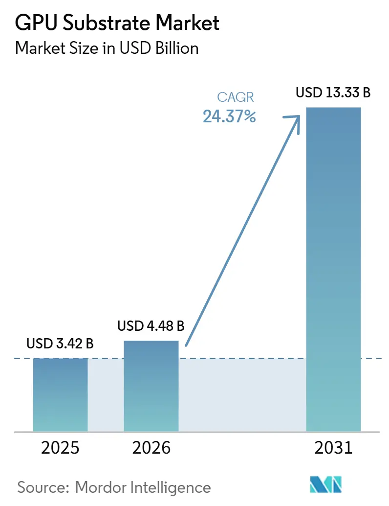
| Market Size (2026) | USD 4.48 Billion |
| Market Size (2031) | USD 13.33 Billion |
| Growth Rate (2026 - 2031) | 24.37% CAGR |
| Fastest Growing Market | Asia-Pacific |
| Largest Market | North America |
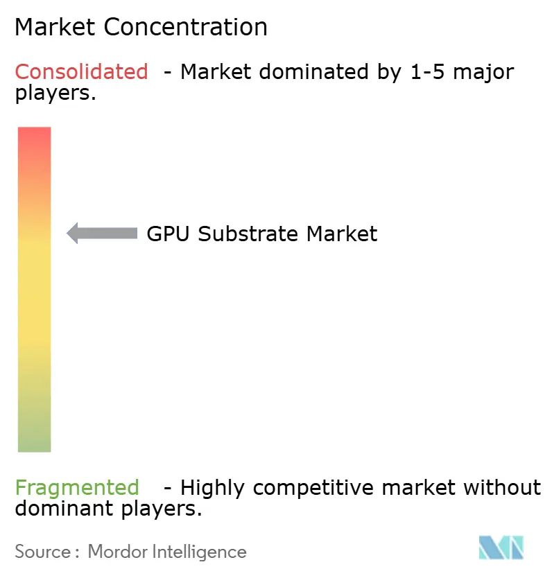
| Market Concentration | Medium |
Major Players *Disclaimer: Major Players sorted in no particular order Image © Mordor Intelligence. Reuse requires attribution under CC BY 4.0. | |
GPU Substrate Market Analysis by Mordor Intelligence
The GPU substrate market size is expected to increase from USD 3.42 billion in 2025 to USD 4.48 billion in 2026 and reach USD 13.33 billion by 2031, growing at a CAGR of 24.37% over 2026-2031. Growth is being driven by sustained AI accelerator deployment, larger package footprints, and the wider use of 2.5D and 3D integration in advanced compute systems. Demand conditions in this market are being shaped more by hyperscale AI infrastructure programs than by consumer electronics replacement cycles, which gives suppliers better forward visibility than in earlier packaging cycles. The GPU substrate market also remains highly sensitive to process yield, because larger and more complex packages raise the technical burden on substrate makers at every additional layer count. Supply remains concentrated among a narrow group of Japanese and Taiwanese specialists, which keeps engineering capability and customer qualification as the main competitive filters. New investment programs in the United States, Europe, and Asia are expanding the long-term capacity base, but the near-term market remains tight because plant ramp-up and customer approval cycles take time.
Key Report Takeaways
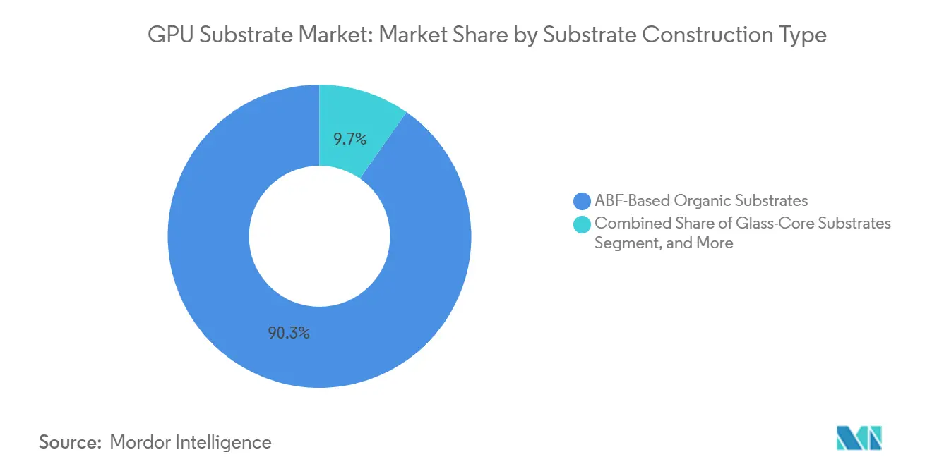
- By substrate construction type, ABF-based organic substrates held 90.28% share of the GPU Substrate Market in 2025, while glass-core substrates are projected to expand at a 24.99% CAGR through 2031.
- By package architecture, 2.5D interposer-based package substrates held 49.79% share of the GPU Substrate Market in 2025, while 3D die-stacked package substrates are projected to expand at a 25.14% CAGR through 2031.
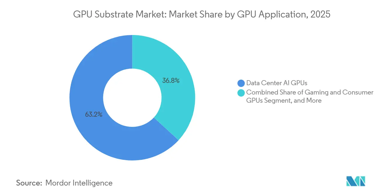
- By GPU application, data center AI GPUs held 63.17% share in 2025, and this segment is projected to expand at a 24.72% CAGR through 2031.
- By end-use industry, hyperscale cloud and AI infrastructure held 58.67% share in 2025 and is projected to expand at a 25.16% CAGR through 2031.
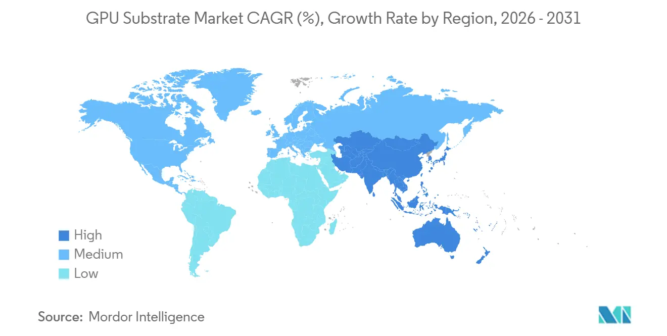
- By geography, North America held 48.44% share in 2025, while the Asia-Pacific is projected to expand at a 25.33% CAGR through 2031.
Note: Market size and forecast figures in this report are generated using Mordor Intelligence’s proprietary estimation framework, updated with the latest available data and insights as of January 2026.
Global GPU Substrate Market Trends and Insights
Drivers Impact Analysis*
| Driver | (~) % Impact on CAGR Forecast | Geographic Relevance | Impact Timeline |
|---|---|---|---|
| Rising AI GPU Shipments and High-Density Packaging Demand | +4.5% | Global, highest intensity in North America and Asia-Pacific | Short term (≤ 2 years) |
| Shift to Chiplet-Based GPU Architectures | +3.5% | Global, led by Taiwan, Japan, and United States | Medium term (2-4 years) |
| Expansion of Hyperscale Data Centers and AI Clusters | +3.0% | North America dominant, spillover to Middle East and Africa and Asia-Pacific | Short term (≤ 2 years) |
| Supply Localization Incentives for Advanced Packaging Capacity | +1.5% | North America and Europe core, early gains in India and Southeast Asia | Long term (≥ 4 years) |
| Increasing Build-Up Layer Counts and Interconnect Density Requirements | +1.0% | Global, centered on Japan and Taiwan supply base | Medium term (2-4 years) |
| Adoption of Advanced Thermal Management Substrate Designs | +0.5% | Global, with strong R&D activity in Japan, the United States, and South Korea | Long term (≥ 4 years) |
| Source: Mordor Intelligence | |||
Rising AI GPU Shipments And High-Density Packaging Demand
The GPU substrate market is growing faster than shipment counts alone would suggest, because current AI accelerators use much larger packages and much heavier build-up requirements than earlier GPU platforms. In the GPU substrate market, this change lifts substrate area consumption per finished device as memory integration, power delivery, and signal routing all become more demanding within the same package envelope. The commercial effect is already visible in supplier strategy, since leading companies are directing expansion toward high-performance IC package substrates tied to AI server programs rather than broad exposure to lower-value printed circuit categories. Ibiden said in February 2026 that its electronics investment plan is focused on high-performance IC package substrates, with mass production at new plants expected from fiscal 2027. Samsung Electro-Mechanics also said its high-value FC-BGA portfolio for servers, AI, automotive, and network applications is set to account for more than 50% of its substrate revenue by 2026.[1]Samsung Electro-Mechanics, “Samsung Electro-Mechanics' FCBGA Recognized by Global Customers, Target to Increase High-Value FCBGA to 50% by 2026,” samsungsem.com As a result, the GPU substrate market is being shaped by platforms that demand high yield at advanced specifications, which gives experienced suppliers a stronger position in pricing, allocation, and customer qualification.
Shift To Chiplet-Based GPU Architectures
The GPU substrate market is also being lifted by the move toward chiplet-based designs, because multi-die layouts place logic, memory, and I/O elements on the same package and raise both substrate complexity and usable area. In the GPU substrate market, this matters because advanced package formats must support finer routing, tighter warpage control, and more demanding thermal behavior than monolithic layouts. A peer-reviewed paper presented at IEEE ECTC 2025 showed that advanced 2.5D liquid-cooled packages with embedded thermal structures can handle thermal design powers above 400 watts while keeping die temperatures within acceptable limits, which reflects the engineering load created by denser multi-die assemblies.[2]IEEE, “First Demonstration of Metal-Lidded Integral Microjet Impingement On-Chip Cooling Structures With Alternating Feeding and Draining Nozzles for High-Performance Interposer Packages,” doi.org That evidence helps explain why the GPU substrate market is placing greater value on process control, flatness, and yield consistency as package complexity rises. It also clarifies why glass-core development, hybrid bonding readiness, and ultra-flat large-panel processing are receiving more attention across advanced packaging ecosystems. The result is that the GPU substrate market is moving toward a technology ladder where each new architecture raises qualification difficulty for suppliers that are not already embedded in advanced GPU programs.
Expansion Of Hyperscale Data Centers And AI Clusters
Hyperscale data center expansion remains the central demand anchor for the GPU substrate market, because large cloud operators are locking in accelerated computing capacity well ahead of deployment schedules. In the GPU substrate market, this demand is more predictable than in earlier packaging cycles, since procurement for AI systems is increasingly tied to multi-quarter infrastructure programs rather than short replacement patterns. NIST's January 2025 awards under the National Advanced Packaging Manufacturing Program showed that the United States is treating advanced substrate and materials capability as a strategic part of future compute infrastructure.[3]National Institute of Standards and Technology, “National Advanced Packaging Manufacturing Program,” nist.gov The same policy direction appears in the U.S. Department of Commerce support framework for advanced packaging projects, which is intended to build domestic capacity in critical semiconductor packaging steps. These moves matter because the GPU substrate market sits close to the center of AI server buildouts, and any increase in advanced package deployment raises demand for high-specification substrate panels. That keeps supplier planning tied closely to the spending cadence of a small number of large customers, which strengthens visibility for qualified producers but also increases exposure to concentrated buyer decisions.
Supply Localization Incentives For Advanced Packaging Capacity
Supply localization incentives are reshaping the GPU substrate market by pushing capacity and R&D activity closer to the end customers that design or deploy advanced AI systems. In the GPU substrate market, this does not remove Asia's leadership, but it does create new qualification routes for suppliers that can meet regulatory, technical, and security requirements. NIST awarded support to Absolics under the National Advanced Packaging Manufacturing Program, reinforcing the U.S. push to develop advanced substrate manufacturing capability and materials depth. The same program also finalized USD 300 million of awards to Absolics, Applied Materials, and Arizona State University for advanced substrate and substrate materials R&D in January 2025. Ibiden also said it started construction of a new flip-chip package substrate plant in Phoenix, Arizona, under CHIPS Act support, which shows how localization is moving from policy language to physical capacity. Over time, that will broaden the geographic footprint of the GPU substrate market, even though most proven high-volume capability still remains in Japan and Taiwan today.
Restraints Impact Analysis*
| Restraint | (~) % Impact on CAGR Forecast | Geographic Relevance | Impact Timeline |
|---|---|---|---|
| High Capital Intensity and Long Ramp-Up Cycles | -1.5% | Global, most acute in North America and Europe where base capacity is thin | Long term (≥ 4 years) |
| Yield Losses at Very High Layer Counts | -1.0% | Global, concentrated impact at Japan and Taiwan lead manufacturers | Medium term (2-4 years) |
| Concentrated ABF Material Supply Base | -0.7% | Global upstream, material bottleneck originates in Japan | Short term (≤ 2 years) |
| Emerging Glass and RDL-First Alternatives | -0.3% | Global R&D, with commercialization centered in the United States, Japan, and South Korea | Long term (≥ 4 years) |
| Source: Mordor Intelligence | |||
High Capital Intensity And Long Ramp-Up Cycles
The GPU substrate market faces a clear constraint in the form of high capital intensity, because advanced facilities require large upfront investment and long qualification periods before revenue can scale. In the GPU substrate market, that makes customer-backed expansion more common than independent capacity bets, especially for the highest layer counts and the most demanding package formats. Ibiden approved an investment plan of JPY 500 billion, or USD 3.33 billion, for fiscal 2026 to 2028, with new mass production expected from fiscal 2027. AT&S said in June 2026 that expanding high-end IC substrate capacity at Kulim required EUR 1.5 billion to EUR 2.0 billion, or USD 1.68 billion to USD 2.24 billion, fully financed by long-term customer commitments. Those commitments show that supply growth in the GPU substrate market is often gated by the willingness of a narrow customer group to underwrite capacity before output is available. That lag keeps the market tight even when investment announcements are large, because building, qualifying, and ramping a new plant takes longer than current demand growth.
Yield Losses At Very High Layer Counts
Yield losses at very high layer counts remain a serious operational brake on the GPU substrate market, because every added layer increases process steps, warpage risk, and the probability of defects that reduce usable output. In the GPU substrate market, this issue becomes more severe as package sizes expand and routing density rises for AI accelerators that combine logic, memory, and advanced cooling requirements. The IEEE ECTC 2025 work on liquid-cooled interposer packages shows that thermal and structural demands are moving upward alongside compute density, which raises the difficulty of manufacturing reliable high-performance package platforms. That is why suppliers with proven high-layer-count yield capability continue to command premium positions in the GPU substrate market, even when other manufacturers announce new capital programs. The qualification cycle also slows competitive catch-up, because customers typically need sustained evidence of process stability before approving a new substrate source for advanced GPU programs. As a result, nominal capacity additions do not translate into effective supply at the same pace, and the yield gap remains a practical barrier to faster market balancing.
*Our forecasts treat driver/restraint impacts as directional, not additive. The impact forecasts reflect baseline growth, mix effects, and variable interactions.
Segment Analysis
By Substrate Construction Type: ABF Lock-In Persists As Glass-Core Substrates Move Closer To Qualification
ABF-based organic substrates held 90.28% of the GPU substrate market share in 2025, while glass-core substrates are projected to expand at a 24.99% CAGR through 2031. That spread shows how firmly ABF remains embedded in current GPU and AI accelerator packaging, especially where high-layer counts, signal integrity, and production yield matter more than experimentation with new materials. The draft also makes clear that this leadership is not just a matter of installed base, because the supply chain around ABF is already aligned to the strict performance requirements of present advanced compute programs. BT and epoxy-based organic substrates continue to serve lower-layer-count GPU uses, mainly in gaming and professional visualization, where cost and established process flows remain important. Coreless organic substrates are drawing interest for thinner edge AI designs, but the draft indicates that mechanical fragility at larger panel sizes still limits broad use in data center-class products.
The GPU substrate industry still revolves around ABF because no alternative in the draft matches current AI program requirements at the same combination of layer count, yield, and commercial readiness. NIST support for Absolics shows that glass substrate development is moving from research to an industrial buildout path in the United States. Samsung Electro-Mechanics also disclosed that high-value FC-BGA linked to servers, AI, automotive, and network applications is becoming a larger share of its portfolio, which reinforces the push toward higher-performance substrate formats. Within the GPU substrate market, that means glass-core progress matters less as an immediate volume threat and more as a qualification path that could influence the top end of future package roadmaps. The overall mix, therefore, remains stable in the near term, with ABF carrying present revenue and glass-core shaping where the GPU substrate industry may compete next.


By Package Architecture: Interposer Scale Holds Volume While 3D Stacking Gains Strength
The 2.5D interposer-based package substrates segment accounted for 49.79% of the GPU substrate market size in 2025, while 3D die-stacked package substrates are projected to expand at a 25.14% CAGR through 2031. This lead reflects the commercial maturity of 2.5D packaging and its compatibility with high bandwidth memory integration, which has made it the default path for many current AI GPU designs. FC-BGA remains the second-largest architecture by value, because it supports mainstream data center and gaming GPU requirements without the full cost structure of a silicon interposer. FC-CSP continues to address compact edge AI and workstation products, where board space and package thickness influence design decisions more directly than extreme performance targets. Fan-out and RDL-based formats are also present in the draft, but their role remains more relevant for thin and compact products than for the largest data center packages.
The GPU substrate market is now balancing the proven volume role of 2.5D against the longer-term promise of 3D logic and memory stacking, and that balance is defining current packaging roadmaps. A peer-reviewed IEEE ECTC 2025 paper showed that advanced 2.5D packages with embedded cooling structures can manage thermal design powers above 400 watts, which helps explain why 2.5D still has room to scale before a full architectural shift is required. That finding matters because thermal performance and package flatness are now moving alongside electrical requirements as key success factors for the GPU substrate market. The draft also shows that 3D die-stacked formats are gaining momentum as logic-under-memory concepts and hybrid bonding move closer to wider commercialization. For suppliers, the main implication is that architectural growth is no longer just a matter of routing density, because cooling, warpage control, and large-format process stability now shape competitiveness across the GPU substrate market.
By GPU Application: Data Center AI Sets The Pace For Revenue And Technical Complexity
Data center AI GPUs accounted for 63.17% of the GPU substrate market in 2025, making this the clearest application center for substrate revenue and technical development. That dominance is rooted in the fact that each new AI accelerator generation uses larger and more complex packages, so substrate revenue rises faster than shipment counts alone would suggest. HPC and scientific computing GPUs remain the second-largest application group in the draft, supported by supercomputing programs and compute-heavy research workloads that need sustained performance. Gaming and consumer GPUs still contribute important shipment volume, but their share has compressed as AI server deployments have expanded much faster. Professional visualization and workstation products provide a steadier demand base, with less volatility than gaming and less scale than hyperscale AI systems.
The GPU substrate market also has smaller but relevant growth channels in edge AI, embedded inference, and automotive compute, each with distinct package and reliability needs. Edge AI favors miniaturized and power-efficient substrate formats, which is why fan-out and coreless concepts appear more often in that part of the mix than in data center systems. Automotive GPU programs remain a long-cycle opportunity in the GPU substrate market, because thermal and mechanical qualification requirements extend well beyond those in consumer devices. This mix shows that the center of gravity has shifted decisively toward AI infrastructure, even though legacy GPU categories continue to support volume, process learning, and secondary demand streams. The application structure therefore reinforces the view that future gains in the GPU substrate market will be determined more by advanced compute deployment than by traditional graphics cycles.
By End-Use Industry: Hyperscale Cloud Anchors Demand While Adjacent Uses Broaden The Base
Hyperscale cloud and AI infrastructure accounted for 58.67% of the GPU substrate market size in 2025 and is projected to expand at a 25.16% CAGR through 2031. This position makes hyperscalers the strongest demand shapers in the GPU substrate market, because their procurement plans influence capacity timing, qualification priorities, and revenue visibility for suppliers. Enterprise and colocation data centers form the next demand layer, driven by private AI clusters and on-premises inference systems that follow hyperscaler adoption with a time lag. HPC, government, and defense spending adds stability to the mix, because sovereign AI and supercomputing programs are less exposed to short commercial budget cycles. Consumer electronics and gaming now represent a smaller share of end-use demand than they did in earlier packaging cycles, since their substrate requirements are less intense than those in AI servers.
The GPU substrate market is also building a longer runway in automotive, industrial, telecom, and edge computing uses, although those segments move at a slower qualification pace. Automotive programs typically require extended approval cycles, which means design wins secured in 2025 and 2026 are more likely to translate into revenue later in the forecast period than immediately. Industrial and telecom demand remains fragmented, but it expands the addressable base for substrate formats optimized around power efficiency and compact system integration. Within the GPU substrate industry, this end-use mix matters because the largest buyers set the performance standard that smaller segments eventually follow. The overall pattern is that the GPU substrate market remains anchored by hyperscale AI demand today, while several adjacent uses widen the future revenue base without yet challenging that core.
Geography Analysis
North America held 48.44% of the GPU substrate market share in 2025, and that lead reflected its concentration of GPU designers and hyperscaler customers. The region's position was driven by demand ownership rather than manufacturing scale, since many leading substrate panels are still produced in Asia and shipped into U.S.-centered design and server ecosystems. The GPU substrate market in North America is also being supported by localization programs that are expanding advanced packaging and substrate capability closer to end customers. NIST finalized USD 300 million in January 2025 awards for advanced substrate and substrate materials R&D, which helped lay institutional groundwork for domestic development. Ibiden's Arizona investment and the U.S. Department of Commerce support framework for Amkor show that North America is trying to reduce structural dependence on overseas advanced packaging capacity.
Asia-Pacific is projected to expand at a 25.33% CAGR through 2031, making it the fastest-growing regional block in the GPU substrate market. Japan remains the deepest production base in the draft, because it combines major substrate manufacturers with the upstream ABF material ecosystem that supports leading GPU programs. Taiwan continues to hold a central role through suppliers that serve advanced FC-BGA and AI package demand, and that entrenched manufacturing position keeps the region critical to near-term supply continuity. South Korea is also moving into more advanced substrate categories, with Samsung Electro-Mechanics positioning high-value substrate applications as a larger share of its portfolio. The region contains the broadest mix of incumbent scale, challenger investment, and materials know-how, which is why the GPU substrate market still depends on Asia-Pacific for most proven high-volume capability.
Europe held a smaller but strategically meaningful position in the GPU substrate market in 2025, with AT&S acting as the region's most visible advanced substrate player. AT&S said in June 2026 that its Kulim facility expansion for high-end IC substrates required EUR 1.5 billion to EUR 2.0 billion, or USD 1.68 billion to USD 2.24 billion, backed by long-term customer commitments. South America and the Middle East and Africa still have minimal substrate manufacturing capacity, even though AI infrastructure demand is beginning to rise in parts of those regions. That means the GPU substrate market remains globally sold but regionally concentrated on the supply side, with Europe adding technology depth and new investment, while most production capability still sits in Asia and demand leadership remains strongest in North America.

Competitive Landscape
The GPU substrate market is concentrated around a small group of suppliers that combine process yield, capital depth, and long-standing engineering ties with leading GPU developers. Ibiden, Shinko Electric Industries, Unimicron, Nan Ya PCB, and AT&S form the core incumbent tier described in the draft, and they remain best positioned for the most demanding AI GPU programs. The GPU substrate market also includes a challenger layer made up of Samsung Electro-Mechanics, LG Innotek, Kinsus, Shennan Circuits, TOPPAN, and emerging glass-core specialists. What separates the top tier is not simple scale alone, but the ability to deliver high-layer-count substrates with consistent yield, stable flatness, and dependable qualification performance at volume. That structure makes competition in the GPU substrate market more dependent on technical execution and customer trust than on short-term price moves.
Ibiden's February 2026 capital plan for JPY 500 billion, or USD 3.33 billion, shows how leading players are expanding specifically around high-performance IC package substrates for AI server programs. AT&S made a similar strategic move in June 2026 when it tied its Kulim high-end IC substrate expansion to long-term customer commitments from AMD and another major technology company. Samsung Electro-Mechanics has also signaled a deliberate push toward higher-value substrate categories, stating that servers, AI, automotive, and network applications are expected to exceed 50% of substrate revenue by 2026. These moves show that the GPU substrate market rewards companies that align capital spending with specific advanced compute programs instead of broad volume chasing. They also show why capacity additions are often announced together with customer agreements, because qualification without committed demand creates too much financial risk at this level of complexity.
Another competitive front in the GPU substrate market is the transition toward glass-core and other next-generation substrate approaches, where current leaders are trying to defend incumbency while challengers seek a new entry point. NIST support for Absolics has given that effort added visibility in the United States, especially for glass-related manufacturing development. The result is a market where established suppliers still control today's highest-value programs, but future share shifts will depend on who can qualify new materials and package structures without sacrificing yield or ramp timing. Overall, the GPU substrate market remains concentrated, technically demanding, and difficult to penetrate, which is why strategic investment, customer-backed expansion, and advanced process credibility define competitive success.
GPU Substrate Industry Leaders
Unimicron Technology Corporation
Ibiden Co., Ltd.
AT&S Austria Technologie und Systemtechnik AG
Nan Ya Printed Circuit Board Corporation
Shinko Electric Industries Co., Ltd.
- *Disclaimer: Major Players sorted in no particular order

Recent Industry Developments
- June 2026: AT&S reached agreements with AMD and a second major technology company on key terms to expand production capacity for high-end IC substrates at its Kulim, Malaysia facility, with required investments of EUR 1.5 to EUR 2.0 billion (approximately USD 1.68 to USD 2.24 billion) fully financed by long-term customer commitments. AT&S raised its fiscal year 2026/27 revenue growth outlook to 45-55% and its EBITDA margin guidance to 32-37% on the basis of these agreements AT&S/EQS News, June 2026.
- June 2026: AT&S expanded its Kulim site to support long-term customer demand, with the company's management confirming deepened strategic technology partnerships centered on next-generation AI server substrate programs AT&S/OTS, June 2026.
- May 2026: AT&S expanded AI substrate capacity at its Chongqing, China facility in response to growing demand from a key customer, with investments in the high double-digit million range, fully financed by long-term customer agreements, and expected to generate EBIT impact in the high double-digit million range in fiscal year 2026/27 AT&S/OTS, May 2026.
- February 2026: Ibiden's board of directors approved a capital investment plan of approximately JPY 500 billion (USD3.33 billion) for its electronics business over fiscal years 2026 to 2028, with the first phase of approximately JPY 220 billion (USD 1.47 billion) targeting the Gama Plant (Cell 6) expansion. Mass production is scheduled to commence from fiscal year 2027.


Global GPU Substrate Market Report Scope
The GPU Substrate Market refers to the market for advanced package substrates that provide the electrical and mechanical foundation for GPU chips. These substrates enable dense interconnections between the GPU die, memory, and other package components, supporting high bandwidth and stable signal delivery.
The GPU Substrate Market Report is Segmented by Substrate Construction Type (ABF-Based Organic Substrates, BT/Epoxy-Based Organic Substrates, Coreless Organic Substrates, Glass-Core Substrates, and Ceramic and Other Specialty Substrates), Package Architecture (FC-BGA Substrates, FC-CSP Substrates, 2.5D Interposer-Based Package Substrates, 3D Die-Stacked Package Substrates, and Fan-Out / RDL-Based Package Substrates), GPU Application (Data Center AI GPUs, HPC and Scientific Computing GPUs, Gaming and Consumer GPUs, Professional Visualization and Workstation GPUs, Edge AI and Embedded GPUs, and Automotive GPUs), End-Use Industry (Hyperscale Cloud and AI Infrastructure, Enterprise and Colocation Data Centers, HPC, Government, and Defense, Consumer Electronics and Gaming, Automotive and Mobility, and Industrial, Telecom, and Edge Computing), and Geography (North America, Europe, Asia-Pacific, South America, Middle East and Africa). The Market Forecasts are Provided in Terms of Value (USD).
| ABF-Based Organic Substrates |
| BT/Epoxy-Based Organic Substrates |
| Coreless Organic Substrates |
| Glass-Core Substrates |
| Ceramic and Other Specialty Substrates |
| FC-BGA Substrates |
| FC-CSP Substrates |
| 2.5D Interposer-Based Package Substrates |
| 3D Die-Stacked Package Substrates |
| Fan-Out / RDL-Based Package Substrates |
| Data Center AI GPUs |
| HPC and Scientific Computing GPUs |
| Gaming and Consumer GPUs |
| Professional Visualization and Workstation GPUs |
| Edge AI and Embedded GPUs |
| Automotive GPUs |
| Hyperscale Cloud and AI Infrastructure |
| Enterprise and Colocation Data Centers |
| HPC, Government, and Defense |
| Consumer Electronics and Gaming |
| Automotive and Mobility |
| Industrial, Telecom, and Edge Computing |
| North America | United States |
| Canada | |
| Mexico | |
| Europe | Germany |
| United Kingdom | |
| France | |
| Italy | |
| Rest of Europe | |
| Asia-Pacific | China |
| Japan | |
| South Korea | |
| India | |
| Southeast Asia | |
| Rest of Asia-Pacific | |
| South America | |
| Middle East and Africa |
| By Substrate Construction Type | ABF-Based Organic Substrates | |
| BT/Epoxy-Based Organic Substrates | ||
| Coreless Organic Substrates | ||
| Glass-Core Substrates | ||
| Ceramic and Other Specialty Substrates | ||
| By Package Architecture | FC-BGA Substrates | |
| FC-CSP Substrates | ||
| 2.5D Interposer-Based Package Substrates | ||
| 3D Die-Stacked Package Substrates | ||
| Fan-Out / RDL-Based Package Substrates | ||
| By GPU Application | Data Center AI GPUs | |
| HPC and Scientific Computing GPUs | ||
| Gaming and Consumer GPUs | ||
| Professional Visualization and Workstation GPUs | ||
| Edge AI and Embedded GPUs | ||
| Automotive GPUs | ||
| By End-Use Industry | Hyperscale Cloud and AI Infrastructure | |
| Enterprise and Colocation Data Centers | ||
| HPC, Government, and Defense | ||
| Consumer Electronics and Gaming | ||
| Automotive and Mobility | ||
| Industrial, Telecom, and Edge Computing | ||
| By Geography | North America | United States |
| Canada | ||
| Mexico | ||
| Europe | Germany | |
| United Kingdom | ||
| France | ||
| Italy | ||
| Rest of Europe | ||
| Asia-Pacific | China | |
| Japan | ||
| South Korea | ||
| India | ||
| Southeast Asia | ||
| Rest of Asia-Pacific | ||
| South America | ||
| Middle East and Africa | ||


Key Questions Answered in the Report
What is the current and forecast size of the GPU substrate market?
The GPU substrate market size stood at USD 3.42 billion in 2025, reached USD 4.48 billion in 2026, and is forecast to reach USD 13.33 billion by 2031 at a 24.37% CAGR.
What is driving growth in GPU substrates?
The main drivers are AI accelerator deployment, larger package footprints, chiplet-based designs, and the expansion of hyperscale AI infrastructure that requires more advanced packaging.
Which substrate construction type leads today?
ABF-based organic substrates led with 90.28% share in 2025, reflecting their strong fit with current AI and high-performance GPU packaging requirements.
Which package architecture is growing fastest?
3D die-stacked package substrates are projected to grow the fastest at a 25.14% CAGR, even though 2.5D interposer-based substrates still held the largest share in 2025.
Which application accounts for the largest demand?
Data center AI GPUs accounted for 63.17% of demand in 2025, making them the main revenue and technology center for this space.
Which region is leading and which one is growing fastest?
North America led with 48.44% share in 2025, while Asia-Pacific is projected to grow the fastest at a 25.33% CAGR through 2031.
Page last updated on:


