DRAM Memory Interface IP Market Size and Share
Market Overview
| Study Period | 2020 - 2031 |
|---|---|
| Market Size (2026) | USD 1.07 Billion |
| Market Size (2031) | USD 2.19 Billion |
| Growth Rate (2026 - 2031) | 15.32% CAGR |
| Fastest Growing Market | Asia-Pacific |
| Largest Market | North America |
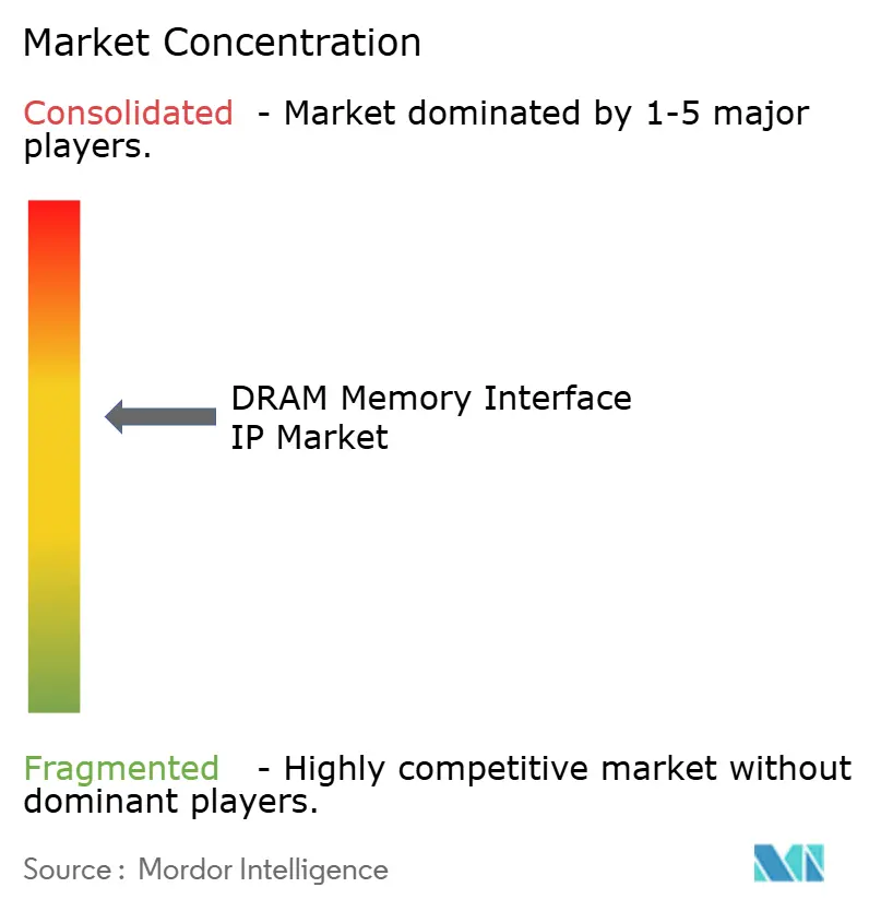
| Market Concentration | Medium |
Major Players *Disclaimer: Major Players sorted in no particular order Image © Mordor Intelligence. Reuse requires attribution under CC BY 4.0. | |
DRAM Memory Interface IP Market Analysis by Mordor Intelligence
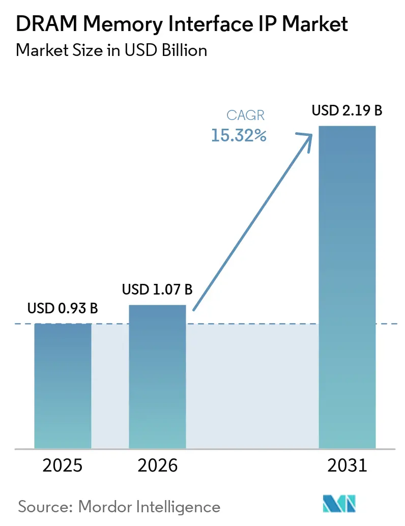
The DRAM memory interface IP market size is projected to be USD 0.93 billion in 2025, USD 1.07 billion in 2026, and reach USD 2.19 billion by 2031, growing at a CAGR of 15.32% from 2026 to 2031. The DRAM memory interface IP market is expanding because AI accelerator tape-outs, hyperscaler custom silicon programs, and the shift toward HBM4, LPDDR6, and GDDR7 have raised the cost of developing advanced interfaces internally. The gap between what newer JEDEC standards require and what product teams can deliver within tighter tape-out windows has made pre-verified, silicon-proven IP the more practical choice across customer groups. The DRAM memory interface IP market is also benefiting from the move toward chiplet-based designs and advanced packaging, because memory interfaces now sit closer to the center of system performance and integration risk. That shift is changing vendor selection, with buyers placing more weight on validation depth, packaging readiness, and subsystem-level support than on standalone controller or PHY capability alone. The result is a market where leading suppliers are competing less on catalog breadth alone and more on how much schedule risk and qualification burden they can remove for customers.
Key Report Takeaways
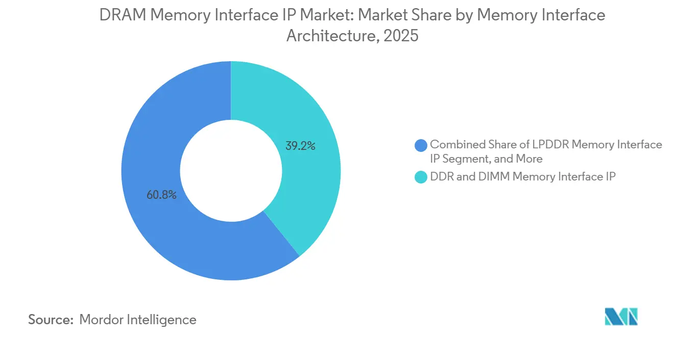
- By memory interface architecture, DDR and DIMM memory interface IP held 39.21% share of the DRAM memory interface IP market in 2025, while HBM memory interface IP is projected to expand at a 16.12% CAGR through 2031.
- By application, data centers and cloud/HPC/AI accounted for 47.91% of the dynamic random-access memory (DRAM) interface IP market in 2025 and are projected to expand at a 16.31% CAGR through 2031.
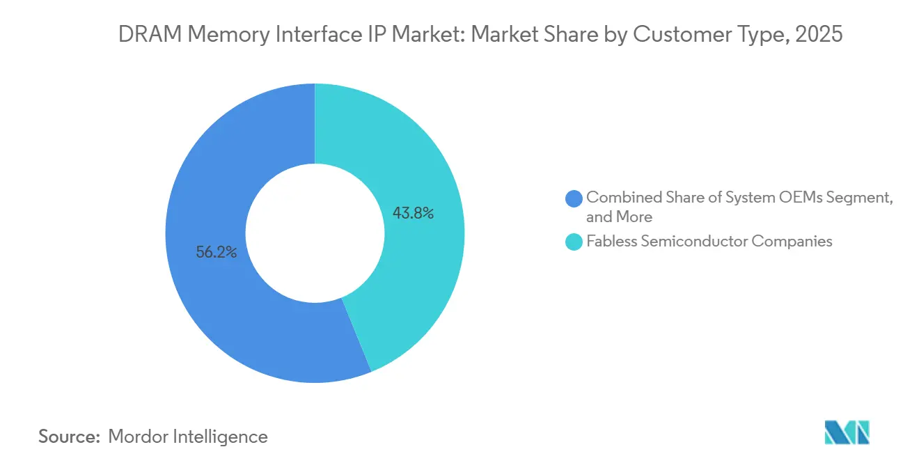
- By customer type, fabless semiconductor companies held 43.83% share in 2025, while hyperscalers are projected to record the fastest CAGR at 16.08% through 2031.
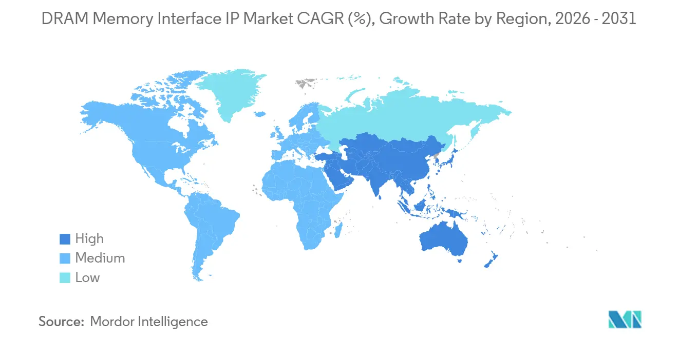
- By geography, North America held 39.51% share in 2025, while Asia-Pacific is projected to advance at a 16.28% CAGR through 2031.
Note: Market size and forecast figures in this report are generated using Mordor Intelligence’s proprietary estimation framework, updated with the latest available data and insights as of January 2026.
Global DRAM Memory Interface IP Market Trends and Insights
Driver Impact Analysis*
| Driver | (~) % Impact on CAGR Forecast | Geographic Relevance | Impact Timeline |
|---|---|---|---|
| Rising AI, HPC, and Data Center Memory Bandwidth Requirements | +5.2% | Global, with highest intensity in North America and Asia-Pacific core | Short term (≤ 2 years) |
| Migration to LPDDR5X, GDDR7, and HBM-Linked Interfaces | +3.8% | Global, Asia-Pacific core for mobile and graphics, North America for AI and data center | Short term (≤ 2 years) |
| Increasing Chiplet-Based and Advanced Package Adoption | +2.5% | Taiwan, South Korea, North America, with spillover to Japan and Europe | Medium term (2-4 years) |
| Automotive ADAS and In-Vehicle Compute Memory Complexity | +1.2% | Europe, Japan, and North America, with growing demand in China and South Korea | Medium term (2-4 years) |
| Shorter Design Cycles Favoring Pre-Verified IP Reuse | +0.9% | Global, particularly North America and Asia-Pacific fabless ecosystems | Short term (≤ 2 years) |
| Memory Security, Reliability, and Signal Integrity Demands | +0.6% | Global, most pronounced in automotive and enterprise server segments | Long term (≥ 4 years) |
| Source: Mordor Intelligence | |||
Rising AI, HPC, and Data Center Memory Bandwidth Requirements
AI training and inference workloads have made memory bandwidth a central design constraint for advanced accelerators, elevating the strategic role of the DRAM memory interface IP market. Buyers increasingly need complete controller and PHY stacks that are already silicon-proven, because in-house development no longer aligns with the timing of competitive AI programs. That requirement is especially clear in HBM programs, where subsystem validation, packaging readiness, and interoperability have become part of the buying decision rather than follow-on work. This trend is tightening the qualified vendor pool in the dynamic random-access memory (DRAM) memory interface IP market, because only a few suppliers can support large AI and HPC deployments with proven platforms. Synopsys validated an HBM4 IP test chip at 9.2Gbps on a 3nm process in February 2026, and Rambus launched HBM4E controller IP rated up to 16Gbps per pin in March 2026, showing how strongly AI memory requirements are shaping current product roadmaps.
Migration To LPDDR5X, GDDR7, and HBM-Linked Interfaces
The move to LPDDR6, GDDR7, and newer HBM generations is creating a broad replacement cycle across mobile, graphics, AI, and server programs in the DRAM memory interface IP market. JEDEC presented LPDDR6 features in 2025 with data rates up to 14.4Gbps per pin and wider channel structures, which means suppliers need more than a minor PHY revision to stay current.[1]JEDEC, “LPDDR6 Power Supply, Interface, and Reliability Features,” JEDEC, jedec.org Cadence launched an LPDDR6/5X 14.4Gbps memory IP system solution in July 2025, which linked new standard adoption directly to commercial IP availability. This pace is forcing vendors in the DRAM memory interface IP market to maintain multiple development tracks simultaneously, increasing R&D pressure and favoring suppliers with deeper platform resources. It also changes customer timing, because many buyers now prefer to lock in next-generation IP earlier to avoid getting trapped between one standard transition and the next.
Increasing Chiplet-Based and Advanced Package Adoption
Chiplet-based design is changing how memory interface IP is specified, tested, and sold in the DRAM market. HBM4 routing demands and package-level signal density mean that interface delivery now depends as much on interposer and package behavior as it does on die-level design. Siemens EDA noted that HBM4 requires extreme wiring density and close package co-design, which makes advanced 2.5D integration central to successful deployment. Synopsys reinforced that direction with its February 2026 HBM4 test chip validation, which showed that production-ready interface development is already moving alongside advanced process and packaging readiness. As a result, the DRAM memory interface IP market is moving toward bundled offerings that include models, reference flows, and package-aware validation support, rather than isolated IP blocks.
Automotive ADAS and In-Vehicle Compute Memory Complexity
Automotive compute is becoming a more serious growth lane for the DRAM memory interface IP market as bandwidth needs rise in ADAS and software-defined vehicle platforms. JEDEC stated that advanced automotive AI systems can require 300GB/s to 500GB/s of bandwidth, which pushes vehicle programs toward LPDDR5X now and more advanced memory options over time. The automotive path is more challenging than the data center path because qualification cycles are longer and safety requirements are stricter, especially for ISO 26262 and ASIL-D. Cadence also highlighted chiplet-based physical AI bring-up work for automotive ADAS and robotics, indicating that automotive programs are already integrating memory and I/O into more complex architectures. That widens the addressable scope of the DRAM memory interface IP market, but it also increases the technical and contractual burden on suppliers seeking to qualify for automotive design wins.
Restraint Impact Analysis*
| Restraint | (~) Impact on CAGR Forecast | Geographic Relevance | Impact Timeline |
|---|---|---|---|
| High NRE and Validation Cost for Advanced Memory Interfaces | -1.8% | Global, most severe for Tier-2 fabless companies in North America, Europe, and Asia-Pacific | Short term (≤ 2 years) |
| Limited Customer Base and Long Qualification Cycles | -1.2% | Global, particularly constraining in automotive in Europe and Japan and enterprise server in North America | Medium term (2-4 years) |
| Rapid DRAM Standard Evolution Risking IP Obsolescence | -0.9% | Global, with highest exposure in mobile and graphics segments | Medium term (2-4 years) |
| Integration Complexity Across Process Nodes and Packages | -0.6% | Asia-Pacific advanced packaging hubs, with spillover to North America chiplet ecosystems | Long term (≥ 4 years) |
| Source: Mordor Intelligence | |||
High NRE and Validation Cost for Advanced Memory Interfaces
High development and validation costs remain the clearest brake on the DRAM memory interface IP market, especially at advanced nodes and in HBM programs. The technical burden now extends beyond controller and PHY design into package interaction, interoperability work, and deep characterization across multiple operating conditions. Synopsys's HBM4 validation milestone and GUC's 12Gbps HBM4 demonstration on TSMC's 3nm with CoWoS show the engineering depth required before commercial deployment becomes credible.[2]Synopsys, “World's First HBM4 IP Test Chip, Early Silicon Validation for Next-Generation AI and HPC,” Synopsys, synopsys.com That cost structure narrows the pool of customers that can quickly adopt the most advanced IP, and it also narrows the pool of vendors that can fund development across successive standards. In practical terms, the DRAM memory interface IP market continues to grow, but its highest-value tiers remain easier for large vendors and well-capitalized buyers to access than for smaller entrants.
Limited Customer Base and Long Qualification Cycles
The DRAM memory interface IP market serves a concentrated set of buyers, including hyperscalers, large fabless companies, automotive SoC suppliers, and graphics-focused chip developers. That means each large program matters, and a delayed or lost design-in can have a visible effect on supplier revenue momentum. The challenge is sharper in automotive and enterprise programs, where qualification windows often stretch across several years and can outlast the commercial peak of a given interface generation. Rambus said in March 2026 that it had accumulated more than 100 HBM design wins, which shows how prior qualification history can compound into a durable advantage when customers prefer vendors with proven integration records. This dynamic supports incumbents in the dynamic random-access memory (DRAM) memory interface IP market, because existing validation depth and customer trust matter almost as much as raw technical capability.
*Our forecasts treat driver/restraint impacts as directional, not additive. The impact forecasts reflect baseline growth, mix effects, and variable interactions.
Segment Analysis
By Memory Interface Architecture: HBM Gains Momentum As AI Silicon Raises Bandwidth Demands
DDR and DIMM memory interface IP held 39.21% of the DRAM memory interface IP market share in 2025, supported by the broad installed base of DDR5 and MRDIMM interfaces in cloud, enterprise, and AI server systems. This part of the DRAM memory interface IP market remained active because server platforms continued to upgrade memory bandwidth without abandoning the familiar DDR ecosystem. Cadence reinforced that demand in April 2025 when it introduced a DDR5 12.8Gbps MRDIMM Gen2 memory IP system solution on TSMC N3 for AI cloud and enterprise data center deployments. LPDDR also continued to expand its relevance beyond handsets, as newer standards are now tied to automotive compute, edge AI, and low-power server memory applications.
JEDEC's 2025 LPDDR6 materials showed a move to 14.4 Gbps per pin and broader channel structures, opening a new development cycle for suppliers serving mobile and inference workloads. Cadence followed that transition with its LPDDR6/5X system solution, showing how quickly standards activity is translating into product launches. HBM memory interface IP is projected to grow at a 16.12% CAGR through 2031, making it the fastest-growing architecture in the DRAM memory interface IP market as AI accelerators and GPU programs move into HBM4 and HBM4E cycles. Rambus introduced HBM4E controller IP in March 2026, and GUC demonstrated a 12Gbps HBM4 platform in April 2026, which shows that HBM is becoming a broader subsystem opportunity that includes controller logic, PHY design, package support, and simulation collateral.


By Application: AI Infrastructure Continues To Pull The Largest Demand Pool
Data centers and cloud/HPC/AI accounted for 47.91% of the DRAM memory interface IP market in 2025 and are projected to expand at a 16.31% CAGR through 2031. This combination of the largest share and fastest growth shows how strongly AI infrastructure spending is shaping the DRAM memory interface IP market. Buyers in this segment place the highest value on fully characterized memory subsystems, because accelerator schedules leave little room for internal interface redesign once the architecture is set. Synopsys's LPDDR6/5X/5 PHY portfolio and its HBM4 validation work show how vendors are building product families that can serve both high-bandwidth AI training systems and power-sensitive inference platforms.
Mobile and consumer devices remained the next major demand base, with LPDDR5X and LPDDR6 adoption supporting flagship handsets, AI-on-device functions, and compact edge modules. Graphics and gaming also stayed important, because GDDR-class interfaces remain central to high-performance rendering and AI-assisted graphics workloads. Automotive and ADAS are gaining weight in the DRAM memory interface IP market as vehicle compute platforms demand more bandwidth and stronger functional safety support. JEDEC's automotive guidance and Cadence's chiplet bring-up work for ADAS and robotics both point to a future in which automotive memory IP must be both higher-performing and more thoroughly validated. Industrial, IoT, and networking programs remained smaller, but they continued to support steady demand for the reuse of mature-node DDR4 and LPDDR4X, where cost control and process portability still matter.
By Customer Type: Hyperscaler Programs Push Licensing Toward Deeper Co-Development
Fabless semiconductor companies held a 43.83% share in 2025, making them the largest customer group in the DRAM memory interface IP market. Their position reflects a practical dependence on licensed interface IP, because many fabless firms do not maintain the analog, verification, and packaging resources needed to develop these interfaces internally at leading-edge speeds. This customer base remains attractive for suppliers because it spans AI accelerators, networking SoCs, mobile chipsets, and several multi-generation product families. At the same time, IDMs stayed selective in their buying behavior, using external IP more often for standard interfaces or for programs where time risk outweighed the benefit of in-house development.
Hyperscalers are projected to grow at a 16.08% CAGR through 2031, making them the fastest-expanding customer type in the DRAM memory interface IP market. Their shift toward custom AI silicon is changing commercial practice, because vendors now need to offer subsystem-level packages and closer engineering involvement rather than just catalog licensing. Rambus made its HBM4E controller IP available for early-access licensing and pairing with third-party PHY solutions, which reflects the kind of flexible engagement model these customers increasingly expect. Synopsys also extended its position across both memory and die-to-die connectivity paths in 2026, which aligns with customer demand for broader interface platforms in chiplet-based compute programs. System OEMs remained smaller in share, but they continued to grow as risk-sensitive buyers in automotive and infrastructure programs where schedule certainty is often worth more than interface ownership.
Geography Analysis
North America held 39.51% of the DRAM memory interface IP market share in 2025, making it the largest regional contributor. The region benefits from a dense mix of hyperscalers, AI chip developers, and major platform IP vendors, which gives it unusually strong design activity at the advanced end of the market. Synopsys, Cadence, and Rambus continue to shape a large share of the high-value pipeline from North America through their leadership in HBM, DDR, and LPDDR platforms.[3]Cadence Design Systems, “Cadence Introduces Industry-First LPDDR6/5X 14.4Gbps Memory IP to Power Next-Generation AI Infrastructure,” Cadence, cadence.com North American programs also tend to support higher-value, longer-duration contracts because many are tied to custom AI silicon and large cloud infrastructure roadmaps. That keeps the DRAM memory interface IP market especially deep in this region, even when buyer counts remain limited.
Europe maintained a distinct position through automotive semiconductor demand and safety-driven qualification requirements. Automotive suppliers in the region need memory interfaces that can satisfy both higher in-vehicle bandwidth and long product life cycles, which support ongoing demand for qualified LPDDR and future GDDR solutions. JEDEC's automotive guidance makes clear that higher-performance memory is becoming necessary for advanced vehicle AI systems, while compliance expectations remain stringent. Europe also contributes to the supply side through design and verification capabilities linked to advanced packaging workflows. Siemens EDA's HBM packaging guidance shows how memory interface planning is increasingly tied to system and package co-design, which adds to Europe's role in enablement even when direct licensing scale is lower than in North America.
Asia-Pacific is projected to grow at a 16.28% CAGR through 2031, making it the fastest-growing geography in the DRAM memory interface IP market. Taiwan and South Korea remain central because advanced packaging and HBM production are heavily concentrated in these markets. GUC's HBM4 demonstration on TSMC 3nm with CoWoS reflects Taiwan's role in bringing the latest packaging-linked memory interfaces closer to production. South Korea is also becoming more visible on the IP supply side, as OPENEDGES signed its first commercial license for LPDDR6 and LPDDR5X memory subsystem IP in April 2026. China is pushing localization in memory interface IP, and Innosilicon's first domestic LPDDR6 and LPDDR5X combo PHY and controller delivery in January 2026 marked a notable step in that direction. Japan remains important through automotive and industrial demand, while the rest of the world continues to expand gradually through design services and integration support tied to the wider Asia-Pacific supply chain.

Competitive Landscape
The DRAM memory interface IP market is moderately concentrated at the advanced end and more fragmented across legacy and mid-market interfaces. Synopsys and Cadence hold the broadest multi-standard portfolios, giving them strong positions in programs that require DDR5, LPDDR6, GDDR-class, and HBM-class support from a small number of suppliers. Rambus remains more specialized, but its HBM controller franchise and long list of design wins give it a durable place in the highest-bandwidth part of the market.[4]Rambus Inc., “Rambus Sets New Benchmark for AI Memory Performance with Industry-Leading HBM4E Controller IP,” Rambus, rambus.com This structure means the DRAM memory interface IP market rewards validation depth and ecosystem integration more than low-cost entry alone. It also helps explain why challengers often win first in targeted niches rather than across full platform portfolios.
Recent strategic moves show how leading vendors are trying to defend or extend that position. Synopsys used its February 2026 HBM4 test chip validation to raise the proof threshold for HBM deployments at the production path. Rambus followed in March 2026 with HBM4E controller IP that could be paired with third-party PHY solutions, which widened its relevance in subsystem deals rather than controller-only sales. Cadence had already strengthened its reach in 2025 with industry-first LPDDR6 and DDR5 MRDIMM launches aimed at AI infrastructure and cloud deployments. These moves show that competitive advantage in the DRAM memory interface IP market increasingly comes from being present at every step of a customer's memory roadmap.
Challengers are still finding space where incumbent portfolios do not fully match local needs or newer design styles. Alphawave Semi demonstrated a 9.2Gbps HBM3E subsystem delivering 1.2TB/s in 2024, positioning it as a serious challenger in AI and HPC memory connectivity. OPENEDGES and Innosilicon also reflect a broader trend toward regional and foundry-aligned suppliers moving up the value chain in LPDDR and related memory subsystems. Siemens EDA is shaping the competitive setting from the workflow side by embedding HBM and package co-design know-how into implementation and verification paths. That keeps the dynamic random-access memory (DRAM) memory interface IP market open to new entrants in specific pockets, even though the highest-value programs still favor vendors with broad validation histories and deep ecosystem ties.
DRAM Memory Interface IP Industry Leaders
Synopsys, Inc.
Cadence Design Systems, Inc.
Rambus Inc.
Alphawave IP Group plc
Arm Limited
- *Disclaimer: Major Players sorted in no particular order

Recent Industry Developments
- May 2026: Rambus announced its complete DDR5 9600 Client Memory Module Chipset for CUDIMM, CQDIMM, and CSODIMM modules targeting next-generation AI PCs. The chipset includes a new Gen2 Client Clock Driver (CKD02) supporting DDR5 operation up to 9600 MT/s, along with a Power Management IC and SPD Hub, delivering a fully integrated module solution for AI workstation and notebook platforms.
- April 2026: Rambus launched its SOCAMM2 Server Module Chipset, enabling low-power LPDDR5X-based memory modules for AI server platforms. The chipset supports JEDEC-standard LPDDR5X SOCAMM2 modules at up to 9.6 Gb/s and includes an SPD Hub and voltage regulators designed to replace soldered LPDDR with detachable, upgradable server modules.
- April 2026: GUC demonstrated a 12 Gbps HBM4 IP platform implemented on TSMC's 3nm process with CoWoS advanced packaging at the TSMC 2026 North America Technology Symposium. The platform integrates GUC's full-functional HBM4 controller and PHY IP with HBM4 memory, with GUC reporting that its prior-generation HBM3E IP achieved speeds 15% above specification in production.
- April 2026: OPENEDGES Technology announced its first commercial license agreement for memory subsystem IP supporting both LPDDR6 and LPDDR5X standards simultaneously, targeting next-generation AI and HPC SoC customers. This represented the first commercial LPDDR6 IP licensing deal executed by a Korean IP vendor and marks South Korea's emergence as an IP supply source alongside its established role as a DRAM device manufacturer.


Global DRAM Memory Interface IP Market Report Scope
The DRAM Memory Interface IP market comprises the licensing, development, and commercialization of semiconductor intellectual property (IP) cores that enable reliable communication between system-on-chip (SoC), processor, ASIC, FPGA, or accelerator devices and dynamic random-access memory (DRAM) technologies. These IP solutions incorporate memory controllers, physical layer (PHY) interfaces, protocol logic, training algorithms, signal integrity features, and related design components required to support high-speed DRAM standards.
The DRAM Memory Interface IP Report is Segmented by Memory Interface Architecture (DDR and DIMM Memory Interface IP, LPDDR Memory Interface IP, GDDR Memory Interface IP, and HBM Memory Interface IP), Application (Data Center/Cloud/HPC/AI, Mobile and Consumer Devices, Graphics/Gaming, Automotive/ADAS, and Industrial/IoT/Networking), Customer Type (Fabless Semiconductor Companies., IDMs, System OEMs, and Hyperscalers), and Geography (North America, Europe, Asia-Pacific, and Rest of World). The Market Forecasts are Provided in Terms of Value (USD).
| DDR and DIMM Memory Interface IP |
| LPDDR Memory Interface IP |
| GDDR Memory Interface IP |
| HBM Memory Interface IP |
| Data Center/Cloud/HPC/AI |
| Mobile and Consumer Devices |
| Graphics/Gaming |
| Automotive/ADAS |
| Industrial/IoT/Networking |
| Fabless Semiconductor Companies |
| IDMs |
| System OEMs |
| Hyperscalers |
| North America | |
| Europe | |
| Asia-Pacific | China |
| Japan | |
| South Korea | |
| Taiwan | |
| Rest of Asia-Pacific | |
| Rest of the World |
| By Memory Interface Architecture | DDR and DIMM Memory Interface IP | |
| LPDDR Memory Interface IP | ||
| GDDR Memory Interface IP | ||
| HBM Memory Interface IP | ||
| By Application | Data Center/Cloud/HPC/AI | |
| Mobile and Consumer Devices | ||
| Graphics/Gaming | ||
| Automotive/ADAS | ||
| Industrial/IoT/Networking | ||
| By Customer Type | Fabless Semiconductor Companies | |
| IDMs | ||
| System OEMs | ||
| Hyperscalers | ||
| By Geography | North America | |
| Europe | ||
| Asia-Pacific | China | |
| Japan | ||
| South Korea | ||
| Taiwan | ||
| Rest of Asia-Pacific | ||
| Rest of the World | ||


Key Questions Answered in the Report
What is the current and forecast value of the DRAM memory interface IP market?
The DRAM memory interface IP market was valued at USD 0.93 billion in 2025, is valued at USD 1.07 billion in 2026, and is forecast to reach USD 2.19 billion by 2031 at a 15.32% CAGR.
Which application area generates the highest demand for DRAM memory interface IP?
Data center and cloud/HPC/AI led with 47.91% share in 2025 and is also the fastest-growing application at a 16.31% CAGR through 2031.
Why is HBM becoming more important in DRAM memory interface IP?
HBM is tied closely to AI accelerators and high-performance compute systems that need extreme bandwidth, which is why the HBM architecture segment is projected to grow at a 16.12% CAGR through 2031.
Which customer group is expanding fastest in this field?
Hyperscalers are the fastest-growing customer type with a 16.08% CAGR, driven by their shift toward custom AI silicon and deeper co-development with IP vendors.
Which region leads demand and which region is growing fastest?
North America held the largest share at 39.51% in 2025, while Asia-Pacific is projected to grow the fastest at a 16.28% CAGR through 2031.
What is the biggest challenge facing suppliers of advanced memory interface IP?
The main challenge is the high cost and long validation cycle tied to advanced nodes, HBM-class interfaces, and package-level integration, which limits participation to well-funded vendors and buyers.
Page last updated on:


