
DRAM IP Controller Market Size and Share
Market Overview
| Study Period | 2020 - 2031 |
|---|---|
| Market Size (2026) | USD 0.72 Billion |
| Market Size (2031) | USD 1.35 Billion |
| Growth Rate (2026 - 2031) | 13.40 % |
| Fastest Growing Market | North America |
| Largest Market | Asia-Pacific |
| Market Concentration | Medium |
Major Players *Disclaimer: Major Players sorted in no particular order Image © Mordor Intelligence. Reuse requires attribution under CC BY 4.0. | |
DRAM IP Controller Market Analysis by Mordor Intelligence
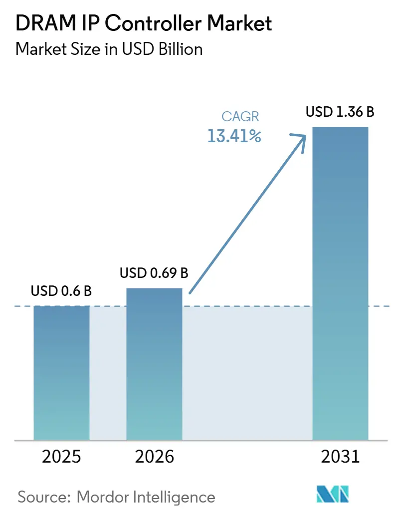
The DRAM IP controller market size is projected to be USD 0.62 billion in 2025, USD 0.72 billion in 2026, and reach USD 1.35 billion by 2031, growing at a CAGR of 13.40% from 2026 to 2031. The DRAM IP controller market is expanding as AI training systems, cloud accelerators, and high-performance computing programs keep raising bandwidth and latency requirements across new SoC designs. The shift toward DDR5 platforms and the faster move toward new LPDDR and HBM generations are creating repeated controller qualification cycles, which keeps licensing demand active even when memory pricing changes. The DRAM IP controller market is also shaped by the fact that each new SoC tape-out with an external memory interface requires fresh controller qualification, so rising design starts matter as much as rising chip output. Large hyperscalers, fabless chip companies, and ASIC design partners are pushing more custom silicon programs into the pipeline, which raises the need for silicon-proven controller IP and strong PHY, VIP, and foundry alignment. The DRAM IP controller market still faces pressure from in-house controller development at the largest cloud operators, yet the breadth of new AI, mobile, automotive, and edge compute programs continues to support third-party controller IP demand across the forecast period.
Key Report Takeaways
- By IP subsystem type, DDR Controller IP held 46.77% of the DRAM IP controller market share in 2025, while HBM Controller IP is projected to expand at a 13.87% CAGR through 2031.
- By application, Data Center/Cloud/HPC/AI accounted for 42.88% of the DRAM IP controller market size in 2025 and is projected to advance at a 13.97% CAGR through 2031.
- By customer type, fabless semiconductor companies held 44.23% share in 2025, while hyperscalers are expected to record the highest CAGR of 13.45% through 2031.
- By geography, North America represented 39.67% share in 2025, while Asia-Pacific is forecast to grow at a 13.88% CAGR through 2031.
Note: Market size and forecast figures in this report are generated using Mordor Intelligence’s proprietary estimation framework, updated with the latest available data and insights as of January 2026.
Market Trends and Insights
Drivers Impact Analysis of DRAM IP Controller Market*
| Driver | (~) % Impact on CAGR Forecast | Geographic Relevance | Impact Timeline |
|---|---|---|---|
| Rising Memory Bandwidth Demand in AI And HPC SoCs | +4.5% | Global, concentrated in North America and Asia-Pacific, Taiwan, South Korea | Short term (≤ 2 years) |
| Accelerating Transition To DDR5 and LPDDR5X Platforms | +3.0% | Global, with early adoption in North America and East Asia | Medium term (2-4 years) |
| Growing HBM Adoption in Advanced Compute Architectures | +2.5% | North America, South Korea, Taiwan | Short term (≤ 2 years) |
| Expanding Outsourced Semiconductor Design Activity | +1.5% | Asia-Pacific core, Taiwan, China, spill-over to South Asia | Medium term (2-4 years) |
| Increasing Demand for Automotive-Grade Memory Interfaces | +1.0% | Europe, Japan, North America | Long term (≥ 4 years) |
| Rising Need for Proven Multi-Protocol Controller IP | +0.8% | Global | Medium term (2-4 years) |
| Source: Mordor Intelligence | |||
Rising Memory Bandwidth Demand in AI And HPC SoCs
AI training clusters and inference accelerators require more bandwidth than earlier controller IP generations were built to handle. The DRAM IP controller market is responding through faster HBM interfaces, tighter controller latency targets, and closer controller and PHY tuning. Cadence released its HBM4 memory IP solution at 12.8Gbps in April 2025, with 20% better power efficiency and 50% better area efficiency versus HBM3E, which shows how sharply qualification thresholds have moved for leading programs.[1] Rambus launched HBM4E Controller IP in March 2026 with support for up to 16 GT/s per pin and 4.1 TB/s of bandwidth per device, which reflects the scale now required for next-generation AI accelerators. These launches show that controller competition is no longer centered on protocol support alone, because power, area, telemetry, and system-level efficiency now matter at the same time. In the DRAM IP controller market, vendors that qualify early against these AI memory demands are better placed to hold premium sockets across cloud and HPC programs.
Accelerating Transition to DDR5 And LPDDR5X Platforms
The move from DDR4 to DDR5 and from LPDDR5X toward LPDDR6 is forcing a fresh licensing cycle across server, mobile, and edge compute designs. That shift matters because older controller implementations do not transfer cleanly into new performance, reliability, and packaging requirements. Cadence launched an LPDDR5X 9600 Mbps memory IP system solution for enterprise and data center use in January 2026, integrating Microsoft's RAIDDR ECC scheme and naming Microsoft as the first customer. Synopsys stated in 2026 that LPDDR6 introduces a 24-bit channel architecture and targets data rates up to 14.4Gb/s, which turns the next mobile memory step into a full controller and PHY redesign rather than a minor update. The DRAM IP controller market benefits from this faster standards cadence because refresh cycles are arriving more quickly than in earlier DRAM generations. It also reduces the ability of customers to keep reusing DDR4-era and LPDDR5X-era controller assets across new SoC programs.
Growing HBM Adoption in Advanced Compute Architectures
HBM adoption is reshaping the DRAM IP controller market because each new HBM generation requires fresh qualification rather than a light revision of an older block. AI accelerators, advanced GPUs, and custom compute ASICs all raise the value of HBM controller IP because each design can attach multiple HBM stacks and requires very high sustained throughput. GUC demonstrated a 12Gbps HBM4 IP platform on TSMC 3nm in April 2026, with 2.5x bandwidth, 1.5x power efficiency improvement, and 2x area efficiency improvement compared with its HBM3E generation. Rambus followed with HBM4E Controller IP in March 2026, offering early-access licensing for a controller built for next-generation AI accelerators and GPUs.[2] These launches indicate that the supplier pool narrows as packaging, bandwidth, and validation requirements move higher at each HBM step. The DRAM IP controller market therefore rewards vendors that can pair controller design with advanced packaging awareness, system validation depth, and proven interoperability at leading nodes.
Expanding Outsourced Semiconductor Design Activity
Custom silicon programs and chiplet-based designs are sending more implementation work toward ASIC design service firms and platform partners. In the DRAM IP controller market, those firms act as an important distribution layer because each outsourced SoC still needs a qualified memory controller strategy. GUC's April 2026 HBM4 platform on TSMC 3nm shows how a design service company can combine memory IP, packaging readiness, and foundry alignment in one offer.[3] Alphawave Semi taped out a 64Gbps UCIe IP subsystem on TSMC 3nm in September 2025, showing how chiplet interconnect planning is now increasingly tied to memory subsystem decisions in AI and data center designs. This operating model favors vendors that can package controller IP, PHY IP, verification support, and implementation know-how into a single customer program. It also broadens the effective demand base of the DRAM IP controller market beyond standalone IP buyers and into service-led silicon development channels.
Restraints Impact Analysis of DRAM IP Controller Market*
| Restraint | (~) % Impact on CAGR Forecast | Geographic Relevance | Impact Timeline |
|---|---|---|---|
| Long Verification and Silicon Validation Cycles | -1.8% | Global | Short term (≤ 2 years) |
| High Switching Cost Between Qualified IP Vendors | -1.2% | Global, most pronounced in North America and East Asia | Medium term (2-4 years) |
| Design Complexity Across Multiple DRAM Standards | -0.8% | Global | Medium term (2-4 years) |
| Dependency on Foundry, EDA, and PHY Ecosystem Readiness | -0.9% | Asia-Pacific, Taiwan, South Korea, North America | Long term (≥ 4 years) |
| Source: Mordor Intelligence | |||
Long Verification and Silicon Validation Cycles
High-speed DRAM controller qualification still moves through RTL simulation, gate-level checks, physical implementation, silicon bring-up, and system-level validation before production use. That process can stretch across 18 to 24 months, which slows how quickly the DRAM IP controller market can absorb new entrants. The long timeline also shortens the revenue window for each controller generation before the next DRAM standard starts another refresh cycle. Buyers respond by preferring vendors with silicon-proven libraries and proven node-level experience, which raises the practical barrier for challengers even when technical capability is improving. Hyperscalers and fabless companies are starting joint testbench work earlier in the design phase, but that can lock vendor choices sooner rather than making the market more open.
High Switching Cost Between Qualified IP Vendors
Once a vendor is qualified in a live SoC program, replacing that controller means new simulation work, new physical implementation, and another full silicon validation path. The burden rises further when the controller is tied to proprietary PHY IP, VIP, and workflow dependencies from the same supplier. In the DRAM IP controller market, this makes mid-program vendor changes costly even when a second source is technically available. It also means rapid standard transitions often favor incumbents, because verification overhead is highest at the very start of a new memory generation. Revenue concentration can therefore rise during technology resets, even while buyers publicly push for more optionality.
*Our forecasts treat driver/restraint impacts as directional, not additive. The impact forecasts reflect baseline growth, mix effects, and variable interactions.
DRAM IP Controller Market Segment Analysis
By IP Subsystem Type:
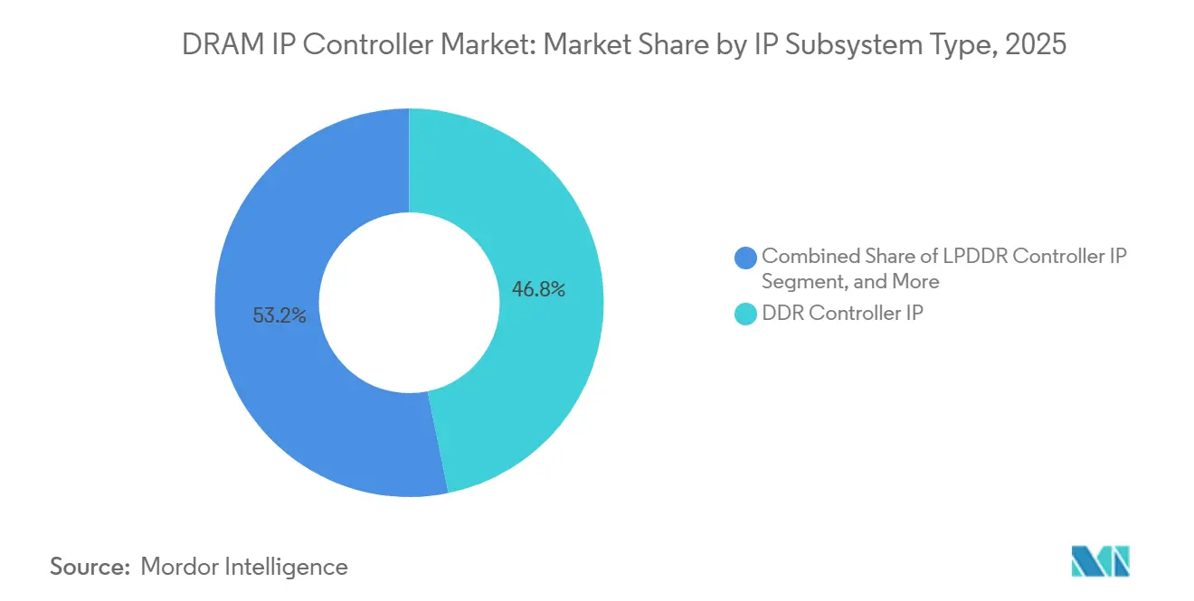
DDR Holds Ground as HBM Reshapes the Growth CurveDDR Controller IP accounted for 46.77% of the DRAM IP controller market size in 2025, while HBM Controller IP is projected to expand at a 13.87% CAGR through 2031. DDR remains the largest subsystem because server and client platforms still span a broad installed base and because the DDR5 transition is not complete across enterprise compute and PCs. That broad platform reach keeps qualification demand active across many SoC programs that cannot reuse DDR4-era controller silicon without fresh redesign. HBM is the fastest-growing subsystem because AI accelerators increasingly attach multiple memory stacks, which raises controller intensity on each new design. Cadence and Rambus both moved aggressively in this area with next-generation HBM announcements, underscoring how the DRAM IP controller market is shifting toward higher-value, performance-led sockets.
LPDDR remains an important part of the DRAM IP controller market because mobile, edge, and low-power compute programs continue to refresh on short product cycles. Synopsys highlighted LPDDR6 support up to 14.4Gb/s on a 24-bit channel architecture in 2026, which points to a new redesign cycle instead of an incremental extension of LPDDR5X assets. GDDR stays narrower in volume, but it remains strategically important because discrete GPU programs still require fresh controller qualification at rising speeds. GUC's 12Gbps HBM4 demonstration on TSMC 3nm also shows how vendors must now prove bandwidth, power, and area gains together to stay relevant in premium memory subsystems. In the DRAM IP controller industry, scale still sits with DDR, but value capture is moving toward HBM and the next wave of low-power mobile memory interfaces.

By Application:
Data Center Concentration Signals Both Strength and ExposureData Center/Cloud/HPC/AI captured 42.88% of the DRAM IP controller market size in 2025 and is projected to grow at a 13.97% CAGR through 2031. That segment leads on both share and growth because AI infrastructure spending has moved ahead of other end markets in both urgency and design complexity. Cadence launched the industry's first LPDDR5X 9600 Mbps memory IP system solution for enterprise and data center use in January 2026, and Microsoft was named as the first customer, which highlights how server-class reliability features are moving into memory interfaces that were once seen as mobile-centric. Graphics and gaming remain smaller than cloud AI in aggregate demand, but discrete GPU programs still matter because they carry high-value memory requirements and repeated qualification work. Mobile and consumer devices continue to provide a steady flow of LPDDR controller relicensing because handset and connected device refresh cycles remain frequent across the DRAM IP controller market.
Automotive and ADAS remain smaller today, but they carry long-term strategic value because centralized vehicle compute architectures need qualified LPDDR5X and DDR5 interfaces. SK hynix announced in January 2026 that its LPDDR5X automotive DRAM received ISO 26262 ASIL-D certification, which reinforces how functional safety has become a gating requirement for memory subsystems in automotive compute. That development raises the qualification bar for controller IP vendors because SoC teams will expect memory controllers to align with the same safety path as the memory devices they target. Industrial, IoT, and networking applications still contribute base-load demand through DDR4 and LPDDR4X programs, which helps offset part of the volatility seen in AI and consumer design cycles. In the DRAM IP controller market, the application mix supports both premium AI-led growth and steadier embedded licensing demand.
By Customer Type:
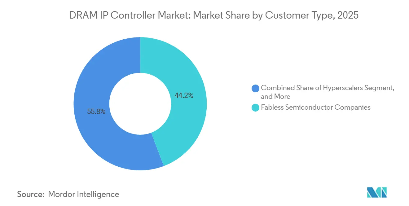
Fabless Design Wins Anchor Revenue As Hyperscalers Accelerate FastestFabless semiconductor companies held the largest share at 44.23% in 2025, while hyperscalers are forecast to grow at a 13.45% CAGR through 2031. Fabless companies remain the broadest demand base because they span AI accelerators, mobile SoCs, networking ASICs, and automotive processors, all of which need memory controller qualification in each new design cycle. Hyperscalers are expanding fastest because Google, AWS, Meta, and Microsoft are pushing more custom silicon into production roadmaps with proprietary memory requirements. That trend supports the DRAM IP controller market, but it also introduces a clear pressure point because some of the largest cloud buyers are developing controller logic internally for critical programs. Even so, the complexity of HBM4, DDR5, and advanced-node validation keeps many programs tied to external PHY IP, verification IP, and ecosystem support.
IDMs continue to provide a stable licensing base, especially in processor and server chipset designs where memory interfaces remain a core part of platform performance. System OEMs form a smaller direct customer group, but their presence is growing as cloud and infrastructure buyers push further into in-house chip development. Chiplet adoption is also changing commercial models because controller IP and PHY IP can now be licensed more separately and assembled through die-to-die standards. Alphawave Semi's 64Gbps UCIe tapeout on TSMC 3nm reflects how die-to-die interconnect planning is becoming more closely linked with memory subsystem architecture in advanced silicon programs. In the DRAM IP controller industry, customer growth is strongest where silicon ownership is moving closer to the end user and where memory architecture is becoming a direct design differentiator.
Geography Analysis
North America DRAM IP Controller Market
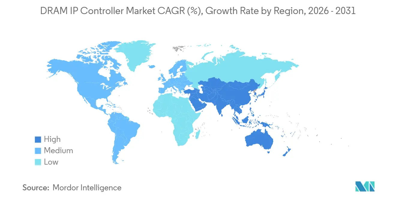
North America held 39.67% of the DRAM IP controller market share in 2025. The region remains the largest because it houses the headquarters and major design centers of leading hyperscalers, top AI accelerator companies, and the largest merchant IP suppliers. The North American commercial model also supports higher revenue per design because licensing agreements often include royalties and upfront NRE elements rather than only flatter fee structures. U.S. export controls have added another layer of support by pushing domestic buyers to deepen custom ASIC activity within U.S.-aligned supply chains. That combination gives the DRAM IP controller market a durable demand base in North America through both design concentration and higher-value deal structures.
APAC DRAM IP Controller Market
Asia-Pacific is projected to expand at a 13.88% CAGR through 2031. Taiwan remains central to the DRAM IP controller market because advanced SoCs continue to tape out at TSMC nodes, which makes early process qualification a major competitive advantage. GUC's April 2026 demonstration of a 12Gbps HBM4 platform on TSMC 3nm reflects the region's close link between design services, packaging, and leading-edge memory subsystem work. South Korea supports the region through strong HBM and advanced memory development, and SK hynix's January 2026 ASIL-D announcement also showed the depth of qualification capability around advanced memory products. China is adding competitive pressure through domestic memory IP localization efforts, while Japan contributes through automotive and edge compute memory subsystem demand.
Europe and India DRAM IP Controller Market
Europe holds a smaller position in the DRAM IP controller market, but its role is strategically important because of the automotive semiconductor chain. Qualification standards such as ISO 26262 and the growing focus on SOTIF create high entry barriers, which supports a smaller but durable pool of approved suppliers. Germany, the Netherlands, and Sweden remain key design locations, while companies such as Infineon, NXP, and STMicroelectronics support steady automotive-grade memory controller demand. Rest of the World remains modest in near-term revenue, but sovereign AI buildouts and India's growing fabless and ASIC ecosystem are expected to add design-start activity after 2027.
Competitive Landscape
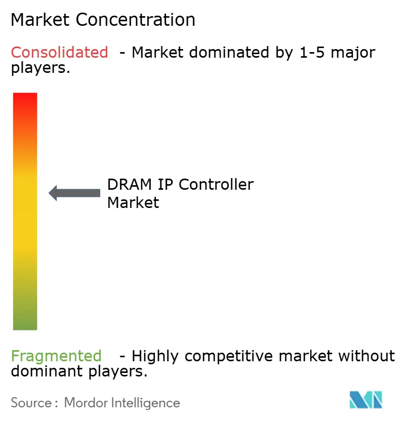
The DRAM IP controller market is moderately concentrated at the top tier, where Synopsys, Cadence, and Rambus hold the strongest positions in advanced controller licensing. Their advantage comes from broad process-node qualifications, deep EDA alignment, and bundled controller, PHY, and verification offerings that are difficult for smaller suppliers to match. Rambus launched HBM4E Controller IP in March 2026 with support for up to 16 GT/s per pin and 4.1 TB/s per device, illustrating how leaders are pushing performance ceilings to secure the next generation of AI memory sockets. Cadence released its HBM4 memory IP solution at 12.8Gbps in April 2025, validated on a full-featured TSMC N3 and N2 test chip, which shows how early foundry alignment turns technical timing into commercial leverage. In the DRAM IP controller market, being first to qualify on a new node or memory generation often matters as much as raw protocol support.
The tier-two layer is gaining credibility, especially in Asia-Pacific, where domestic qualification needs and sourcing preferences are creating room for alternative suppliers. GUC, Faraday, VeriSilicon, Innosilicon, and OPENEDGES are the names most closely associated with that competitive pressure in the current DRAM IP controller market. GUC's HBM4 platform on TSMC 3nm delivered 2.5x bandwidth, 1.5x power efficiency improvement, and 2x area efficiency improvement relative to HBM3E, which strengthens its position in advanced ASIC service engagements. That kind of proof point matters because many buyers now want a partner that can align controller IP with packaging, foundry, and implementation support rather than supply a block in isolation. The clearest white space remains in automotive and industrial use cases, where safety, lifecycle support, and qualification discipline can matter more than maximum headline speed.
Strategic differentiation is also moving toward observability, resilience, and subsystem integration rather than protocol compliance alone. Rambus built RAS and telemetry features into its HBM4E Controller IP, showing that hyperscaler and AI buyers want controller visibility that supports fleet-scale operations as well as bandwidth. Alphawave Semi taped out a 64Gbps UCIe IP subsystem on TSMC 3nm in September 2025, which shows how memory-adjacent connectivity can widen a vendor's strategic position in advanced compute designs. The DRAM IP controller market remains open to specialists, but the leaders still control the highest-value sockets because they combine controller IP with broader implementation ecosystems, early validation access, and stronger customer lock-in.
DRAM IP Controller Industry Leaders
-
Synopsys, Inc.
-
Rambus Inc.
-
Cadence Design Systems, Inc.
-
Arm Limited
-
Qualcomm Incorporated
- *Disclaimer: Major Players sorted in no particular order
DRAM IP Controller Market Companies Covered in this Report
- Synopsys, Inc.
- Cadence Design Systems, Inc.
- Rambus Inc.
- Arm Limited
- Qualcomm Incorporated
- Ceva, Inc.
- VeriSilicon Microelectronics (Shanghai) Co., Ltd.
- GUC (Global Unichip Corp.)
- Faraday Technology Corporation
- Socionext Inc.
- Andes Technology Corporation
- Innosilicon Technology Ltd.
- Sondrel Limited
- Silicon Creations, Inc.
- eMemory Technology Inc.
- Open-Silicon, Inc.
- Lattice Semiconductor Corporation
- Imagination Technologies Limited
- Keysight Technologies, Inc.
- Achronix Semiconductor Corporation
Recent Industry Developments in DRAM IP Controller Market
- May 2026: Rambus announced its complete DDR5 9600 Client Memory Module Chipset for CUDIMM, CQDIMM, and CSODIMM modules targeting next-generation AI PCs, including a Gen2 Client Clock Driver supporting memory module operation up to 9600 MT/s alongside an integrated PMIC5120 and SPD Hub, simplifying high-performance client memory module design.
- April 2026: GUC demonstrated the industry's first 12 Gbps HBM4 IP platform on TSMC 3nm at the TSMC North America Technology Symposium, featuring an in-house full-functional HBM4 Controller and PHY integrated with TSMC CoWoS advanced packaging, delivering 2.5x bandwidth and 1.5x power efficiency compared to its HBM3E generation.
- March 2026: Rambus launched the HBM4E Memory Controller IP, described as the industry's leading solution, supporting up to 16 GT/s per pin and delivering 4.1 TB/s of memory bandwidth per device, with built-in RAS and telemetry features designed for next-generation AI accelerators and GPUs, available for licensing with early-access program.
- January 2026: Cadence launched the industry's first LPDDR5X 9600 Mbps memory IP system solution for enterprise and data center use, integrating Microsoft's RAIDDR ECC scheme, which delivers DDR5-style symbol-based ECC reliability within an LPDDR5X form factor, Microsoft was announced as the first customer.
Global DRAM IP Controller Market Report Scope
The Global DRAM IP Controller Market refers to the industry segment focused on the design, licensing, and deployment of intellectual property (IP) cores that manage and optimize the interface between Dynamic Random-Access Memory (DRAM) modules and processors or system-on-chip (SoC) architectures.
The DRAM IP Controller Market Report is Segmented by IP Subsystem Type (DDR Controller IP, LPDDR Controller IP, GDDR Controller IP, and HBM Controller IP), Application (Data Center/Cloud/HPC/AI, Mobile and Consumer Devices, Graphics/Gaming, Automotive/ADAS, Industrial/IoT/Networking, and Other Applications), Customer Type (Fabless Semiconductor Companies, IDMs, System OEMs, and Hyperscalers), and Geography (North America, Europe, Asia-Pacific, and Rest of the World). The Market Forecasts are Provided in Terms of Value (USD).
Segmentation Overview
| DDR Controller IP |
| LPDDR Controller IP |
| GDDR Controller IP |
| HBM Controller IP |
| Data Center/Cloud/HPC/AI |
| Mobile and Consumer Devices |
| Graphics/Gaming |
| Automotive/ADAS |
| Industrial/IoT/Networking |
| Other Applications |
| Fabless Semiconductor Companies |
| IDMs |
| System OEMs |
| Hyperscalers |
| North America | |
| Europe | |
| Asia-Pacific | China |
| Japan | |
| South Korea | |
| Taiwan | |
| Rest of Asia-Pacific | |
| Rest of the World |
| By IP Subsystem Type | DDR Controller IP | |
| LPDDR Controller IP | ||
| GDDR Controller IP | ||
| HBM Controller IP | ||
| By Application | Data Center/Cloud/HPC/AI | |
| Mobile and Consumer Devices | ||
| Graphics/Gaming | ||
| Automotive/ADAS | ||
| Industrial/IoT/Networking | ||
| Other Applications | ||
| By Customer Type | Fabless Semiconductor Companies | |
| IDMs | ||
| System OEMs | ||
| Hyperscalers | ||
| By Geography | North America | |
| Europe | ||
| Asia-Pacific | China | |
| Japan | ||
| South Korea | ||
| Taiwan | ||
| Rest of Asia-Pacific | ||
| Rest of the World | ||
Key Questions Answered in the Report
What is the 2026 size of the DRAM IP controller market?
The DRAM IP controller market is valued at USD 0.72 billion in 2026 and is forecast to reach USD 1.35 billion by 2031 at a 13.40% CAGR.
Which application leads demand for DRAM controller IP?
Data Center/Cloud/HPC/AI leads with 42.88% share in 2025 and is also the fastest-growing application at a 13.97% CAGR through 2031.
Why is HBM controller IP growing faster than other memory interface blocks?
HBM Controller IP is projected to grow at 13.87% through 2031 because AI accelerators and advanced GPUs need very high bandwidth and repeated qualification for each new generation.
Which customer group is creating the fastest growth in this space?
Hyperscalers are the fastest-growing customer type at a 13.45% CAGR, driven by rising in-house silicon programs at large cloud operators.
Which region is strongest for DRAM controller IP demand?
North America leads with 39.67% share in 2025, while Asia-Pacific is the fastest-growing region at a 13.88% CAGR due to strong foundry, packaging, and memory ecosystem activity.
What keeps incumbent vendors strong in DRAM controller IP?
Long validation cycles, high switching costs, and bundled controller, PHY, and verification ecosystems help leading vendors defend premium sockets even as regional challengers gain ground.