Graphene Chip Market Size and Share
Market Overview
| Study Period | 2020 - 2031 |
|---|---|
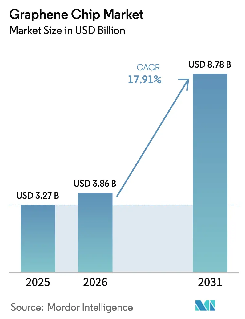
| Market Size (2026) | USD 3.86 Billion |
| Market Size (2031) | USD 8.78 Billion |
| Growth Rate (2026 - 2031) | 17.91% CAGR |
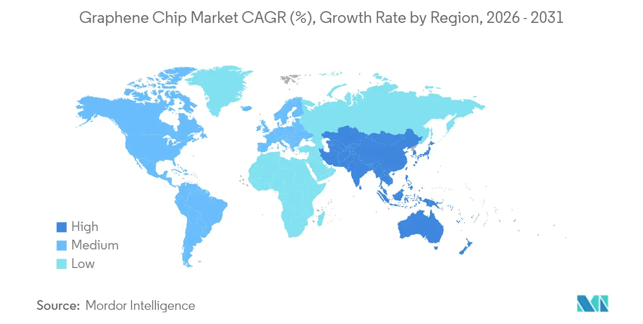
| Fastest Growing Market | Asia Pacific |
| Largest Market | Asia Pacific |
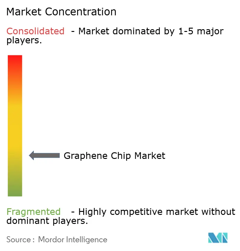
| Market Concentration | Low |
Major Players *Disclaimer: Major Players sorted in no particular order Image © Mordor Intelligence. Reuse requires attribution under CC BY 4.0. | |
Graphene Chip Market Analysis by Mordor Intelligence
Graphene chip market size in 2026 is estimated at USD 3.86 billion, growing from 2025 value of USD 3.27 billion with 2031 projections showing USD 8.78 billion, growing at 17.91% CAGR over 2026-2031. This growth reflects device makers’ need to overcome copper resistivity, silicon mobility limitations, and escalating Scope 3 emission mandates. Funding equivalent to USD 52.7 billion in the United States and EUR 43 billion (USD 47 billion) in the European Union under CHIPS-style programs is de-risking private investment in 2D semiconductor pilot lines.[1]U.S. Department of Commerce, “CHIPS and Science Act,” commerce.gov Wafer-scale chemical vapor deposition breakthroughs, combined with the Asia Pacific's leadership in 300-millimeter manufacturing, are transitioning the graphene chip from laboratory research to early commercial production. A surge in edge artificial intelligence workloads, automotive electrification above 800 volts, and flexible consumer devices further widens graphene’s performance headroom over conventional materials.
Key Report Takeaways
- By product type, integrated circuits and processors led the graphene chip market with a 38.80% revenue share in 2025, while power and energy devices are expected to advance at a 19.96% CAGR through 2031.
- By material type, CVD graphene films accounted for 43.10% of the 2025 revenue of the graphene chip market, whereas hybrid metal-graphene structures are projected to expand at a 20.12% CAGR through 2031.
- By manufacturing technology, chemical vapor deposition dominated the 2025 value of the graphene chip market, accounting for 39.30%. Liquid phase exfoliation and printing are expected to post the fastest CAGR of 20.06% from 2026 to 2031.
- By end-user industry, consumer electronics accounted for 39.85% of the revenue share in the graphene chip market in 2025, while healthcare and biomedical applications are projected to grow at a 20.95% CAGR through 2031.
- By geography, the Asia Pacific accounted for 46.10% of the 2025 revenue in the graphene chip market and is forecasted to advance at a 20.62% CAGR through 2031.
Note: Market size and forecast figures in this report are generated using Mordor Intelligence’s proprietary estimation framework, updated with the latest available data and insights as of 2026.
Global Graphene Chip Market Trends and Insights
Drivers Impact Analysis*
| Driver | (~) % Impact on CAGR Forecast | Geographic Relevance | Impact Timeline |
|---|---|---|---|
| Surging demand for ultra-fast, low-power processors in AI and edge devices | +4.2% | Global, with concentration in North America and Asia Pacific | Medium term (2-4 years) |
| Rapid maturation of wafer-scale CVD graphene film production | +3.8% | Europe and Asia Pacific, pilot lines in Germany, Netherlands, South Korea | Medium term (2-4 years) |
| Government CHIPS-style subsidies for 2D semiconductor pilot lines | +3.5% | North America, Europe, Japan, South Korea | Long term (≥4 years) |
| Adoption of graphene interconnects to overcome copper resistance bottlenecks | +2.9% | Asia Pacific (Taiwan, South Korea), North America (advanced foundries) | Long term (≥4 years) |
| Growth of flexible and wearable electronics requiring atom-thin chips | +2.6% | Global, with early adoption in consumer electronics hubs (China, South Korea, Japan) | Short term (≤2 years) |
| Semiconductor OEM shift toward eco-efficient materials for Scope-3 emissions cuts | +1.3% | Europe (stringent carbon reporting), North America (voluntary commitments) | Long term (≥4 years) |
| Source: Mordor Intelligence | |||
Surging Demand for Ultra-Fast, Low-Power Processors in AI and Edge Devices
Artificial intelligence workloads now dominate data-center and endpoint power budgets. IBM demonstrated graphene field-effect transistors switching 10,000 times faster than silicon in 2024, an advance that reduces edge inference latency to sub-nanosecond levels.[2]IBM Research, “Graphene Transistors for AI,” research.ibm.com Neuromorphic designs built on graphene memristors slash data movement by 90% because in-memory matrix multiplication eliminates the von Neumann bottleneck. Demand for battery-constrained augmented-reality headsets and autonomous robots are increasing, therefore, creates a pull market for teraops-per-watt chips that the graphene chip market can uniquely supply. Pilot deployments of analog compute tiles confirm that two-dimensional electron gases outperform bulk semiconductors by an order of magnitude in energy efficiency. Supported by CHIPS-style incentives, North American startups are expected to tape out their first silicon-graphene test chips in 2025.
Rapid Maturation of Wafer-Scale CVD Graphene Film Production
Oxygen-free CVD reactors now grow monolayer films across 300-millimeter wafers with thickness uniformity within 2%, satisfying foundry metrology rules. Europe’s 2D Experimental Pilot Line shipped multi-project wafers that integrated Hall sensors and RF transistors for 15 companies in mid-2025, providing validated process design kits and amortizing mask costs. Transfer-free batch production eliminates polymer residue, preserving carrier mobility above 10,000 cm²V⁻¹s⁻¹. Conveyor CVD systems demonstrated throughputs above 10 wafers per hour in 2024, a tenfold improvement over static chambers. These advances accelerate the transition of the graphene chip from engineering samples to risk production for sub-3-nanometer logic.
Government CHIPS-Style Subsidies for 2D Semiconductor Pilot Lines
The US CHIPS and Science Act dedicates USD 11 billion to a National Semiconductor Technology Center track that includes graphene pilot lines. Europe’s Chips Act directs EUR 43 billion (USD 47 billion) to double regional chip output by 2030, with explicit provisions for 2D material integration. Japan earmarked JPY 2 trillion (USD 13 billion) for advanced logic, with university-industry consortia focusing on epitaxial graphene on SiC substrates. South Korea set aside KRW 1 trillion (USD 750 million) for 2D materials aligned to Samsung and SK Hynix roadmaps. These subsidies help derisk capital investments in metrology tools and graphene-literate workforce training, providing the graphene chip market with a strong fiscal tailwind.
Adoption of Graphene Interconnects to Overcome Copper Resistance Bottlenecks
Copper resistivity rises sharply below 10 nanometers, degrading signal integrity. TSMC and Samsung have verified that graphene-copper hybrids cut line resistance by 30% in 7-nanometer traces, sustaining bandwidth in sub-2-nanometer nodes. Vertical graphene vias exhibit thermal conductivity above 2,000 W/m⁻¹K⁻¹, dissipating hotspots more effectively than tungsten plugs in 3D stacks. Titanium carbide contact layers and laser annealing now achieve sheet resistance below 10 Ωsq⁻¹, demonstrating a viable path to back-end-of-line integration. These gains strengthen the graphene chip market position in next-generation high-performance computing.
Restraints Impact Analysis*
| Restraint | (~) % Impact on CAGR Forecast | Geographic Relevance | Impact Timeline |
|---|---|---|---|
| High defect densities limiting device yield at 300-millimeter wafer scale | -2.8% | Global, particularly acute in high-volume fabs (Asia Pacific, North America) | Short term (≤2 years) |
| Lack of ISO-grade reliability and lifetime test standards for graphene logic | -2.1% | Global, affecting qualification at Tier-1 OEMs | Medium term (2-4 years) |
| Trade-policy volatility on critical nanocarbon supply chains | -1.6% | North America and Europe (dependent on Chinese graphite exports) | Medium term (2-4 years) |
| Limited pool of graphene-literate process engineers slowing scale-up | -1.2% | Global, with acute shortages in Europe and North America | Long term (≥4 years) |
| Source: Mordor Intelligence | |||
High Defect Densities Limiting Device Yield
CVD graphene wafers still exhibit 1,000–10,000 defects cm⁻², resulting in yields of less than 60% for Hall sensors compared to 95% for silicon MEMS. Raman microscopy reveals threshold shifts when single-atom vacancies occur, causing parametric fails in analog circuits.[3]ChemRxiv, “Raman Microscopy for GFET Arrays,” chemrxiv.org Polymer transfer processes add tears and residue. Multi-project wafer data indicate that resolving these yield gaps is the top near-term hurdle for the graphene chip market.
Lack of ISO-Grade Reliability and Lifetime Test Standards
Current ISO and JEDEC guidelines target bulk silicon failure modes. No accelerated stress tests exist for two-dimensional channels, leaving fabs unable to estimate the mean time to failure required for AEC-Q100 or MIL-STD-883 compliance. As a result, qualification cycles extend from 12 to 18 months, inflating non-recurring engineering costs and slowing procurement decisions. Industry groups, including IEEE P2800, are drafting common protocols, and once published, they are expected to improve supply-chain confidence in the graphene chip market.
*Our forecasts treat driver/restraint impacts as directional, not additive. The impact forecasts reflect baseline growth, mix effects, and variable interactions.
Segment Analysis
By Product Type: Power Devices Lead Growth Amid Electrification Push
Power and energy devices are expected to account for a 19.96% CAGR between 2026 and 2031, the highest among product categories, as automotive OEMs pair graphene heat spreaders with silicon carbide or gallium nitride dies to maintain junction temperatures below 175 °C in 800-volt drivetrains. The graphene chip market size for power devices is projected to reach USD 2.18 billion by 2031, nearly doubling its contribution by 2026. Integrated circuits and processors still held the largest 38.80% take of 2025 revenue, anchored in AI accelerators that need sub-nanosecond switching. RF and high-frequency devices follow, exploiting graphene’s terahertz transparency for 5G millimeter-wave front ends.
Sensor and MEMS chips leverage graphene’s large surface area for ppm-level gas detection, advancing predictive maintenance across smart factories. Interconnects and advanced packaging remain niche but strategic, with Samsung’s 2024 demonstration of vertical graphene vias reducing thermal resistance by 40% compared to tungsten. These innovations illustrate how the graphene chip market delivers both performance leadership and new value propositions across product lines.


By Material Type: Hybrid Structures Unlock RF Performance
CVD graphene films accounted for 43.10% of the 2025 value, as they integrate seamlessly into existing cleanrooms. Hybrid metal-graphene stacks are projected to post a 20.12% CAGR to 2031, the fastest in this grouping, as layering gold or copper with graphene reduces skin-effect losses above 10 GHz. The graphene chip market share for hybrid stacks is expected to exceed 24.60% by 2031. Graphene nanoplatelets dominate conductive inks for printed electronics, where micron-scale flakes suffice. Graphene oxide variants penetrate biosensors, attaching antibodies for the detection of sub-micromolar analytes.
Graphene nanoribbons and quantum dots open the all-important bandgap, achieving on-off ratios exceeding 10,000:1. However, yields under 20% and prices above USD 10,000 g⁻¹ restrict their application to R&D. Continued hybrid metal work promises to keep the graphene chip at the forefront of RF and analog innovation.
By Manufacturing Technology: Liquid-Phase Methods Scale Printed Electronics
Chemical vapor deposition accounted for 39.30% of 2025 manufacturing revenue, thanks to mobilities exceeding 5,000 cm²V⁻¹s⁻¹. Liquid phase exfoliation and printing, however, will exhibit the fastest 20.06% CAGR, delivering roll-to-roll throughput exceeding 10 m/min⁻¹ on flexible substrates. The graphene chip market size for printed electronics is projected to reach USD 690 million by 2031, driven by the demand for wearable patches and disposable biosensors. Epitaxial growth on SiC yields the highest quality, with mobilities approaching 100,000 cm²V⁻¹s⁻¹; however, its high-temperature steps and the cost of SiC wafers limit its applications to quantum metrology and terahertz detectors.
Plasma and laser methods offer atmospheric synthesis but introduce grain boundaries. Mechanical exfoliation remains purely academic. Progress in ink rheology and gravure press retrofits suggests printed electronics will broaden the graphene chip market beyond high-capital fabs.

By End-User Industry: Healthcare Drives Fastest Adoption
Healthcare and biomedical applications are expected to grow at a 20.95% CAGR through 2031, the fastest among end users. Continuous glucose monitors using graphene electrodes detect sub-micromolar analytes without immune reactions, while Stanford’s 2024 neural interface achieved a 10× signal-to-noise boost over platinum. Consumer electronics retained the largest 39.85% share in 2025, benefiting from laser lift-off foldable OLEDs that cut module thickness by 30%. Automotive electrification adds demand for thermal management in 800-volt inverters.
Industrial Internet-of-Things nodes exploit graphene’s part-per-billion gas sensitivity, improving air-quality monitoring. Aerospace seeks radiation-hard graphene transistors for satellites exposed to a total dose of 100 kRad. These diverse use cases ensure the graphene chip market continues to diversify its revenue base.
Geography Analysis
The Asia Pacific commanded 46.10% of the revenue in 2025 and is forecast to expand at a 20.62% CAGR, maintaining its leadership as TSMC integrates graphene interconnects into sub-2-nanometer logic. China’s 14th Five-Year Plan designates graphene a strategic material, funneling subsidies into pilot lines. South Korea and Japan fund research on 2D materials for high-bandwidth memory stacks and power modules, reinforcing their regional dominance.
North America allocates USD 11 billion for 2D materials under CHIPS, but its dependence on Chinese graphite (accounting for 70% of the global supply) raises cost exposure. Europe’s Graphene Flagship 2.0 continues to provide shared infrastructure and multi-project wafers, sustaining collaborative momentum. The Middle East, Africa, and South America remain at early adoption stages, yet they offer long-term potential as fabrication capacity globalizes. Trade-policy volatility around graphite exports underscores the need for diversified supply in the graphene chip market.

Competitive Landscape
More than 250 companies participate across synthesis, device design, and system integration, resulting in a fragmented field with no single dominant platform. Paragraf expanded Hall sensor capacity to 10,000 units per month after closing USD 19 million Series B funding.[4]Paragraf Ltd., “Hall-Effect Sensors Expansion,” paragraf.com Graphenea doubled the CVD output to 200,000 cm²/month⁻with oxygen-free reactors, reducing the defect density to below 1,000 cm⁻². NanoXplore formed a USD 15 million joint venture with Martinrea to integrate graphene thermal films in electric-vehicle battery packs.
Patent analytics reveal 76% of graphene filings originate from private enterprises rather than academia, indicating a shift toward proprietary know-how. Liquid-phase exfoliation specialists target high-volume printed sensors, thereby bypassing the capital-intensive nature of CVD fabs. IEEE P2800 reliability standards, once ratified, are expected to reduce qualification barriers and may trigger consolidation as Tier-1 OEMs seek multi-sourcing assurance. Technology differentiation increasingly hinges on achieving defect densities below 1,000 cm⁻², a threshold only a handful of players currently meet.
Graphene Chip Industry Leaders
Paragraf Limited
Graphenea S.A.
NanoXplore Inc.
Graphene Square Inc.
XG Sciences Inc.
- *Disclaimer: Major Players sorted in no particular order

Recent Industry Developments
- October 2025: TSMC partnered with the National Semiconductor Technology Center to pilot graphene interconnects for sub-2-nanometer nodes, allocating USD 50 million to infrastructure upgrades.
- September 2025: The Samsung Advanced Institute of Technology has published 100-femtojoule graphene memristors that can endure 10,000 write cycles.
- July 2025: EU 2D Experimental Pilot Line completed its third multi-project wafer run, delivering graphene Hall sensors and RF transistors to 15 companies.
- May 2025: NanoXplore and Martinrea have invested USD 15 million in graphene thermal management for electric vehicles, with the goal of achieving production by 2026.
- March 2025: Paragraf raised USD 19 million to scale Hall sensor output to 10,000 units per month by mid-2026.


Global Graphene Chip Market Report Scope
| Integrated Circuits and Processors |
| Sensor and MEMS Chips |
| RF and High-Frequency Devices |
| Power and Energy Devices |
| Interconnects and Packaging |
| CVD Graphene Films |
| Graphene Nanoplatelets |
| Graphene Oxide and rGO |
| Graphene Nanoribbons and Quantum Dots |
| Hybrid Metal-Graphene Structures |
| Chemical Vapor Deposition |
| Epitaxial Growth on SiC |
| Liquid Phase Exfoliation and Printing |
| Plasma and Laser Induced Growth |
| Others |
| Consumer Electronics |
| Automotive and Transportation |
| Industrial and IoT |
| Healthcare and Biomedical |
| Aerospace and Defense |
| Other End-user Industries |
| North America | United States | |
| Canada | ||
| Mexico | ||
| South America | Brazil | |
| Argentina | ||
| Rest of South America | ||
| Europe | Germany | |
| France | ||
| United Kingdom | ||
| Italy | ||
| Spain | ||
| Rest of Europe | ||
| Asia-Pacific | China | |
| Japan | ||
| India | ||
| South Korea | ||
| Australia | ||
| Rest of Asia-Pacific | ||
| Middle East and Africa | Middle East | United Arab Emirates |
| Saudi Arabia | ||
| Turkey | ||
| Rest of Middle East | ||
| Africa | South Africa | |
| Egypt | ||
| Rest of Africa | ||
| By Product Type | Integrated Circuits and Processors | ||
| Sensor and MEMS Chips | |||
| RF and High-Frequency Devices | |||
| Power and Energy Devices | |||
| Interconnects and Packaging | |||
| By Material Type | CVD Graphene Films | ||
| Graphene Nanoplatelets | |||
| Graphene Oxide and rGO | |||
| Graphene Nanoribbons and Quantum Dots | |||
| Hybrid Metal-Graphene Structures | |||
| By Manufacturing Technology | Chemical Vapor Deposition | ||
| Epitaxial Growth on SiC | |||
| Liquid Phase Exfoliation and Printing | |||
| Plasma and Laser Induced Growth | |||
| Others | |||
| By End-user Industry | Consumer Electronics | ||
| Automotive and Transportation | |||
| Industrial and IoT | |||
| Healthcare and Biomedical | |||
| Aerospace and Defense | |||
| Other End-user Industries | |||
| By Geography | North America | United States | |
| Canada | |||
| Mexico | |||
| South America | Brazil | ||
| Argentina | |||
| Rest of South America | |||
| Europe | Germany | ||
| France | |||
| United Kingdom | |||
| Italy | |||
| Spain | |||
| Rest of Europe | |||
| Asia-Pacific | China | ||
| Japan | |||
| India | |||
| South Korea | |||
| Australia | |||
| Rest of Asia-Pacific | |||
| Middle East and Africa | Middle East | United Arab Emirates | |
| Saudi Arabia | |||
| Turkey | |||
| Rest of Middle East | |||
| Africa | South Africa | ||
| Egypt | |||
| Rest of Africa | |||


Key Questions Answered in the Report
What is the forecast value of the graphene chip market in 2031?
The graphene chip market will reach USD 8.78 billion by 2031.
Which region will grow fastest through 2031?
Asia Pacific, advancing at a 20.62% CAGR on the back of extensive pilot-line funding and sub-2-nanometer roadmaps.
Which product segment shows the highest growth rate?
Power and energy devices will expand at 19.96% CAGR thanks to 800-volt electric vehicle architectures.
Why are graphene interconnects important for future nodes?
They cut resistance by 30% in 7-nanometer traces and improve thermal conductivity, sustaining bandwidth in sub-2-nanometer logic.
What restrains large-scale graphene chip yields today?
Defect densities above 1,000 cm⁻² on 300 mm wafers reduce functional yields to below 60%.
How do government subsidies influence market adoption?
CHIPS-style programs in the United States, Europe, Japan, and South Korea de-risk capital spending on 2D materials pilot lines, accelerating commercialization.
Page last updated on:


