Compound Semiconductor Market Size and Share
Market Overview
| Study Period | 2020 - 2031 |
|---|---|
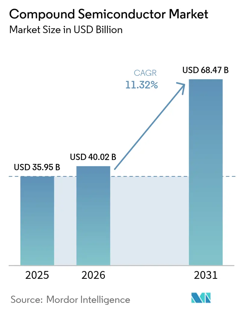
| Market Size (2026) | USD 40.02 Billion |
| Market Size (2031) | USD 68.47 Billion |
| Growth Rate (2026 - 2031) | 11.32% CAGR |
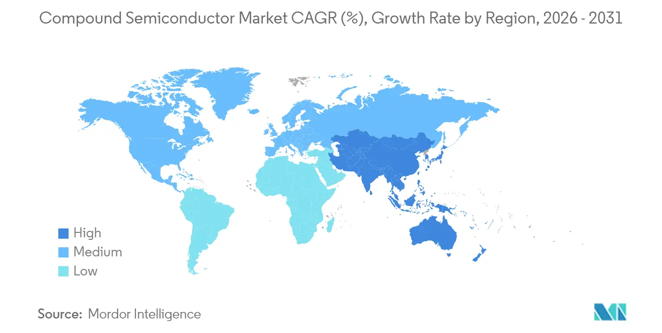
| Fastest Growing Market | Asia Pacific |
| Largest Market | Asia-Pacific |
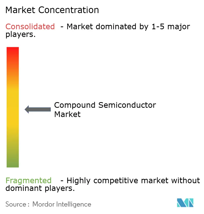
| Market Concentration | Medium |
Major Players *Disclaimer: Major Players sorted in no particular order Image © Mordor Intelligence. Reuse requires attribution under CC BY 4.0. | |
Compound Semiconductor Market Analysis by Mordor Intelligence
The compound semiconductor market size in 2026 is estimated at USD 40.02 billion, growing from 2025 value of USD 35.95 billion with 2031 projections showing USD 68.47 billion, growing at 11.32% CAGR over 2026-2031. Momentum came from the widening use of wide-bandgap materials that boosted efficiency in power electronics, RF communications, and optoelectronics. Rising electric vehicle charging infrastructure, accelerating 5G standalone deployments, and premium display demand collectively lifted unit shipments and average selling prices. Foundry capacity hikes in Asia-Pacific, domestic-manufacturing incentives in the United States and Europe, and sustained capital spending by automotive OEMs sustained the investment cycle. At the same time, geopolitical export controls on gallium, germanium, and indium, coupled with weather-related raw-material disruptions, highlighted supply-chain fragility and underscored the strategic value of diversified sourcing.
Key Report Takeaways
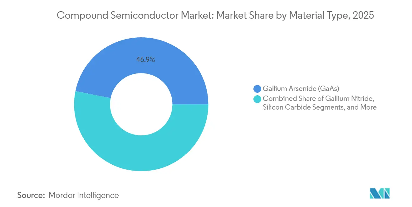
- By material type, gallium arsenide led with 46.85% revenue share in 2025, while silicon carbide is projected to expand at an 18.1% CAGR through 2031.
- By wafer size, the 150 mm category accounted for 48.02% of the compound semiconductor market share in 2025; 200 mm wafers are expected to grow at a 14.95% CAGR to 2031.
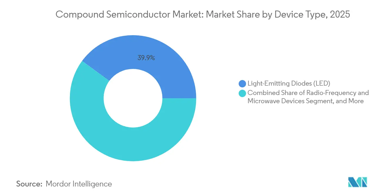
- By device type, LEDs captured 39.92% revenue in 2025, whereas power electronics are advancing at a 16.75% CAGR through 2031.
- By end-user industry, telecom and datacom infrastructure held 27.85% of the compound semiconductor market size in 2025, and automotive and transportation are forecast to grow at a 18.9% CAGR between 2026 and 2031.
- By geography, Asia-Pacific commanded 58.25% revenue in 2025; the region is on track for a 13.95% CAGR to 2031.
Note: Market size and forecast figures in this report are generated using Mordor Intelligence’s proprietary estimation framework, updated with the latest available data and insights as of 2026.
Global Compound Semiconductor Market Trends and Insights
Drivers Impact Analysis*
| Driver | (~) % Impact on CAGR Forecast | Geographic Relevance | Impact Timeline |
|---|---|---|---|
| GaN-on-Si power devices in EU and China EV chargers | +2.1% | Europe and China, spill-over to North America | Medium term (2-4 years) |
| 5G massive-MIMO RF front-ends in US and APAC | +1.8% | North America and APAC core, spill-over to Europe | Short term (≤ 2 years) |
| Micro/Mini-LED adoption in TVs and AR wearables | +1.4% | Global, early gains in APAC manufacturing hubs | Medium term (2-4 years) |
| SiC traction inverters for European commercial EVs | +1.9% | Europe's core, expanding to North America and China | Medium term (2-4 years) |
| III-V fab incentives under US/EU CHIPS Acts | +1.3% | North America and Europe, a competitive response in APAC | Long term (≥ 4 years) |
| InP-based LiDAR PICs for autonomous vehicles | +0.9% | Global, early deployment in developed markets | Long term (≥ 4 years) |
| Source: Mordor Intelligence | |||


GaN-on-Si power devices in EU and China EV chargers
European emissions rules and China’s highway electrification drove GaN-on-Si adoption in 350 kW and higher fast chargers that achieved 95% power-conversion efficiency and cut installation costs by up to 40% compared with silicon alternatives.[1]HAL Science, “Vertical GaN Devices: Reliability Challenges,” hal.science EU Green Deal funding of EUR 2 billion (USD 2.26 billion) for wide-bandgap fabs reinforced the transition, while China’s gallium export curbs spurred local sourcing strategies.
5G massive-MIMO RF front-ends in US and APAC
The migration toward standalone 5G and 64T64R or larger antenna arrays required GaAs and GaN power amplifiers that reduced base-station energy use by 40% and enabled millimeter-wave coverage. Initial deployments in South Korea reached 95% population coverage, and CHIPS Act grants prepared US fabs for domestic GaAs expansion.
Micro/Mini-LED adoption in TVs and AR wearables
Panel makers migrated from OLED to micro-LED for premium displays. Apple prototype smartphones integrated GaN-on-sapphire micro-LEDs that delivered 6,800 PPI and 50% lower power draw than OLED, while automotive cockpits adopted the tech for sunlight-readable dashboards.
SiC traction inverters for European commercial EVs
Mercedes-Benz eTruck platforms used SiC MOSFETs in 800 V inverters that reached 98% efficiency and reduced cooling complexity by 25%. Infineon’s EUR 7 billion (USD 7.91 billion) Malaysia fab targeted 30% of global SiC power capacity by 2030.
Restraints Impact Analysis*
| Restraint | (~) % Impact on CAGR Forecast | Geographic Relevance | Impact Timeline |
|---|---|---|---|
| Shortage of 200 mm SiC substrates | -1.7% | Global, acute impact in automotive chains | Short term (≤ 2 years) |
| High Cap-Ex of MOCVD reactors | -1.2% | Global, particularly for new entrants | Medium term (2-4 years) |
| Reliability concerns in >650 V GaN devices | -0.8% | Global, regulatory scrutiny in automotive | Medium term (2-4 years) |
| US export controls on epi tools to China | -0.9% | China's core, spillover globally | Long term (≥ 4 years) |
| Source: Mordor Intelligence | |||
Shortage of 200 mm SiC substrates
Manufacturers reported a 40% supply gap for 200 mm SiC wafers because boule growth cycles took up to 14 days, and furnace capacity was limited. Automotive OEMs, therefore, locked multi-year deals at premium prices, and substrate makers such as II-VI gained pricing power.
High Cap-Ex of MOCVD reactors
A single metal-organic chemical-vapor-deposition reactor costs USD 3-8 million, and a 200 mm GaN line demands as many as 15 units, raising entry barriers above USD 40 million. The dominance of two tool vendors constrained scaling and encouraged consolidation among smaller fabs.
*Our forecasts treat driver/restraint impacts as directional, not additive. The impact forecasts reflect baseline growth, mix effects, and variable interactions.
Segment Analysis
By Material Type: SiC Accelerates as GaAs Holds the Lead
The compound semiconductor market size for materials saw gallium arsenide retain a 46.85% share in 2025. Silicon carbide recorded an 18.1% CAGR outlook, underpinned by traction inverters and fast-charging power modules. Gallium nitride took incremental share through 650 V bidirectional IC launches that widened adoption in energy-storage bidirectional chargers. Indium phosphide remained essential in LiDAR photonic integrated circuits and sub-THz 6G prototypes, although absolute volumes were low.
Segment growth hinged on wide-bandgap attributes, high electron mobility and high breakdown voltage, that silicon could not match. Research breakthroughs in RF GaN-on-Si promised to extend GaN usage into 6G base-station PAs. Cost pressures lingered because gallium and indium feedstock remained under export-control scrutiny, raising interest in recycled sources and material alternatives such as AlYN.


By Wafer Size: 200 mm Drives Cost Optimisation
In 2025, 150 mm substrates captured 48.02% revenue, yet 200 mm platforms projected the fastest 14.95% CAGR. Automotive power modules, which depend on high die counts, favoured 200 mm to secure a projected 30% die-per-wafer cost saving over 150 mm lines. Infineon’s Malaysia megafab validated the scale economics with 200 mm SiC lines designed for 30% of global supply by 2030.
Smaller (≤ 100 mm) formats preserved positions in low-volume, performance-critical sectors such as satellite communications. While 300 mm opportunities emerged in GaN-on-Si prototypes, technical hurdles—film stress, bow control, and defect density—kept commercial adoption beyond the forecast period. Equipment suppliers prioritised 200 mm reactor platforms to maximise utilisation, targeting 85-90% loading to amortise capital costs.
By Device Type: Power Electronics Overtakes Traditional LEDs
LEDs accounted for 39.92% revenue in 2025, but power-electronics devices are forecast to post a 16.75% CAGR, pushing the compound semiconductor market toward electrification. Tesla’s SiC-based traction inverters set a benchmark, delivering a 5% range gain, which subsequently drove similar adoptions across commercial trucks and buses. RF and microwave devices expanded steadily as 5G and satellite backhaul demanded linear high-efficiency PAs.
Optoelectronics such as vertical-cavity surface-emitting lasers entered automotive LiDAR and high-speed optical interconnects, whereas photovoltaic cells stayed limited to space applications where gallium arsenide triple-junction architectures justified premium pricing. The rising power-device mix improved overall ASPs and margins for integrated device makers, thereby underpinning cap-ex allocation toward wide-bandgap fab expansions.
By End-User Industry: Automotive Transformation Shapes Demand
Telecom and datacom held 27.85% of the compound semiconductor market share in 2025, yet automotive is projected to expand at a 18.9% CAGR on the back of electrified drivetrains and advanced driver-assistance systems. BYD’s full-platform SiC integration yielded a 10% drivetrain-efficiency gain, validating value creation in even mid-range passenger models. Consumer electronics remained a stable, albeit slower-growing, contributor as flagship smartphones integrated GaAs/GaN RF front-ends and next-generation micro-LED displays.
Industrial and energy sectors leveraged SiC and GaN in solar inverters and utility-scale battery energy-storage systems to reduce conversion losses. Aerospace and defense continued to command high ASPs for radar and satellite payloads. Healthcare represented an emerging niche, with compound semiconductors powering wireless implants and precision diagnostic lasers.
Geography Analysis
Asia-Pacific held 58.25% revenue in 2025 and posted a 13.95% CAGR outlook to 2031. The compound semiconductor market size for the region benefited from China’s planned 8.6 million-wafer-per-month capacity and Taiwan’s foundry dominance. Export controls on gallium, germanium, and indium introduced in 2024 highlighted concentration risks, prompting local governments to channel subsidies toward upstream materials.
North America advanced domestic supply-chain agendas under the USD 39 billion CHIPS incentive. Skyworks and Qorvo lined up GaAs expansion projects, and TSMC’s USD 165 billion Arizona cluster accelerated to include compound-semiconductor advanced-packaging capability. Defense requirements for assured access to III-V devices added impetus.
Europe positioned wide-bandgap semiconductors as a pillar of its Green Deal and European Chips Act. Germany allocated EUR 2 billion (USD 2.26 billion) to local production, while Nexperia committed USD 200 million for a Hamburg SiC line. Supply-chain localisation aims to mitigate Asia-centric shocks such as the quartz-mine disruption in North Carolina that threatened 70-90% of global high-purity quartz.

Competitive Landscape
Industry concentration evolved toward moderate levels. Five vendors held more than 90% of the SiC power niche, yet diversified portfolios in RF and optoelectronics diluted overall dominance. STMicroelectronics led SiC power at 32.6% share, underpinned by a EUR 5 billion (USD 5.65 billion) Italian expansion. Infineon acquired GaN Systems and launched a USD 7.91 billion Malaysia fab. Onsemi purchased Qorvo’s SiC JFET line for USD 115 million, accelerating vertical integration.
Substrate technology and epitaxial process control remained key differentiators. Patent-portfolio races centred on vertical GaN structures and AlYN compounds.[4]Total Telecom, “Nexperia to Invest USD 200 Million in Hamburg,” totaltele.com Fabless challengers such as Transphorm targeted niche automotive power modules, leveraging outsourcing to lift asset efficiency. Government incentives shaped location decisions, with US and EU grants favouring domestic fabs for strategic autonomy.
Second-tier players focused on specialty markets—InP photonics, micro-LED epi wafers, and high-efficiency space solar cells—where performance outweighed scale. Strategic alliances between tool vendors and materials suppliers shortened process-qual cycles, enabling quicker customer qualifications and reinforcing incumbent positions.
Compound Semiconductor Industry Leaders
Skyworks Solutions Inc.
Wolfspeed Inc.
Qorvo Inc.
Analog Devices Inc.
OSRAM GmbH (ams-OSRAM AG)
- *Disclaimer: Major Players sorted in no particular order

Recent Industry Developments
- June 2025: TSMC advanced its USD 165 billion Arizona project schedule.
- June 2025: Imec achieved record RF GaN-on-Si efficiency for 6G PAs.
- April 2025: Taiwan substrate leaders reported double-digit revenue growth as AI server orders recovered.
- April 2025: Navitas released the first production 650V bidirectional GaNFast ICs.


Global Compound Semiconductor Market Report Scope
A semiconductor made of two or more elements is called a compound semiconductor, and the silicon of the semiconductor is made from a single element. The studied market is segmented by Type, such as Gallium Arsenide (GaAs), Gallium Nitride (GaN), Gallium Phosphide (GaP), Silicon Carbide (SiC)), Product (LED RF, Optoelectronics, and Power Electronics among various applications such as Telecommunications, Information & Communication Technology, Defense & Aerospace, Consumer Electronics, Healthcare, Automotive in multiple geographies. Further, the impact of macroeconomic trends on the Market is also covered under the scope of the study. Further, the disturbance of the factors affecting the Market's evolution in the near future has been covered in the study regarding drivers and constraints. The market sizes and predictions are provided in terms of value in USD for all the above segments.
| Gallium Arsenide (GaAs) |
| Gallium Nitride (GaN) |
| Silicon Carbide (SiC) |
| Indium Phosphide (InP) |
| Gallium Phosphide (GaP) |
| Other III-V and II-VI Compounds |
| ≤100 mm |
| 150 mm |
| 200 mm |
| 300 mm and Above |
| Light-Emitting Diodes (LED) |
| Radio-Frequency and Microwave Devices |
| Optoelectronics (Laser, Photodetector) |
| Power Electronics |
| Photovoltaic Cells |
| Telecom and Datacom Infrastructure |
| Consumer Electronics |
| Automotive and Transportation |
| Industrial and Energy |
| Aerospace and Defense |
| Healthcare and Life Sciences |
| Others |
| North America | United States | |
| Canada | ||
| Mexico | ||
| Europe | Germany | |
| United Kingdom | ||
| France | ||
| Italy | ||
| Nordics (Sweden, Finland, Norway, Denmark) | ||
| Rest of Europe | ||
| Asia-Pacific | China | |
| Japan | ||
| South Korea | ||
| India | ||
| Taiwan | ||
| Rest of Asia-Pacific | ||
| South America | Brazil | |
| Argentina | ||
| Mexico | ||
| Rest of South America | ||
| Middle East and Africa | Middle East | Saudi Arabia |
| United Arab Emirates | ||
| Turkey | ||
| Rest of Middle East | ||
| Africa | South Africa | |
| Rest of Africa | ||
| By Material Type | Gallium Arsenide (GaAs) | ||
| Gallium Nitride (GaN) | |||
| Silicon Carbide (SiC) | |||
| Indium Phosphide (InP) | |||
| Gallium Phosphide (GaP) | |||
| Other III-V and II-VI Compounds | |||
| By Wafer Size | ≤100 mm | ||
| 150 mm | |||
| 200 mm | |||
| 300 mm and Above | |||
| By Device Type | Light-Emitting Diodes (LED) | ||
| Radio-Frequency and Microwave Devices | |||
| Optoelectronics (Laser, Photodetector) | |||
| Power Electronics | |||
| Photovoltaic Cells | |||
| By End-User Industry | Telecom and Datacom Infrastructure | ||
| Consumer Electronics | |||
| Automotive and Transportation | |||
| Industrial and Energy | |||
| Aerospace and Defense | |||
| Healthcare and Life Sciences | |||
| Others | |||
| By Geography | North America | United States | |
| Canada | |||
| Mexico | |||
| Europe | Germany | ||
| United Kingdom | |||
| France | |||
| Italy | |||
| Nordics (Sweden, Finland, Norway, Denmark) | |||
| Rest of Europe | |||
| Asia-Pacific | China | ||
| Japan | |||
| South Korea | |||
| India | |||
| Taiwan | |||
| Rest of Asia-Pacific | |||
| South America | Brazil | ||
| Argentina | |||
| Mexico | |||
| Rest of South America | |||
| Middle East and Africa | Middle East | Saudi Arabia | |
| United Arab Emirates | |||
| Turkey | |||
| Rest of Middle East | |||
| Africa | South Africa | ||
| Rest of Africa | |||


Key Questions Answered in the Report
What is the current value of the compound semiconductor market?
The compound semiconductor market was valued at USD 40.02 billion in 2026.
How fast is the compound semiconductor market expected to grow?
The market is projected to grow at a 11.32% CAGR, reaching USD 68.47 billion by 2031.
Which region leads the compound semiconductor market?
Asia-Pacific held 58.25% revenue in 2025, driven by large-scale manufacturing capacity.
Why are 200 mm SiC wafers important?
They lower die cost by roughly 30% versus 150 mm wafers, which supports automotive electrification.
Who dominates the SiC power-device segment?
STMicroelectronics led with 32.6% share, and the top five companies controlled more than 90% of the niche.
What is the main growth driver for compound semiconductor demand in automotive?
SiC traction inverters and GaN fast chargers improve efficiency and support higher-voltage EV architectures.
Page last updated on:


