Technology, Media and Telecom
5th MayPricing Strategy for Semiconductor Components
3 Min Read
Semiconductor Materials Market Segmented by Application (Fabrication, Packaging), Material Type (Wafer Substrates, Specialty and More), End-User Industry (Consumer Electronics, Telecommunications, and More), Technology Node, Fab Ownership (IDM, Pure-Play and More), and Geography. The Market Forecasts are Provided in Terms of Value (USD).
Market Overview
| Study Period | 2019 - 2030 |
|---|---|
| Market Size (2025) | USD 80.79 Billion |
| Market Size (2030) | USD 101.89 Billion |
| Growth Rate (2025 - 2030) | 4.75 % CAGR |
| Fastest Growing Market | North America |
| Largest Market | Asia Pacific |
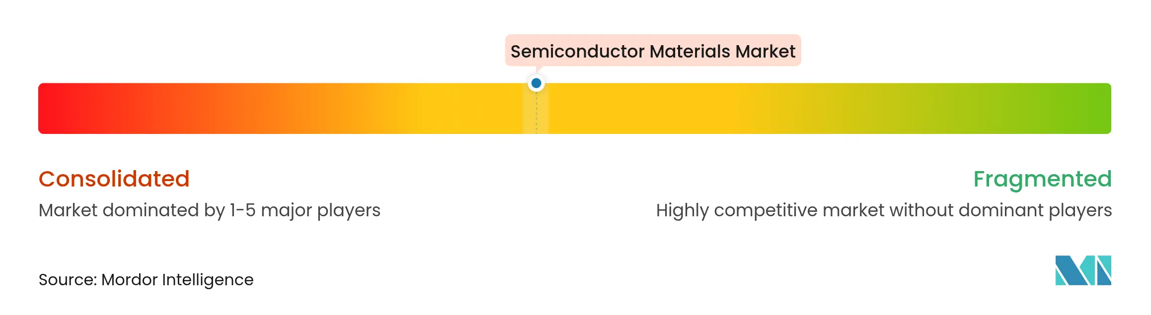
| Market Concentration | Medium |
Major Players*Disclaimer: Major Players sorted in no particular order. Image © Mordor Intelligence. Reuse requires attribution under CC BY 4.0. |
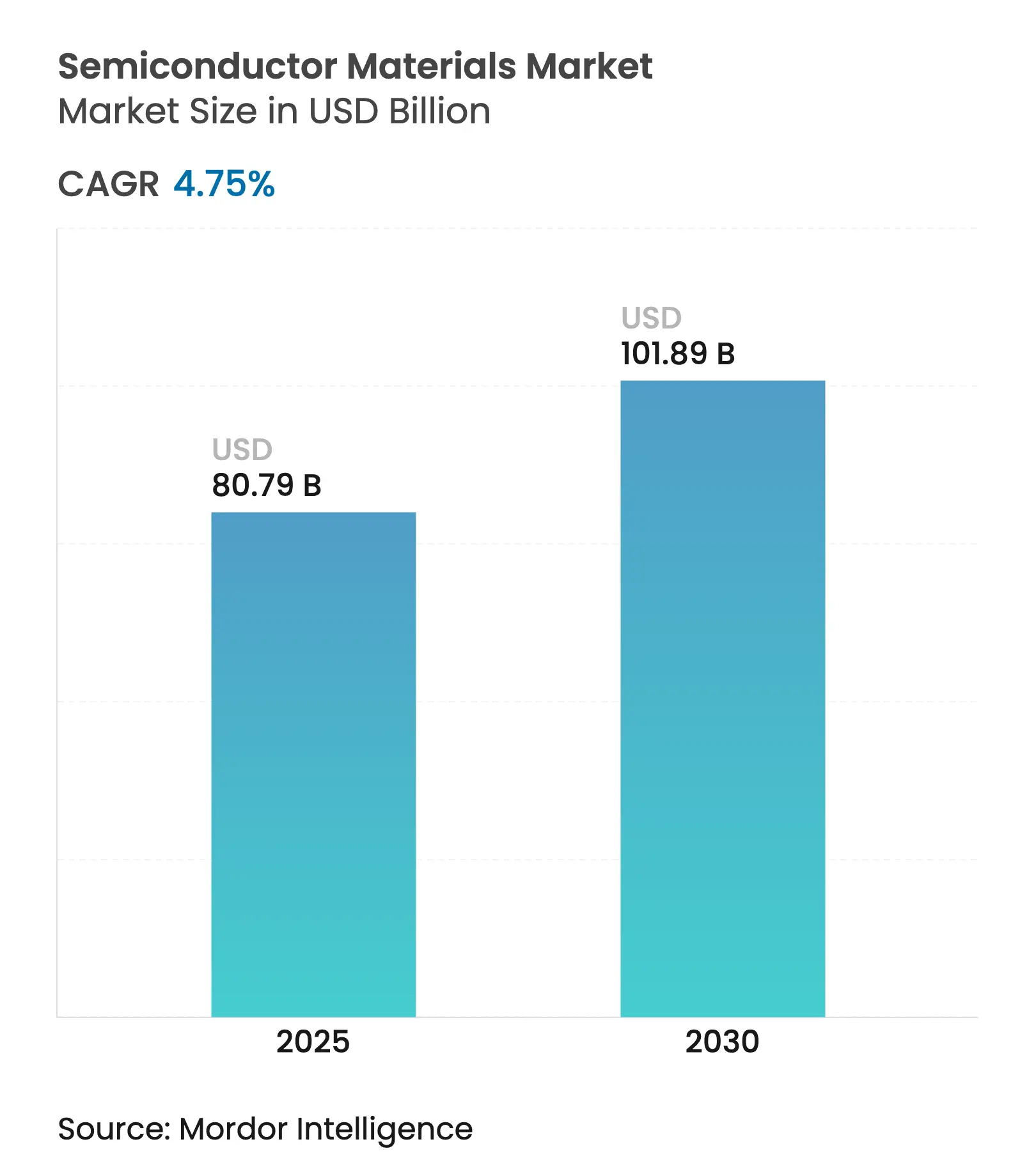
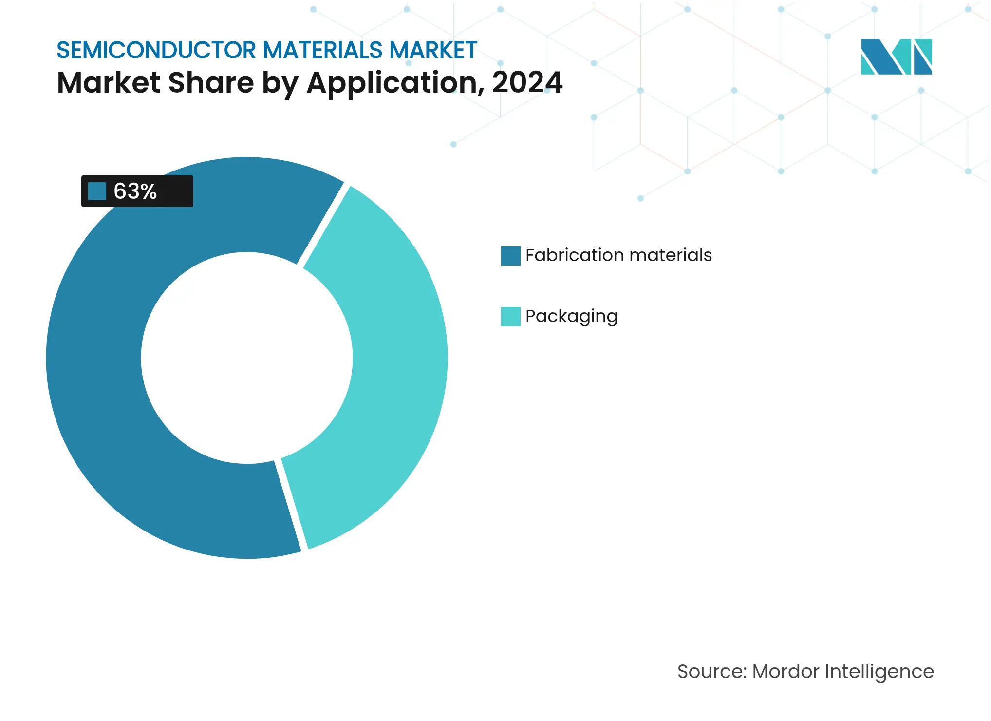
The semiconductor materials market size reached USD 80.79 billion in 2025 and is projected to expand to USD 101.89 billion by 2030, advancing at a 4.75% CAGR during the forecast period. Continued AI-optimized architectures and automotive electrification are reshaping material requirements as traditional silicon approaches fundamental physics limits. Advanced packaging materials are accelerating at an 11.8% CAGR because chiplet designs and 3D stacking architectures need novel interconnect and thermal solutions. Fabrication materials still dominate with a 63% revenue share in 2024, but value creation is migrating downstream where packaging innovation increasingly shapes system performance. Demand is also buoyed by the pivot to wide-bandgap power devices in electric vehicles and by strategic reshoring programs that incentivize domestic material supply chains in North America and Europe. Geopolitical tensions surrounding critical chemicals—most visibly Japan’s 2019 hydrogen-fluoride curbs—have underscored the importance of diversified sourcing strategies. [1]Source: Semi Staff, “Global Semiconductor Packaging Material Market Outlook Shows Return to Growth Starting in 2024,” SEMI, semi.org
Key Report Takeaways
Drivers Impact Analysis
| Driver | (~) % Impact on CAGR Forecast | Geographic Relevance | Impact Timeline | |||
|---|---|---|---|---|---|---|
Digitalization-led fab expansions Digitalization-led fab expansions | 1.20% | Global, with concentration in APAC and North America | Medium term (2-4 years) | (~) % Impact on CAGR Forecast:1.20% | Geographic Relevance:Global, with concentration in APAC and North America | Impact Timeline:Medium term (2-4 years) |
5G/AI end-device proliferation 5G/AI end-device proliferation | 0.80% | Global, led by North America and China | Short term (≤ 2 years) | |||
Automotive electrification & ADAS Automotive electrification & ADAS | 0.60% | Global, with early adoption in Europe and China | Medium term (2-4 years) | |||
Advanced-node investments (≤5 nm) Advanced-node investments (≤5 nm) | 0.50% | APAC core, with expansion to North America | Long term (≥ 4 years) | |||
Chiplet & heterogenous integration BOM uplift Chiplet & heterogenous integration BOM uplift | 0.40% | Global, concentrated in high-performance computing hubs | Medium term (2-4 years) | |||
Regionalisation-driven safety-stock policies Regionalisation-driven safety-stock policies | 0.30% | North America and Europe primarily | Short term (≤ 2 years) | |||
| Source: Mordor Intelligence | ||||||
Digitalization-led Fab Expansions
The USD 400 billion earmarked for 300 mm fab equipment through 2027 represents the largest capacity build-out in semiconductor history. Texas Instruments alone has committed USD 60 billion across seven US fabs, while Micron plans USD 200 billion in domestic memory facilities. . Each advanced fab consumes 40% more specialty chemicals per wafer than the previous generation, intensifying pressure on suppliers to scale ultra-high-purity production in multiple geographies.[2]Applied Materials Press Team, “Global Semiconductor Industry Planning USD 400 Billion Investment in 300 mm Fab Equipment (2025-2027),” Applied Materials, appliedmaterials.com
5G/AI End-Device Proliferation
AI accelerators push unprecedented bandwidth and thermal envelopes, tripling materials spend per packaged chip relative to conventional processors. HBM stacks rely on through-silicon-via copper pillars and ultra-thin die-attach films that demand silver-rich formulations. Fujifilm has targeted JPY 500 billion in semiconductor-materials revenue by 2030, largely from EUV photoresists tailored for AI-centric nodes. On the automotive side, LG Chem’s high-performance silver paste for SiC power modules exemplifies how AI-driven mobility raises both temperature and voltage requirements.
Automotive Electrification & ADAS
SiC demand is growing at a 20% CAGR and could reach USD 11-14 billion by 2030 as electric drivetrains shift to 800 V architectures that exceed silicon’s thermal limits. Infineon plans 12-inch GaN sample rollout by 4Q 2025 to lower cost per device and accelerate traction-inverter adoption. China’s recent gallium export restrictions underscore raw-material risks for GaN devices, prompting OEMs to localize supply and investigate alternative chemistries. Auto-grade qualification cycles run up to three years, reinforcing sticky, premium material demand once designed-in.
Advanced-Node Investments (≤5 nm)
Intel’s 2 nm milestone highlights the atomic-level precision now required for high-NA EUV resists, dry-clean etchants and selective-deposition precursors. EUV transitions have already cut PFAS use per wafer by 18%, accelerating the search for non-PFAS chemistries. Glass core substrates under joint development by Intel, AMD and Samsung aim to replace organic laminates between 2025-2026, improving coefficient-of-thermal-expansion matching for ultra-large reticle-scale packages.
Restraints Impact Analysis
| Restraint | (~) % Impact on CAGR Forecast | Geographic Relevance | Impact Timeline | |||
|---|---|---|---|---|---|---|
Cyclicality of consumer electronics Cyclicality of consumer electronics | -0.90% | Global, with highest impact in APAC manufacturing hubs | Short term (≤ 2 years) | (~) % Impact on CAGR Forecast:-0.90% | Geographic Relevance:Global, with highest impact in APAC manufacturing hubs | Impact Timeline:Short term (≤ 2 years) |
High capital intensity for new chemistries High capital intensity for new chemistries | -0.70% | Global, affecting all regions with semiconductor manufacturing | Medium term (2-4 years) | |||
Environmental regulations on PFAS chemistries Environmental regulations on PFAS chemistries | -0.40% | Europe and North America primarily, spreading globally | Long term (≥ 4 years) | |||
Hydrogen fluoride supply security in APAC Hydrogen fluoride supply security in APAC | -0.30% | APAC core, with spillover effects globally | Medium term (2-4 years) | |||
| Source: Mordor Intelligence | ||||||
Cyclicality of Consumer Electronics
The semiconductor packaging materials segment fell 15.5% in 2023 before rebounding in 2024, illustrating how smartphone and PC slowdowns ripple quickly through chemical demand. Inventory swings of up to 30% within a quarter pressure suppliers devoted to high-volume consumer lines. Diversification into automotive, industrial and infrastructure is mitigating but not eliminating this volatility. The advent of AI-enhanced consumer devices may lower cyclical amplitude yet introduce fresh forecasting complexity as bill-of-materials inflation replaces unit growth as the primary revenue lever.
High Capital Intensity for New Chemistries
Each next-generation formulation demands USD 50-100 million in pilot and scale-up investment, with a three-to-five-year qualification window. BASF’s EUR 100 million sulfuric-acid upgrade in Germany typifies the outlay needed to meet 1-part-per-trillion purity specs. Parallel production of legacy and replacement materials during qualification phases locks up working capital and favours deep-pocketed incumbents. The voluntary PFOA phase-out announced by the Semiconductor Industry Association in July 2024 further complicates cost recovery for PFAS-free alternatives.
By Application: Fabrication Dominance Drives Market Scale
Fabrication materials commanded 63% revenue in 2024, reflecting the hundreds of etch, deposition and planarization steps per wafer. Wet chemicals, electronic gases and CMP consumables form the largest cost pools. In value terms, this slice of the semiconductor materials market size equated to more than USD 50 billion in 2024. Advanced packaging, while smaller today, is scaling at a 9.2% CAGR as chiplet partitioning pushes metallization density and thermal-interface performance beyond organic laminate capabilities. The semiconductor materials market is therefore tilting toward substrates, under-fills and mold compounds engineered for multi-die architectures, supported by an 11.8% CAGR in packaging raw materials.
The pivot also recasts industry power dynamics. Fabrication suppliers benefit from scale but face flatter growth curves, whereas packaging innovators can secure design-in wins with higher long-term elasticity. For instance, BT-resin-based substrates enable finer lines and spaces than traditional FR-4, unlocking performance gains in AI accelerators. Materials vendors that straddle both process nodes and package architectures gain cross-cycle resilience, capturing spend both at wafer start and at module finish.
By Material Type: Wet Chemicals Lead Traditional Segments
Wet-process chemicals remained the largest material class, representing 24% of 2024 spend, thanks to their universal role in cleaning, stripping and etching. Ongoing node migration increases dosage intensity—leading-edge fabs use 40% more acids and bases per wafer than 28 nm lines. Specialty gases, including hydrogen fluoride and nitrogen trifluoride, follow closely in value and face geopolitical supply scrutiny. Japan’s 2019 export restrictions slashed hydrogen-fluoride shipments to South Korea by 96.8%, prompting rapid dual-sourcing across Taiwan, Belgium and the United States.
CMP slurries and pads show steady upticks as the number of planarization steps rises with each design shrink. Photoresists evolve with EUV adoption; new polymer platforms must endure 13.5 nm photon bombardment without line-edge roughness degradation. Substrate innovation is broadening beyond 300 mm silicon to include high-quality SiC boules and 200 mm GaN wafers for power devices. Collectively, these shifts are reshaping the semiconductor materials market, forcing suppliers to balance purity, sustainability and cost.
By End-User Industry: Consumer Electronics Dominance Challenged
Consumer electronics still accounted for 38% of 2024 revenue, yet growth is plateauing as shipment volumes stabilize. Conversely, automotive demand is rising at an 8.7% CAGR. Electric vehicles integrate 3,000 semiconductor devices—double that of internal-combustion cars—amplifying package counts and die sizes. As a result, automotive orders are increasingly dictating allocations for SiC substrates, high-temperature die-attach alloys and advanced encapsulants.
Telecommunications infrastructure also supports demand through 5G base-station deployments that consume RF front-end gallium arsenide and power-amplifier-grade GaN. Industrial IoT and energy grid modernization add another layer of steady pull for high-reliability semiconductors, broadening the semiconductor materials market beyond cyclical consumer refresh cycles.

Recognized by Experts. Trusted by Leaders.
A trusted intelligence partner to global decision-makers across 90+ countries.


By Technology Node: Mature Processes Retain Scale Advantage
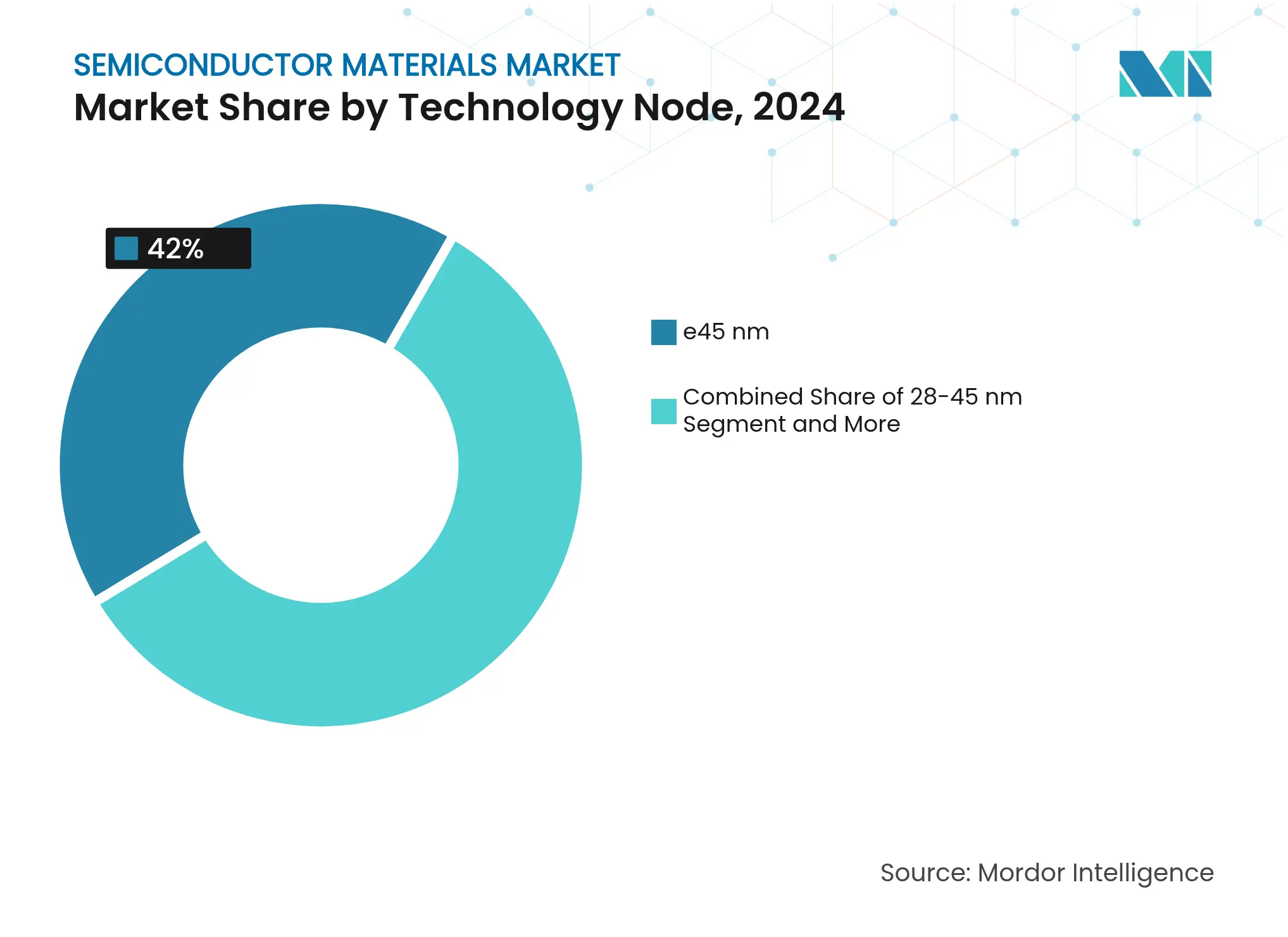
Nodes ≥45 nm retained 42% market share in 2024 because analog, power and automotive microcontrollers value cost and reliability. That scale anchors baseline chemical demand for legacy fabs worldwide. Meanwhile, ≤5 nm processes are advancing at a 14.5% CAGR, fuelled by AI accelerators and flagship smartphone SoCs. Here, the semiconductor materials market size per wafer is two to three times greater than in mature nodes due to multi-patterning, PEALD liners and high-NA EUV photoresists.
Mid-nodes at 14–22 nm offer balanced cost-performance for high-volume applications, while 28–45 nm remains a sweet spot for price-sensitive automotive controllers. Japan’s USD 30 billion stimulus to sustain domestic capacity across all nodes signals policymaker recognition that resilience extends beyond the bleeding edge.
Note: Segment shares of all individual segments available upon report purchase
By Fab Ownership: IDM Model Maintains Materials Advantage
IDMs captured 41% of 2024 revenue because vertical integration lets them co-optimize materials and design. Intel’s internal glass-core substrate program exemplifies how IDMs use proprietary supply chains to differentiate. Pure-play foundries are growing faster-10.3% CAGR-by aggregating fabless demand, compelling suppliers to qualify materials across wider process portfolios. Fabless firms influence chemistry choices indirectly via design-kit specifications, while OSATs drive specialty packaging materials such as wafer-level under-fills and mold compounds. The semiconductor materials market therefore remains shaped by a tri-polar procurement model spanning captive, foundry and outsourced assembly customers.
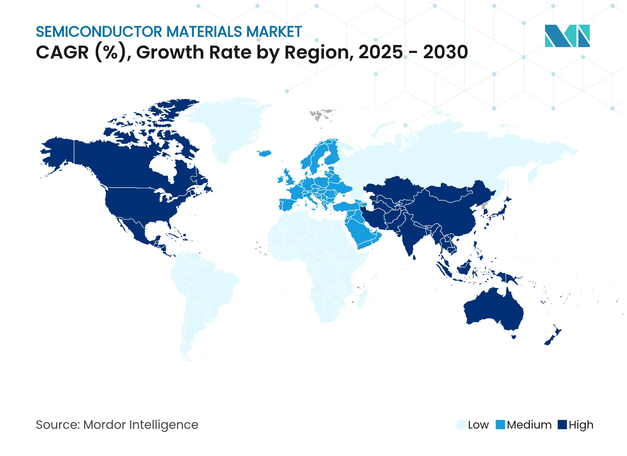
Asia-Pacific commanded 55% of 2024 revenue owing to its dense manufacturing ecosystem across Taiwan, South Korea, Japan and mainland China. However, the region’s concentration exposes supply chains to export-control shocks as evidenced by the 2019 hydrogen-fluoride episode. Japanese suppliers are fortifying resilience with USD 545 million in new chemical plants and targeted acquisitions to secure local control of high-purity lines.
North America is the fastest-growing territory, advancing at a 6.4% CAGR through 2030 on the back of USD 52 billion in CHIPS Act incentives. Intel, TSMC and Samsung are collectively building more than 20 million wafers per-year of capacity, catalysing parallel investments from Air Liquide (USD 250 million in Idaho) and Entegris (USD 75 million for Colorado Springs). Domestic packaging and test expansions are shortening lead times and stimulating demand for solder-ball alloys and advanced substrates produced within the region. Environmental regulators are simultaneously accelerating adoption of PFAS-free chemistries, giving local innovators a foothold.
Europe is leveraging its Chips Act to reach 20% global share by 2030. Merck, BASF and Linde are upgrading ultra-purity sulfuric and ammonia lines to support new fabs in Germany and France. India is emerging as a secondary hub for mature-node and OSAT work, attracting specialty-gas makers with greenfield investments. The Middle East and Africa remain nascent but could benefit from sovereign efforts to localize power-device assembly tied to renewable energy projects. Collectively these moves are geographically redistributing the semiconductor materials market, increasing total spend through redundancy while easing geopolitical risk. [3]Air Liquide Newsroom, “USD 250 Million Investment in Idaho to Support Micron,” Air Liquide, airliquide.com

Reports are available across multiple geographies.
Gain in-depth market insights across regions to support informed decisions.
Market Concentration
The market remains highly concentrated: five producers control more than four-fifths of global photoresist volume, and Japanese firms dominate high-purity hydrogen fluoride with over 90% share. DuPont, BASF and Shin-Etsu leverage decades of process know-how and secure long-term supply agreements that embed their chemistries deep into device qualifications. Capital-intensive expansions continue—Shin-Etsu is committing USD 545 million to new wet-chemical capacity, while BASF upgrades sulfuric-acid purity to sub-ppt levels.
Technology-driven partnerships are multiplying. Applied Materials bought a 9% stake in BE Semiconductor to co-develop hybrid-bonding consumables, while JSR fully acquired Yamanaka Hutech to gain precursor competency for atomic-layer deposition. Environmental regulation is a second competitive lever: the SIA’s voluntary PFOA phase-out is pushing incumbent fluorochemical houses to re-tool, opening windows for start-ups with PFAS-free surfactants.
Geographic diversification adds yet another dimension. Kyocera is pouring JPY 68 billion into Nagasaki ceramic-package lines and spinning up a USD 60 million venture fund to scout allied materials startups across the United States and EMEA. Companies able to synchronize regional capacity with customer fabs will capture incremental share as OEMs de-risk single-source dependencies. Overall, the semiconductor materials market is tilting toward a barbell structure that pairs deep-pocket incumbents with agile niche innovators. [4]BASF Corporate Communications, “BASF Investing in Semiconductor-Grade Sulfuric Acid Plant,” BASF, basf.com

*Disclaimer: Major Players sorted in no particular order
1. INTRODUCTION
2. RESEARCH METHODOLOGY
3. EXECUTIVE SUMMARY
4. MARKET LANDSCAPE
5. MARKET SIZE AND GROWTH FORECASTS (VALUE)
6. COMPETITIVE LANDSCAPE
7. MARKET OPPORTUNITIES AND FUTURE OUTLOOK
Semiconductors are silicon-based materials that conduct electricity better than insulators like glass, but they are not pure conductors like copper or aluminum. Materials used to pattern the wafer are considered fabrication materials for the scope of the study. In contrast, the materials used to protect or connect the die are called packing materials. Semiconductor fabrication is a set of operations that involves depositing a sequence of layers onto a substrate, most often silicon, to create a device structure. Various thin film layers are deposited and removed in this process. Photolithography regulates the portions of the thin film that are to be deposited or withdrawn. Cleaning and inspection stages are usually performed after each deposition and removal operation.
The semiconductor materials market is segmented by application (fabrication (process chemicals, photomasks, electronic gases, photoresists ancillaries, sputtering targets, silicon, and other fabrication materials) and packaging (substrates, lead frames, ceramic packages, bonding wire, encapsulation resins (liquid), die attach materials, and other packaging applications), end-user industry (consumer electronics, telecommunication, manufacturing, automotive, energy and utility, and other end-user industries), and geography (Taiwan, South Korea, China, Japan, North America, Europe, and Rest of the World). The market sizes and forecasts are provided in terms of value (USD) for all the above segments.
Pricing Strategy for Semiconductor Components
3 Min Read
Accelerating Additive Manufacturing Adoption in India
3 Min Read
When decisions matter, industry leaders turn to our analysts. Let’s talk.