Semiconductor Foundry Market Size and Share
Market Overview
| Study Period | 2020 - 2031 |
|---|---|
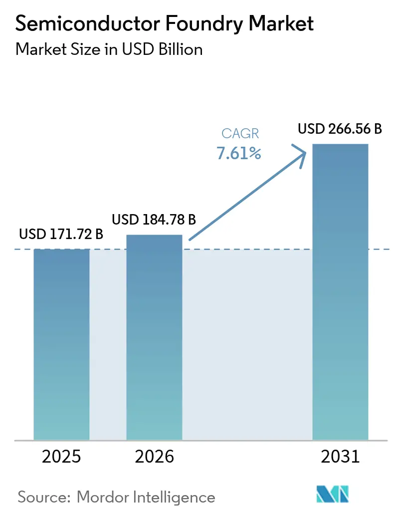
| Market Size (2026) | USD 184.78 Billion |
| Market Size (2031) | USD 266.56 Billion |
| Growth Rate (2026 - 2031) | 7.61% CAGR |
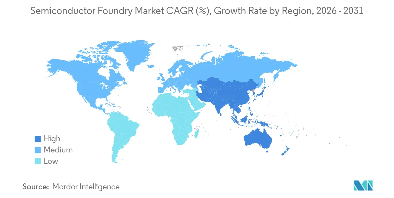
| Fastest Growing Market | Asia Pacific |
| Largest Market | Asia Pacific |
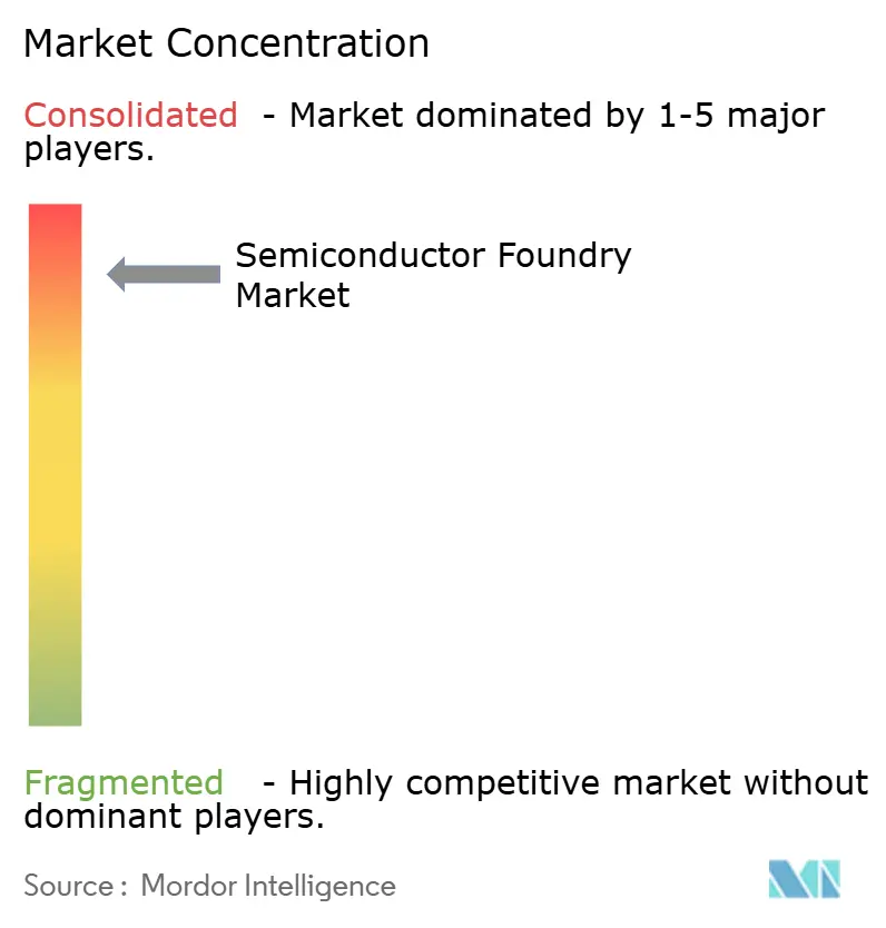
| Market Concentration | High |
Major Players
*Disclaimer: Major Players sorted in no particular order Image © Mordor Intelligence. Reuse requires attribution under CC BY 4.0. |
|
Semiconductor Foundry Market Analysis by Mordor Intelligence
The global semiconductor foundry market size in 2026 is estimated at USD 184.78 billion, growing from 2025 value of USD 171.72 billion with 2031 projections showing USD 266.56 billion, growing at 7.61% CAGR over 2026-2031. A combination of soaring artificial-intelligence compute needs at sub-5 nm, sustained demand for mature-node automotive chips, and intensive government incentives is widening both the technology and geographic footprint of the sector. Advanced packaging, especially chiplets and 3-D ICs, has become a parallel revenue engine, while water stewardship, export-control compliance, and EUV-tool talent shortages temper near-term capacity additions. Intensifying geopolitical competition is prompting North America, Europe, and India to localize fabrication, gradually diffusing Asia-Pacific’s traditional production dominance without dislodging its leadership. Competitive dynamics now hinge on node leadership below 5 nm, cost-efficient 28 nm capacity, and foundry-as-a-service offerings targeting start-ups.
Key Report Takeaways
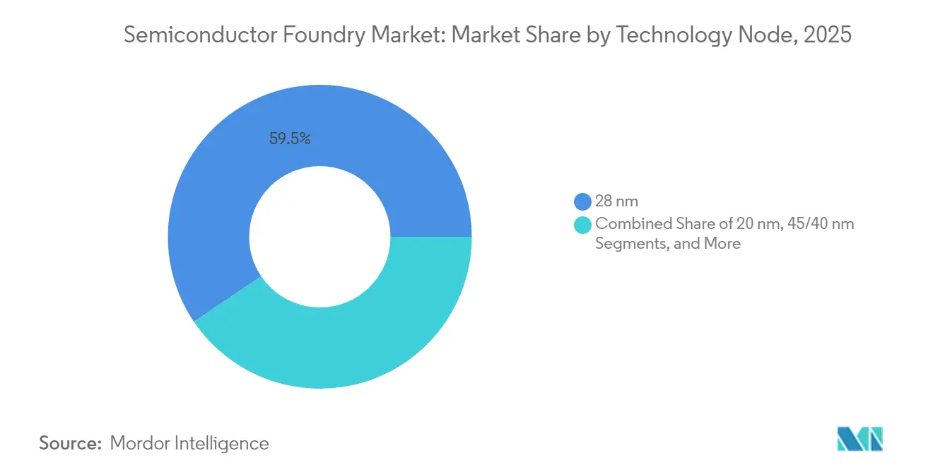
- By technology node, the 28 nm segment led with 59.45% of semiconductor foundry market share in 2025; nodes below 10 nm are expanding at a 9.05% CAGR through 2031.
- By wafer size, 300 mm substrates commanded 68.10% of the semiconductor foundry market size in 2025 and are growing at 9.42% CAGR to 2031.
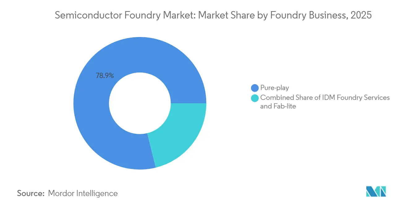
- By business model, pure-play foundries controlled 78.85% of semiconductor foundry market revenue in 2025, while IDM foundry services are the fastest-growing segment at a CAGR of 8.72%.
- By application, consumer electronics generated 70.95% of semiconductor foundry market demand in 2025, while automotive chips are advancing at a CAGR of 8.55% through 2031.
- By geography, Asia-Pacific held 22.65% of semiconductor foundry market revenue in 2025 and is projected to record the fastest regional expansion at a CAGR of 8.44% through 2031.
Note: Market size and forecast figures in this report are generated using Mordor Intelligence’s proprietary estimation framework, updated with the latest available data and insights as of 2026.
Global Semiconductor Foundry Market Trends and Insights
Drivers Impact Analysis*
| Driver | (~)% Impact on CAGR Forecast | Geographic Relevance | Impact Timeline |
|---|---|---|---|
| Mainstream chip demand from automotive electrification | +1.8% | Global, with concentration in Germany, Japan, China | Medium term (2-4 years) |
| IoT-edge proliferation requiring mature‐node capacity | +1.2% | APAC core, spill-over to North America | Short term (≤ 2 years) |
| AI accelerator race for <5 nm advanced nodes | +0.9% | Taiwan, South Korea, with expansion to US | Long term (≥ 4 years) |
| Chiplets + 3D IC needing new foundry workflows | +0.7% | Global, led by Taiwan and US innovation hubs | Medium term (2-4 years) |
| Defense agencies' push for trusted domestic fabs | +0.6% | US, EU, with emerging initiatives in India | Long term (≥ 4 years) |
| Foundry-as-a-Service model for start-ups | +0.5% | Silicon Valley, with expansion to global tech hubs | Short term (≤ 2 years) |
| Source: Mordor Intelligence | |||


AI Accelerator Race for Less than 5 nm Advanced Nodes
Sub-5 nm capacity has moved from niche to mainstream in the semiconductor foundry market as hyperscalers and chip designers race to train larger AI models. TSMC reported that 7 nm and finer nodes contributed 74% of wafer revenue in Q2 2025, underscoring the premium customers place on density leadership[1]Taiwan Semiconductor Manufacturing Company Limited, “TSMC Reports Second Quarter EPS of NTD 15.36,” pr.tsmc.com. Samsung’s gate-all-around 2 nm program and Intel’s 1.4 nm roadmap confirm an industry-wide pivot toward atomic-scale geometries. Rapid node migration is also fueling demand for advanced interposers, necessitating co-optimized fab and packaging lines. High capital intensity—often above USD 20 billion per fab—limits viable competitors and cements an oligopolistic market where process leadership directly dictates share.
Mainstream Chip Demand from Automotive Electrification
Electric vehicles are driving demand in the semiconductor foundry market, requiring dual-track silicon: power-management ICs at mature nodes and high-compute SoCs at leading nodes. Automakers’ shift to centralized electronic architectures locks in long-term 28 nm and 45 nm volumes, providing reliable backfill for fabs otherwise pressured by cyclical smartphone orders. Long qualification cycles and strict AEC-Q100 standards encourage multi-year capacity reservations, improving revenue visibility for foundries that balance mature and advanced nodes. Tesla’s custom chip strategy illustrates how OEMs use dedicated capacity deals to secure supply and differentiate performance.
Defense Agencies’ Push for Trusted Domestic Fabs
National security policy now ranks alongside cost in fab-site decisions. The U.S. CHIPS Act deployed USD 52.7 billion to reshore critical nodes, while the Department of Commerce funded a USD 285 million digital-twin institute to streamline domestic manufacturing scale-up [2]National Institute of Standards and Technology, “CHIPS Manufacturing USA Institute,” nist.gov . Europe’s Chips Act and India’s semiconductor mission mirror the model, collectively tilting new capacity announcements toward allied regions. Defense contracts guarantee baseline volumes and impose stringent provenance requirements, favoring foundries with secure, on-shore tool chains.
Chiplets + 3-D IC Needing New Foundry Workflows
Vertical stacking and chip-partitioning let designers mix DRAM, analog, RF, and logic dies for system-level gains that raw scaling can no longer provide. TSMC’s SoIC and Samsung’s X-Cube platforms pull packaging into the critical-path schedule, expanding the traditional foundry revenue envelope. New thermal budgets, TSV design rules, and test regimes create steep learning curves, further differentiating incumbents from latecomers. Average selling prices rise with package complexity, cushioning gross margins against cyclical swings in commodity logic demand.
Restraints Impact Analysis*
| Restraint | (~)% Impact on CAGR Forecast | Geographic Relevance | Impact Timeline |
|---|---|---|---|
| Geopolitical export-control uncertainty | -1.1% | Global, with acute impact on China-US trade | Short term (≤ 2 years) |
| Capex inflation and long pay-back periods | -0.8% | Global, with higher impact in high-cost regions | Medium term (2-4 years) |
| Water-use permits limiting mega-fabs | -0.6% | Water-stressed regions: Taiwan, Arizona, Texas | Long term (≥ 4 years) |
| Talent crunch in sub-3nm EUV maintenance | -0.4% | Advanced foundry locations: Taiwan, Korea, US | Medium term (2-4 years) |
| Source: Mordor Intelligence | |||
Geopolitical Export-Control Uncertainty
Expanded Foreign-Produced Direct Product rules restrict advanced lithography exports to specific countries, forcing fabs to segregate legacy and cutting-edge lines[3]Bureau of Industry and Security, “Foreign-Produced Direct Product Rule Additions,” federalregister.gov. Compliance costs rise as companies duplicate equipment sets and audits across jurisdictions. Malaysia’s tighter chip policies under U.S. pressure show knock-on effects in Southeast Asia, where routing high-end GPUs now triggers lengthy license reviews. Unpredictable rule-making discourages green-field projects, particularly at 5 nm and below, muting near-term investment cycles.
Talent Crunch in Sub-3 nm EUV Maintenance
Each EUV scanner contains more than 100,000 parts and demands hourly calibration to hit yield targets. With ASML the sole supplier and only a handful of universities teaching EUV optics, maintenance engineers command outsized premiums. Rapid fab expansion has outstripped the training pipeline, leaving some new lines underutilized while crews are certified. Unscheduled EUV downtime immediately erodes fab utilization and profit margins, making workforce development as critical as capex in sub-3 nm planning.
*Our forecasts treat driver/restraint impacts as directional, not additive. The impact forecasts reflect baseline growth, mix effects, and variable interactions.
Segment Analysis
By Technology Node: Advanced Nodes Capture Premium Growth
In 2025, the 28 nm node generated 59.45% revenue, anchoring the semiconductor foundry market size for cost-sensitive, high-volume devices. Nodes finer than 10 nm, although smaller in shipment volume, will produce a 9.05% CAGR through 2031, reflecting AI and HPC pull-through. Revenue mix therefore bifurcates: mature nodes assure predictable automotive and industrial cash flows, while leading-edge nodes command premium pricing and margins.
Capex discipline remains pivotal. TSMC begins 2 nm risk production in 2025, drawing prepayments from smartphone and accelerator clients. Intel and Samsung respond with 1.4 nm and 2 nm gate-all-around timelines, intensifying capital races. Meanwhile, 16 nm and 14 nm nodes bridge cost-performance gaps for networking silicon. Legacy 65 nm and above still serve analog and RF designs with long lifecycles, keeping fabs running at healthy utilization even when handset demand softens.


By Wafer Size: 300 mm Production Drives Cost Leadership
The transition to 300 mm tooling lifted die output per run and cut edge-loss waste, enabling the segment to capture 68.10% of the semiconductor foundry market share in 2025. Growth persists at 9.42% CAGR as new fabs select 300 mm equipment by default for anything below 40 nm. In contrast, 200 mm remains entrenched in MEMS, power GaN, and niche analog where geometry or chemistry complicates 300 mm migration.
Economies of scale are stark. A 300 mm fab reaching 100,000 wafers-per-month can undercut 200 mm cost per die by 30% once fully depreciated. Yet the USD 15–20 billion entry fee restricts newcomers, reinforcing incumbent advantage. Specialized 150 mm lines persist for SiC, GaAs, and photonics products that rely on exotic substrates.
By Foundry Business Model: Pure-Play Dominance Under IDM Challenge
Pure-play specialists such as TSMC, UMC, and GlobalFoundries booked 78.85% of 2025 revenue in the semiconductor foundry market, monetizing design enablement, process portability, and time-to-yield strengths. However, IDM foundry services grow 8.72% CAGR as Intel, Samsung, and Texas Instruments open spare capacity to external customers. Customers chasing supply-chain redundancy increasingly split volumes across pure-play and IDM partners, diluting historical single-source dependencies.
Fab-lite firms keep limited internal capability for protect-and-prototyping while outsourcing bulk runs, but this model faces rising mask costs that often favor full outsourcing. Long term, customers may weigh geopolitically secure IDM sites against pure-play node leadership, reshaping contract flows with each technology generation.
By Application: Consumer Electronics Scale Meets Automotive Upside
Smartphones, PCs, and wearables absorbed 70.95% of wafer output in 2025, within the semiconductor foundry market, but unit growth is plateauing as replacement cycles lengthen. Automotive silicon expands at 8.55% CAGR to 2031, requiring mixed-signal, power, safety, and AI compute on a single car platform. This growth promises multi-decade supply agreements because vehicle programs run longer than consumer gadgets.
Industrial IoT sensors and edge gateways push consistent mature-node demand, while data-center accelerators consume high-margin 3 nm lots. Aerospace, defense, and medical remain niche but margin-accretive due to qualification rigor and long product life. Such diversity insulates foundry revenue from the volatility of any single end market.
Geography Analysis
Asia-Pacific captured 22.65% of global semiconductor foundry market revenue in 2025 and is set for an 8.44% CAGR through 2031, propelled by Taiwan’s unrivaled advanced-node density and South Korea’s vertical integration ecosystems. Taiwan’s Q2 2025 revenue of USD 28.87 billion underscores the region’s throughput scale. China’s SMIC concentrates on 28 nm and above amid export-tool restrictions, while Malaysia and Singapore reinforce assembly and test depth despite tighter U.S. compliance rules.
North America is re-emerging as a fabrication hub under the CHIPS Act, with groundbreakings in Arizona, Ohio, and New York adding both 5 nm class and mature-node capacity. Federal grants de-risk billion-dollar projects, and defense offsets guarantee baseline loadings. Europe focuses on automotive-grade and specialty analog, leveraging Germany’s auto cluster and the Netherlands’ lithography prowess. EU funding pools, though smaller than U.S. packages, aim to double regional output by 2030.
India, the Middle East, and pockets of Africa are staking claims via assembly, test, and design-service incentives. India’s USD 10 billion program attracted Micron’s USD 2.75 billion ATMP and Tata’s USD 11 billion green-field fab plans, targeting domestic demand approaching USD 100-110 billion by 2030. Gulf countries explore foundries for economic diversification, but water constraints and skills gaps temper speed. Collectively, new geographies aim to shorten supply chains and hedge geopolitical shocks.
Mordor Intelligence provides coverage of the semiconductor foundry market across other key regional markets. Detailed country-level analysis extends to Taiwan, Japan, Singapore, South Korea, Germany, China, United States, Malaysia, and Israel incorporating local coverage and market participation, as required.

Competitive Landscape
The sector is highly concentrated: TSMC holds roughly a 60% share, Samsung about 18%, with GlobalFoundries, UMC, and SMIC rounding out the top five. USD 20 billion fab price tags and two-year tool lead times deter fresh entrants. Competition thus manifests in node cadence, defect density, and advanced packaging breadth rather than price cutting.
Strategically, leaders split into two camps. TSMC, Samsung, and Intel race for sub-2 nm supremacy, each coupling process R&D with 2.5-D/3-D packaging ecosystems. Mid-tier firms like Tower, X-FAB, and Vanguard specialize in analog, RF, and power chips where volume is lower but qualification barriers protect pricing. Niche operators court fab-lite and start-up clients through foundry-as-a-service portals that streamline design-to-tape-out cycles.
Recent alliances underscore the shift. Intel’s agreements with Arm and MediaTek secure an early pipeline for Intel Foundry Services, challenging pure-play incumbents. Samsung partners with AMD on gate-all-around GPUs to load its 2 nm ramps, while TSMC leverages Apple’s multiyear prepayment to fund 1 nm pathfinding. Patent portfolios are weaponized to defend design-kit ecosystems and generate cross-licensing royalties, raising switching costs for customers.
Semiconductor Foundry Industry Leaders
-
Taiwan Semiconductor Manufacturing Company (TSMC) Limited
-
Globalfoundries Inc.
-
United Microelectronics Corporation (UMC)
-
Semiconductor Manufacturing International Corporation
-
Samsung Electronics Co. Ltd (Samsung Foundry)
- *Disclaimer: Major Players sorted in no particular order

Recent Industry Developments
- July 2025: TSMC posted USD 28.87 billion Q2 2025 revenue, up 38.6% YoY on AI-driven 7 nm-and-below demand.
- June 2025: India rolled out a USD 2.7 billion Electronics Component Manufacturing Scheme, forecasting USD 7.1 billion in investments.
- April 2025: Taiwan released its Semiconductor Strategic Policy 2025 to reinforce advanced-node R&D amid geopolitical tension.
- March 2025: The U.S. Commerce Department granted USD 285 million to launch the CHIPS Manufacturing USA Institute in North Carolina.


Global Semiconductor Foundry Market Report Scope
A semiconductor foundry, also called a fab and fabrication plant, refers to a factory where devices, like integrated circuits (ICs), are manufactured. Both pure-play foundries (foundries that do not offer products of their own) and IDMs (players that design and produce their own products) are considered a part of the study.
The study tracks the revenue accrued from the semiconductor foundries used across applications. Also, the revenue accrued from the semiconductor foundry vendors has been considered along with the COVID-19 impact on market projection.
The Semiconductor Foundry Market is segmented by Technology Node (10/7/5 nm, 16/14 nm, 20 nm, 28 nm, 45/40 nm, 65 nm, and other technology nodes), by Application (Consumer Electronics and communication, Automotive, Industrial, HPC, and other applications), and by Geography (North America, Europe, Middle East & Africa, and Asia Pacific). The market sizes and forecasts are provided in terms of value (USD) for all the above segments.
| 10/7/5 nm and below |
| 16/14 nm |
| 20 nm |
| 28 nm |
| 45/40 nm |
| 65 nm and above |
| 300 mm |
| 200 mm |
| ?150 mm |
| Pure-play |
| IDM Foundry Services |
| Fab-lite |
| Consumer Electronics and Communication |
| Automotive |
| Industrial and IoT |
| High-Performance Computing (HPC) |
| Other Applications |
| North America | United States |
| Canada | |
| Mexico | |
| South America | Brazil |
| Argentina | |
| Rest of South America | |
| Europe | Germany |
| United Kingdom | |
| France | |
| Italy | |
| Rest of Europe | |
| Asia-Pacific | China |
| Japan | |
| South Korea | |
| India | |
| Rest of Asia-Pacific | |
| Middle East | Saudi Arabia |
| United Arab Emirates | |
| Rest of Middle East | |
| Africa | South Africa |
| Rest of Africa |
| By Technology Node | 10/7/5 nm and below | |
| 16/14 nm | ||
| 20 nm | ||
| 28 nm | ||
| 45/40 nm | ||
| 65 nm and above | ||
| By Wafer Size | 300 mm | |
| 200 mm | ||
| ?150 mm | ||
| By Foundry Business Model | Pure-play | |
| IDM Foundry Services | ||
| Fab-lite | ||
| By Application | Consumer Electronics and Communication | |
| Automotive | ||
| Industrial and IoT | ||
| High-Performance Computing (HPC) | ||
| Other Applications | ||
| By Geography | North America | United States |
| Canada | ||
| Mexico | ||
| South America | Brazil | |
| Argentina | ||
| Rest of South America | ||
| Europe | Germany | |
| United Kingdom | ||
| France | ||
| Italy | ||
| Rest of Europe | ||
| Asia-Pacific | China | |
| Japan | ||
| South Korea | ||
| India | ||
| Rest of Asia-Pacific | ||
| Middle East | Saudi Arabia | |
| United Arab Emirates | ||
| Rest of Middle East | ||
| Africa | South Africa | |
| Rest of Africa | ||


Key Questions Answered in the Report
What is the projected value of the semiconductor foundry market in 2031?
The market is forecast to reach USD 266.56 billion by 2031, rising from USD 184.78 billion in 2026.
Which technology node is growing fastest through 2031?
Nodes below 10 nm are poised for a 9.05% CAGR, driven by AI and high-performance computing demand.
How big is the 300 mm wafer segment today?
300 mm captured 68.10% of 2025 revenue and continues to post the highest growth at 9.42% CAGR.
Why are IDM foundry services expanding rapidly?
Integrated manufacturers are opening excess capacity to external clients, pushing this segment to an 8.72% CAGR.
Which region shows the strongest growth outlook?
Asia-Pacific remains the fastest-growing, advancing at 8.44% CAGR through 2031 while retaining leadership.
What is the main restraint facing sub-3 nm expansion?
A shortage of qualified EUV maintenance talent risks downtime and yield loss at advanced fabs.
Page last updated on:


