United States Semiconductor Foundry Market Size and Share
Market Overview
| Study Period | 2019 - 2030 |
|---|---|
| Forecast Data Period | 2025 - 2030 |
| Historical Data Period | 2019 - 2023 |
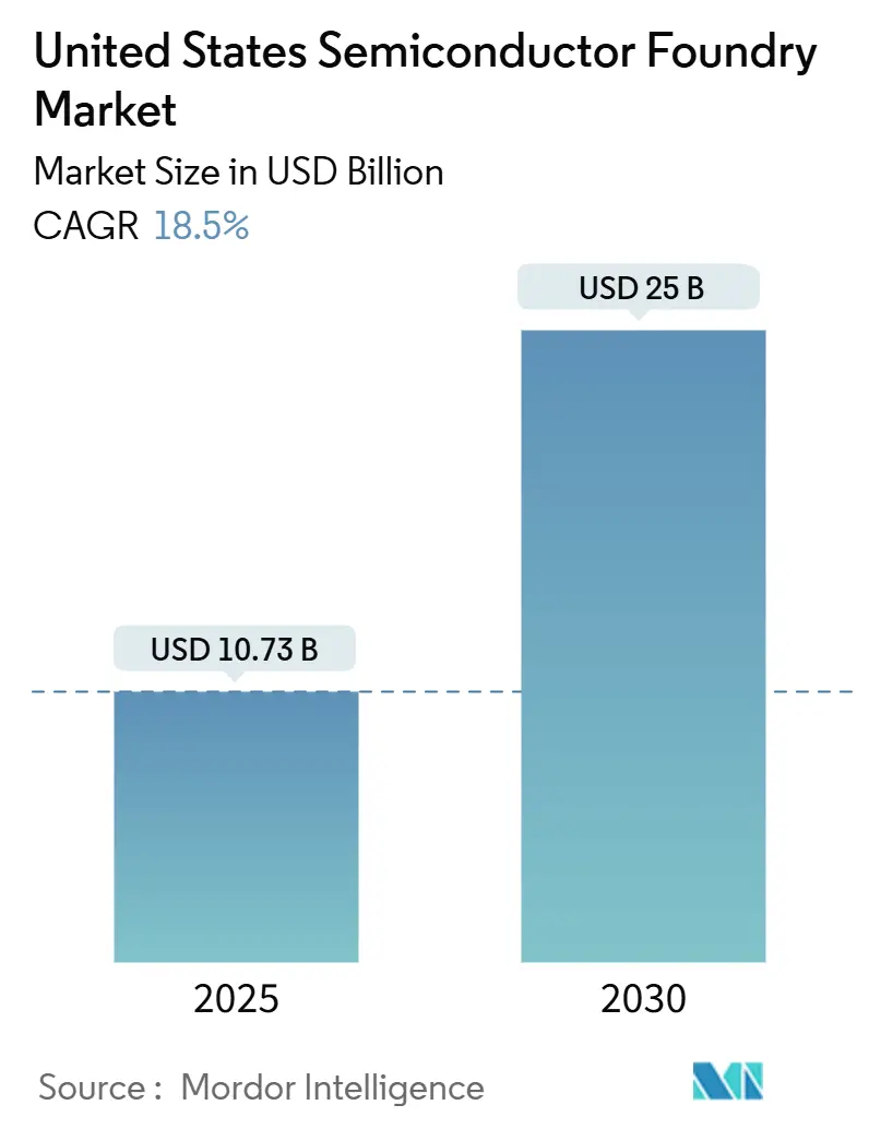
| Market Size (2025) | USD 10.73 Billion |
| Market Size (2030) | USD 25 Billion |
| Growth Rate (2025 - 2030) | 18.50% CAGR |
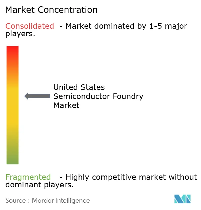
| Market Concentration | Medium |
Major Players
*Disclaimer: Major Players sorted in no particular order Image © Mordor Intelligence. Reuse requires attribution under CC BY 4.0. |
|
United States Semiconductor Foundry Market Analysis by Mordor Intelligence
The US semiconductor foundry market size is projected to grow from USD 10.73 billion in 2025 to USD 25 billion in 2030 at an 18.5% CAGR. Federal incentives under the CHIPS and Science Act, rising artificial-intelligence workloads that require sub-7 nm nodes, and persistent supply-chain rerouting have combined to accelerate domestic capacity additions. Strategic funding has lowered entry risks for new fabs, while the reshoring of advanced packaging services is tightening the link between design houses and local manufacturing. Automotive electrification is sustaining demand for mature 40-65 nm processes, and wide-bandgap power devices are opening incremental 200 mm opportunities. Competitive intensity is heightening as pure-play and IDM players court defense, automotive, and hyperscale customers with long-term volume contracts.
Key Report Takeaways
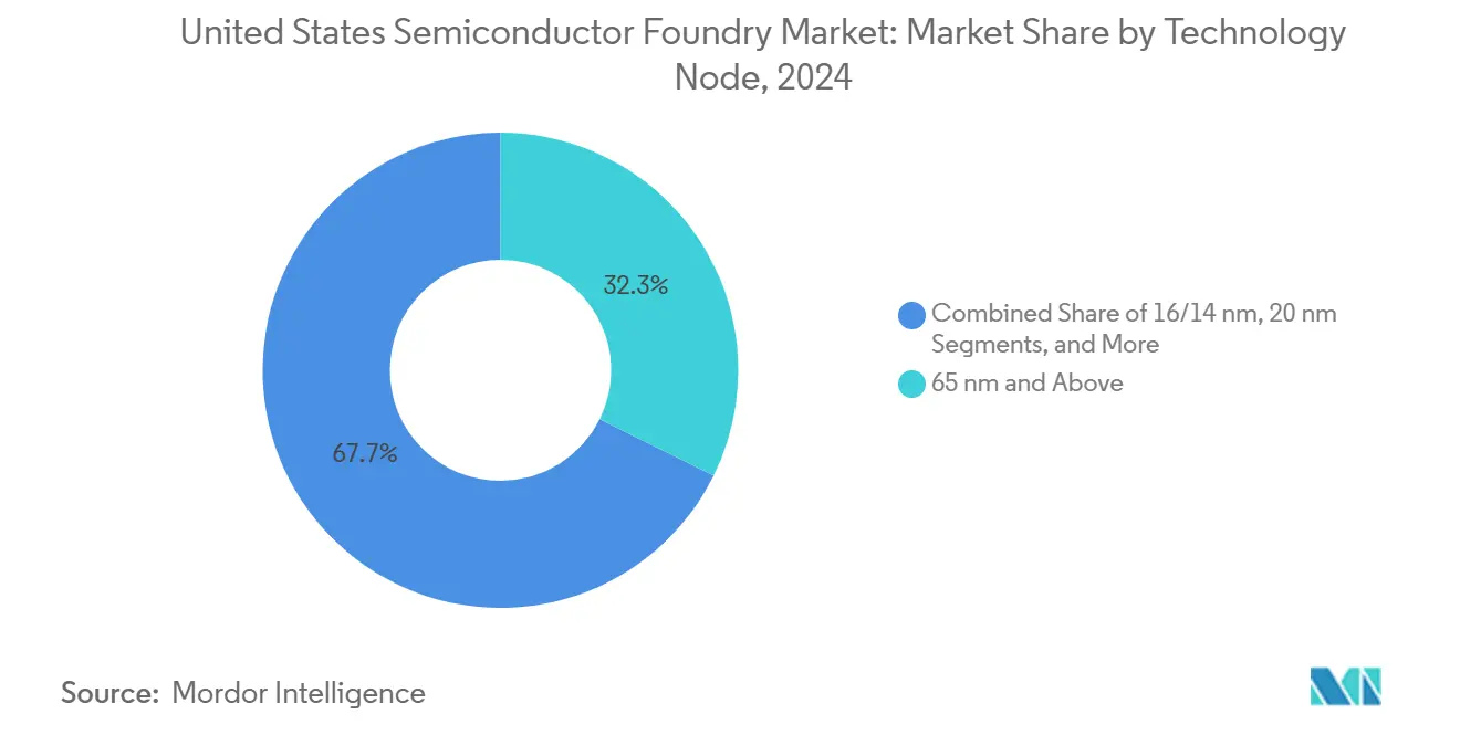
- By technology node, 65 nm and above processes led with 32.3% of the US semiconductor foundry market share in 2024, whereas the 10/7/5 nm-and-below tier is advancing at a 28.3% CAGR through 2030.
- By wafer size, 300 mm substrates accounted for a 68.6% share of the US semiconductor foundry market size in 2024, while 200 mm shipments are expanding at a 23.2% CAGR to 2030.
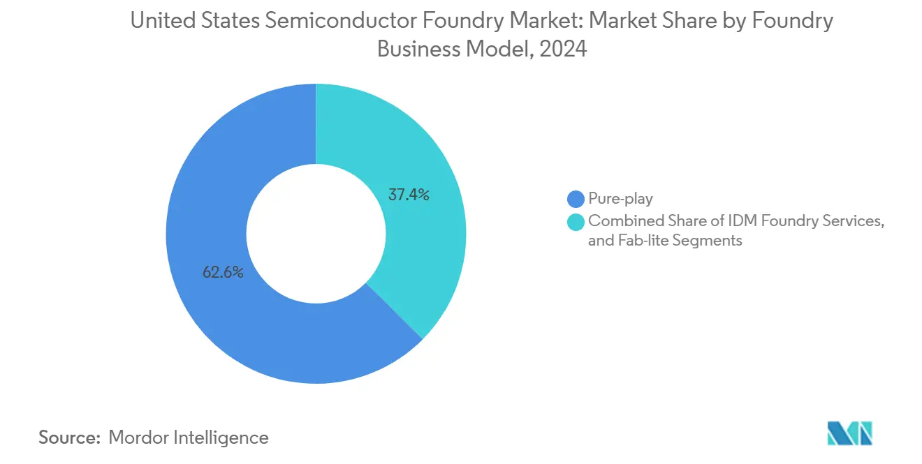
- By business model, pure-play operators held 62.6% of the US semiconductor foundry market share in 2024; IDM foundry services are registering the fastest 26.2% CAGR through 2030.
- By application, consumer electronics and communication captured 44.4% revenue in 2024, whereas high-performance computing is forecast to post a 29.1% CAGR to 2030.
United states operates as part of an interconnected international environment rather than as a self-contained country level unit. The semiconductor foundry market research by Mordor Intelligence places together all major developments across the globe within that wider frame.
United States Semiconductor Foundry Market Trends and Insights
Drivers Impact Analysis*
| Driver | (~) % Impact on CAGR Forecast | Geographic Relevance | Impact Timeline |
|---|---|---|---|
| CHIPS Act subsidies fueling domestic capacity expansion | +4.2% | National, concentrated in Arizona, Texas, New York, and Ohio | Medium term (2-4 years) |
| Accelerating AI/5G demand for advanced logic nodes | +5.8% | Global demand, US production focus on Arizona, Oregon | Short term (≤ 2 years) |
| Automotive shift to EV/ADAS requires reliable legacy nodes | +3.1% | National, with concentrations in Michigan, Texas, and California | Medium term (2-4 years) |
| Supply-chain resilience initiatives by U.S. OEMs | +2.7% | National, with emphasis on regional clusters | Long term (≥ 4 years) |
| DoD "trusted foundry" programs for secure IC sourcing | +1.9% | National, defense contractor regions | Long term (≥ 4 years) |
| GaN/SiC power devices opening niche 200 mm capacity | +1.8% | Regional, concentrated in specialized foundries | Medium term (2-4 years) |
| Source: Mordor Intelligence | |||
CHIPS Act Subsidies Fueling Domestic Capacity Expansion
Federal manufacturing incentives totaling USD 39 billion for new fabs and USD 11 billion for research have reset capital-allocation models across the domestic supply chain. TSMC’s USD 6.6 billion award for a third Phoenix fab anchors a USD 65 billion multistage investment that positions Arizona as the top advanced-node hub.[1]Taiwan Semiconductor Manufacturing Company, “TSMC Arizona and U.S. Department of Commerce Announce up to US$6.6 Billion in Proposed CHIPS Act Direct Funding,” pr.tsmc.com Intel’s parallel USD 20 billion Ohio project demonstrates how federal grants catalyze broader ecosystem build-out around tooling, chemicals, and workforce training. State incentives compound the effect; Arizona alone has attracted more than USD 102 billion in cumulative semiconductor commitments since 2020. Compliance clauses tied to workforce development and supply-chain transparency are reshaping fab operating models, encouraging closer collaboration between equipment vendors and universities.
Accelerating AI/5G Demand for Advanced Logic Nodes
Full utilization of overseas 3 nm capacity in 2024 confirmed the urgency of additional sub-7 nm lines, especially for AI accelerators and 5G processors. NVIDIA’s decision to assemble Blackwell GPUs in Phoenix through partnerships with TSMC and Foxconn reflects a pivot toward domestic advanced-node production for critical infrastructure. Advanced packaging requirements for chiplets and high-bandwidth memory are tightening the geographic link between wafer fabrication and backend integration. Localizing both front-end and advanced packaging minimizes logistics delays and satisfies emerging federal content rules for public-sector procurements.
Automotive Shift to EV/ADAS Requiring Reliable Legacy Nodes
Electric-vehicle semiconductor content has quadrupled since 2015, and AEC-Q100 reliability thresholds mandate stable, mature nodes. GlobalFoundries and NXP are co-developing 22FDX platforms optimized for automotive power efficiency and electromagnetic compatibility. The trend is spurring fresh 28/40/65 nm capacity investments inside the United States, where OEMs prefer geographically diversified supply after pandemic disruptions. Specialty foundries are also scaling 200 mm GaN and SiC lines suited to electric-drivetrain inverters, capitalizing on thermal performance advantages over silicon.
Supply-Chain Resilience Initiatives by US OEMs
The Department of Homeland Security has highlighted single-region dependencies for neon and hydrogen fluoride, prompting OEMs to adopt dual-sourcing mandates that include a domestic fab option. Defense primes are channeling trusted-foundry volumes through certified US sites, guaranteeing baseline demand even at premium pricing. Multiyear wafer-capacity agreements signed by consumer-electronics brands further derisk expansion projects and improve foundry revenue visibility.
Restraints Impact Analysis*
| Restraint | (~) % Impact on CAGR Forecast | Geographic Relevance | Impact Timeline |
|---|---|---|---|
| Multibillion-dollar capex barrier for leading-edge fabs | -2.8% | National, concentrated in high-cost regions | Long term (≥ 4 years) |
| Skilled workforce shortage in semiconductor manufacturing | -3.2% | National, acute in emerging clusters | Medium term (2-4 years) |
| Volatile critical-material supply (e.g., neon, HF) | -1.9% | Global supply, US production impact | Short term (≤ 2 years) |
| Environmental permitting delays and water-use constraints | -1.4% | Regional, concentrated in water-stressed areas | Medium term (2-4 years) |
| Source: Mordor Intelligence | |||
Multibillion-Dollar Capex Barrier for Leading-Edge Fabs
A single 5 nm fab demands USD 10-20 billion in equipment and construction, partly due to EUV systems that cost more than USD 200 million each.[2]ASML Holding N.V., “Annual Report 2024,” asml.com Even with a 25% federal grant, operators shoulder most costs, narrowing participation to capital-rich multinationals. Continuous two-year upgrade cycles compound the burden, locking smaller players out of cutting-edge nodes.
Skilled Workforce Shortage in Semiconductor Manufacturing
The industry faces a projected 67,000-worker shortfall by 2030, spanning process engineers, equipment technicians, and advanced-packaging specialists. Existing university output meets roughly one-third of annual demand, and visa limits restrict overseas hiring for defense-sensitive roles. State-led programs such as Arizona’s Future48 Workforce Accelerator are scaling but lag the pace of fab construction.
*Our forecasts treat driver/restraint impacts as directional, not additive. The impact forecasts reflect baseline growth, mix effects, and variable interactions.
Segment Analysis
By Technology Node: Revenue Anchored in Legacy, Growth in Sub-10 nm
Legacy processes secured 32.3% of the US semiconductor foundry market revenue in 2024, validating sustained demand for 65 nm and above nodes in power management, microcontrollers, and sensor hubs. Automotive and industrial clients value long qualification cycles and lower unit economics, keeping utilization high. A resilient tooling base and mature IP portfolios lower time-to-yield, which helps stabilize margins for pure-play operators.
The 10/7/5 nm-and-below tier is forecast to post a 28.3% CAGR, the fastest inside the US semiconductor foundry market. Growth stems from AI accelerators and flagship mobile processors that need maximum density and energy efficiency. Planned Arizona capacity will ship 2 nm wafers by 2028, positioning domestic fabs for a deeper share after the next node migration.


By Wafer Size: 300 mm Scale Meets 200 mm Specialty Demand
300 mm platforms commanded 68.6% of the US semiconductor foundry market size in 2024, driven by high-volume logic and memory production efficiencies. Advanced lithography tools, chemical-mechanical polishing, and metrology systems for sub-16 nm nodes are standardized around 300 mm substrates, reinforcing scale advantages.
Conversely, 200 mm lines are expanding at a 23.2% CAGR as power electronics, MEMS sensors, and RF switches migrate to wide-bandgap materials better suited to this diameter. Automotive OEMs lock in multi-year supply for SiC MOSFETs on 200 mm wafers, sustaining high mix-low volume demand profiles that larger 300 mm fabs cannot efficiently address.
By Foundry Business Model: Pure-Play Scale versus IDM Technology Depth
Pure-play operators held 62.6% of the US semiconductor foundry market share in 2024 thanks to a focus on manufacturing service excellence, quick cycle times, and neutrality toward customers. They thrive on differentiated offerings such as RF SOI or FDX nodes and advanced wafer-level packaging.
IDM foundry services, however, will grow fastest at a 26.2% CAGR. Giants like Intel monetize unused capacity and proprietary 18A technology while providing advanced packaging and test under one roof. Customers benefit from leading-edge process access combined with secure domestic supply, although concerns persist over IP firewalls during peak internal demand.
By Application: HPC Momentum Redefines Volume Mix
Consumer electronics and communication retained 44.4% revenue share in 2024 and continues to anchor baseline wafer starts for application processors, PMICs, and RF front-ends. Maturity of smartphone unit growth moderates its incremental contribution, yet refresh cycles for connectivity standards ensure steady tape-outs across node tiers.
High-performance computing will post the highest 29.1% CAGR as hyperscale and enterprise operators race to deploy AI clusters. Domestic capacity commitments by GPU vendors safeguard volume and align with federal guidelines for critical-infrastructure procurement, lifting the US semiconductor foundry market outlook for sub-5 nm nodes and advanced 2.5D packaging.
Geography Analysis
Arizona has consolidated the nation’s heaviest concentration of wafer fabrication commitments, surpassing USD 102 billion in cumulative project value since 2020. Three TSMC fabs, Intel’s Chandler expansions, and multiple supplier co-locations anchor an ecosystem supported by abundant solar power, streamlined permitting, and university talent pipelines.[3]Intel Corporation, “Intel Foundry Services,” intel.com The state’s semiconductor workforce surpassed 16,000 by mid-2025, and dedicated rail-served logistics hubs accelerate chemical supply deliveries.
Ohio emerged as a Midwest node following Intel’s USD 20 billion New Albany mega-site announcement. Access to Great Lakes water reserves, proximity to Detroit-area automotive OEMs, and bipartisan state incentives enhance competitiveness. Academic collaborations with Ohio State University underpin specialized curricula for lithography and equipment-maintenance roles, helping mitigate the national skill gap.
Texas maintains a legacy semiconductor presence in Austin and Dallas and is witnessing renewed momentum as Qorvo and other RF specialists relocate production. The state’s stable power grid and aerospace-defense customer base support growth in trusted foundry volumes and in specialty GaN RF devices. Further north, New York’s Malta facility forms the primary East Coast cluster, while Oregon’s mature yet aging fabs still provide trained labor pools and foundry diversification benefits.
Together, these regional clusters strengthen supply-chain resilience by distributing risk across climatic zones and critical-infrastructure footprints. Public-private workforce programs, water-recycling mandates, and renewable-energy purchase agreements are spreading as best practices that reduce operational friction for incoming investors.
The semiconductor foundry market is assessed by Mordor Intelligence through a multi-layered geographic lens, with detailed country-level analysis for Taiwan, Japan, Singapore, South Korea, Germany, China, Malaysia, and Israel.
Competitive Landscape
Domestic competition remains moderate with emerging consolidation pressures. GlobalFoundries leverages differentiated RF SOI and 22FDX automotive processes while expanding an Apple partnership that secures volume for power-efficient wireless chips.[4]GlobalFoundries, “GlobalFoundries Expands Partnership with Apple,” gf.com SkyWater Technology, certified under the DoD trusted-foundry framework, captures defense and aerospace demand for radiation-hardened designs. Intel Foundry Services positions advanced 18A gate-all-around technology and advanced packaging offerings as an integrated platform for cloud and automotive customers.
Strategic alliances have become central. TSMC collaborates with NVIDIA and Apple to co-locate advanced-node and CoWoS packaging lines in Arizona, ensuring tight design-to-fab feedback. Equipment suppliers such as ASML and Applied Materials are establishing local refurbishment centers to reduce downtime and align with domestic-content guidelines. Specialty players like X-FAB target SiC power devices and MEMS sensors, reinforcing niche leadership rather than pursuing leading-edge logic.
While the top five global foundries command over 80% of worldwide revenue, the US cohort is still ramping its share in advanced nodes. Sustained federal incentives, customer pre-payments, and supplier-financing mechanisms are expected to narrow the gap by the decade’s end.
United States Semiconductor Foundry Industry Leaders
-
GlobalFoundries Inc.
-
Intel Foundry Services
-
SkyWater Technology Inc.
-
X-FAB Texas Inc.
-
onsemi (Custom Foundry Services)
- *Disclaimer: Major Players sorted in no particular order

Recent Industry Developments
- August 2025: GlobalFoundries expanded its partnership with Apple to advance wireless connectivity and power-management technologies at the Malta, New York fab, reinforcing domestic chip leadership.
- August 2025: Qorvo confirmed the closure of its North Carolina factory, transitioning capacity to a new Texas site focused on defense and aerospace applications.
- August 2025: Infineon Technologies reported Q3 FY 2025 revenue of EUR 3.704 billion (USD 4.0 billion) and outlined priorities in software-defined vehicles and AI data centers.
- July 2025: NVIDIA began Blackwell AI chip production in Arizona through partnerships with TSMC, Foxconn, and Wistron, committing up to USD 500 billion for US manufacturing over four years.


United States Semiconductor Foundry Market Report Scope
| 10/7/5 nm and below |
| 16/14 nm |
| 20 nm |
| 28 nm |
| 45/40 nm |
| 65 nm and above |
| 300 mm |
| 200 mm |
| <150 mm |
| Pure-play |
| IDM Foundry Services |
| Fab-lite |
| Consumer Electronics and Communication |
| Automotive |
| Industrial and IoT |
| High-Performance Computing (HPC) |
| Other Applications |
| By Technology Node | 10/7/5 nm and below |
| 16/14 nm | |
| 20 nm | |
| 28 nm | |
| 45/40 nm | |
| 65 nm and above | |
| By Wafer Size | 300 mm |
| 200 mm | |
| <150 mm | |
| By Foundry Business Model | Pure-play |
| IDM Foundry Services | |
| Fab-lite | |
| By Application | Consumer Electronics and Communication |
| Automotive | |
| Industrial and IoT | |
| High-Performance Computing (HPC) | |
| Other Applications |


Key Questions Answered in the Report
How large is the US semiconductor foundry market in 2025?
The sector is valued at USD 10.73 billion and is forecast to reach USD 25 billion by 2030.
Which wafer size dominates US production capacity?
300 mm substrates hold 68.6% of shipments thanks to efficiency gains in advanced logic nodes.
What role does the CHIPS Act play in domestic capacity growth?
Federal incentives of USD 39 billion for fabs and USD 11 billion for R&D are accelerating new-fab construction and tooling upgrades.
Which application segment is growing fastest?
High-performance computing is projected to expand at a 29.1% CAGR, driven by AI accelerator demand.
Why are 200 mm fabs still relevant?
200 mm lines support GaN and SiC power devices and MEMS sensors that serve automotive and industrial markets.
What is the main talent challenge for US fabs?
A projected 67,000-worker shortage by 2030 threatens ramp schedules for new facilities and advanced packaging lines.
Page last updated on:


