Semiconductor Device Market Size and Share
Market Overview
| Study Period | 2019 - 2030 |
|---|---|
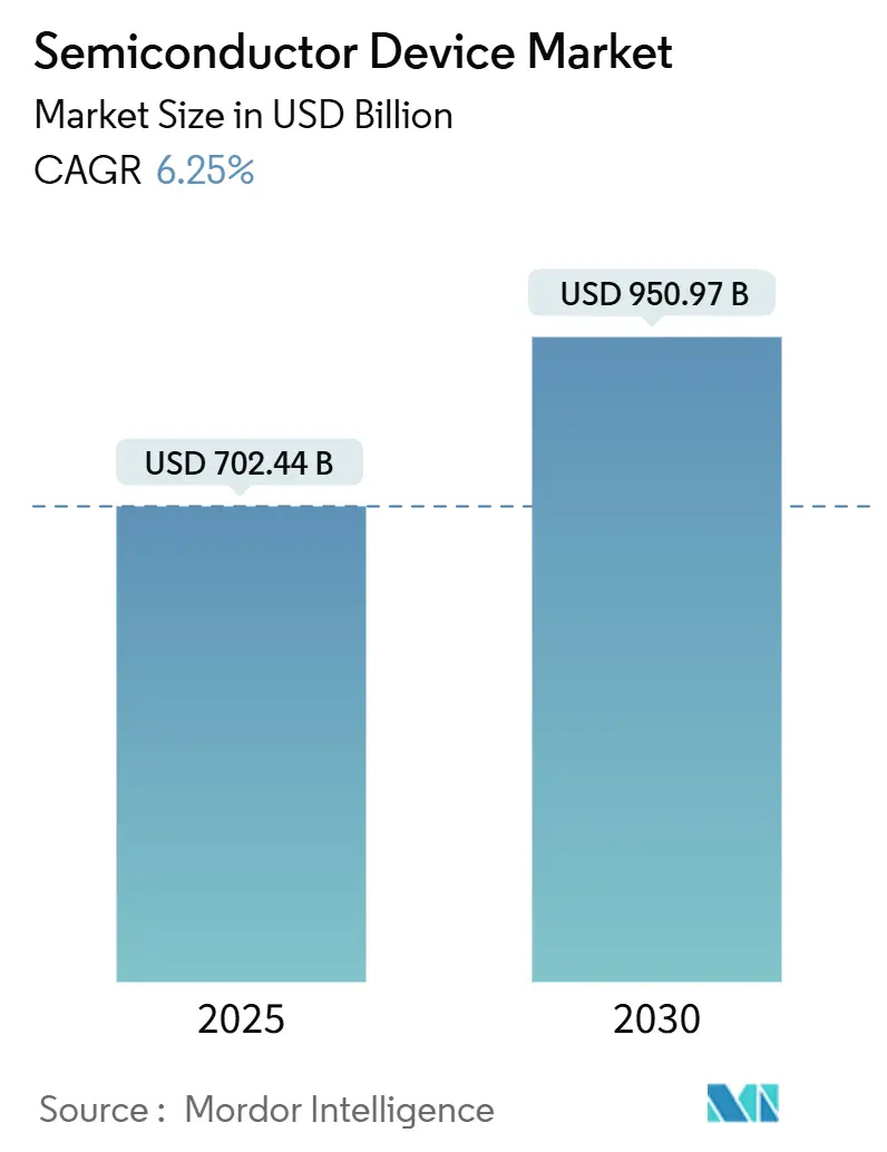
| Market Size (2025) | USD 702.44 Billion |
| Market Size (2030) | USD 950.97 Billion |
| Growth Rate (2025 - 2030) | 6.25% CAGR |
| Fastest Growing Market | Asia Pacific |
| Largest Market | Asia Pacific |
| Market Concentration | High |
Major Players*Disclaimer: Major Players sorted in no particular order Image © Mordor Intelligence. Reuse requires attribution under CC BY 4.0. | |
Semiconductor Device Market Analysis by Mordor Intelligence
The Semiconductor Device market size reached USD 702.44 billion in 2025 and is forecast to attain USD 950.97 billion by 2030, translating into a 6.25% CAGR over the period. Expanding demand for artificial-intelligence infrastructure, electric-vehicle powertrains, and industrial automation platforms keeps the semiconductor market on a multi-year growth trajectory. Hyperscale data-center owners are re-architecting server fleets around AI accelerators, while automakers raise silicon content per vehicle as they pivot to battery-electric drivetrains. Parallel government incentives in the United States, the European Union, and key Asian economies support new wafer-fab construction, yet lead-times for critical lithography tools remain a bottleneck. Geopolitical moves that reshape supply-chain footprints and regulatory compliance frameworks add complexity but also create strategic opportunities for firms that combine design leadership with resilient manufacturing partnerships.[1]TSMC Investor Relations, “TSMC Reports Fourth-Quarter 2024 Results,” tsmc.com
Key Report Takeaways
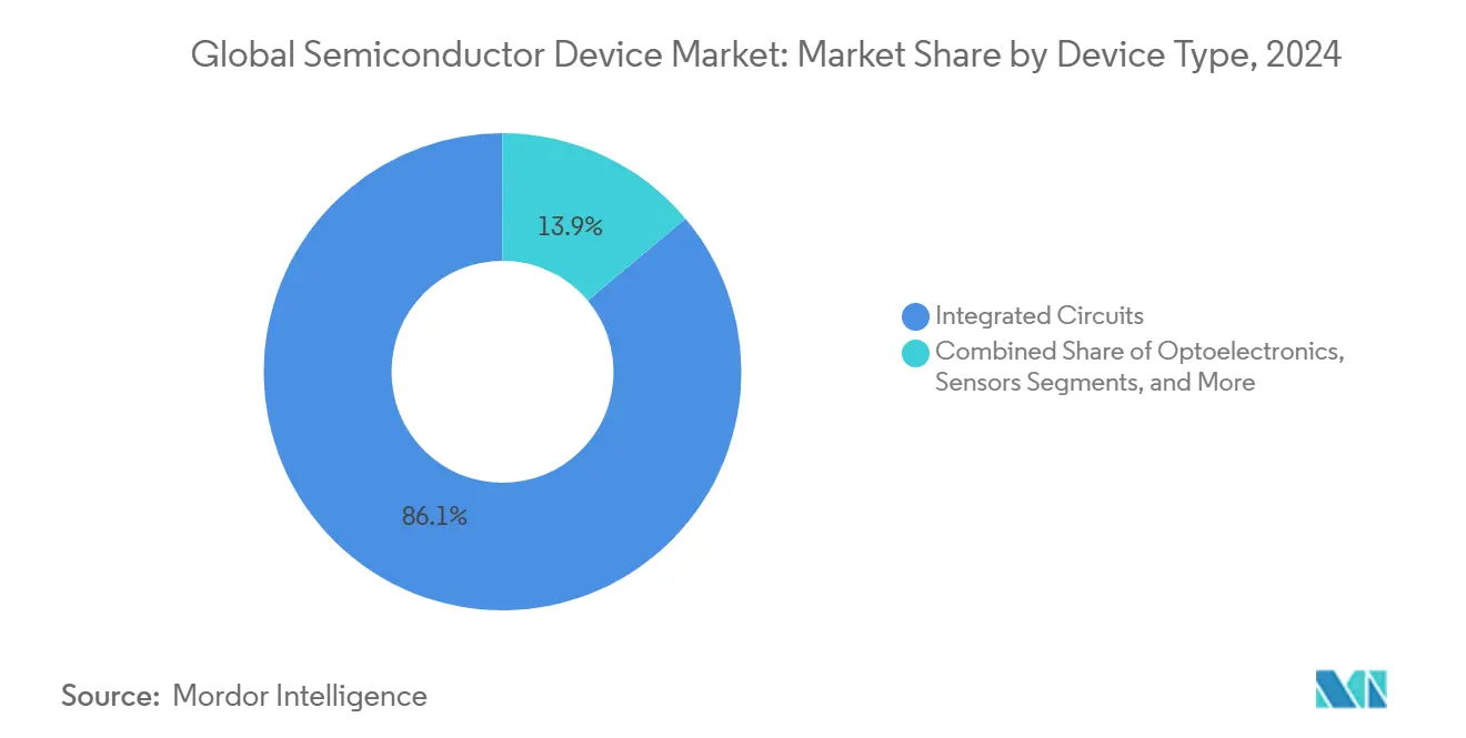
- By device type, integrated circuits accounted for 86.1% revenue share in 2024, and the category is poised for 7.9% CAGR through 2030, underscoring its dominance within the semiconductor market.
- By business model, design-centric and fabless vendors led with 66.5% of the semiconductor market share in 2024 and are projected to advance at an 8.3% CAGR over the forecast horizon.
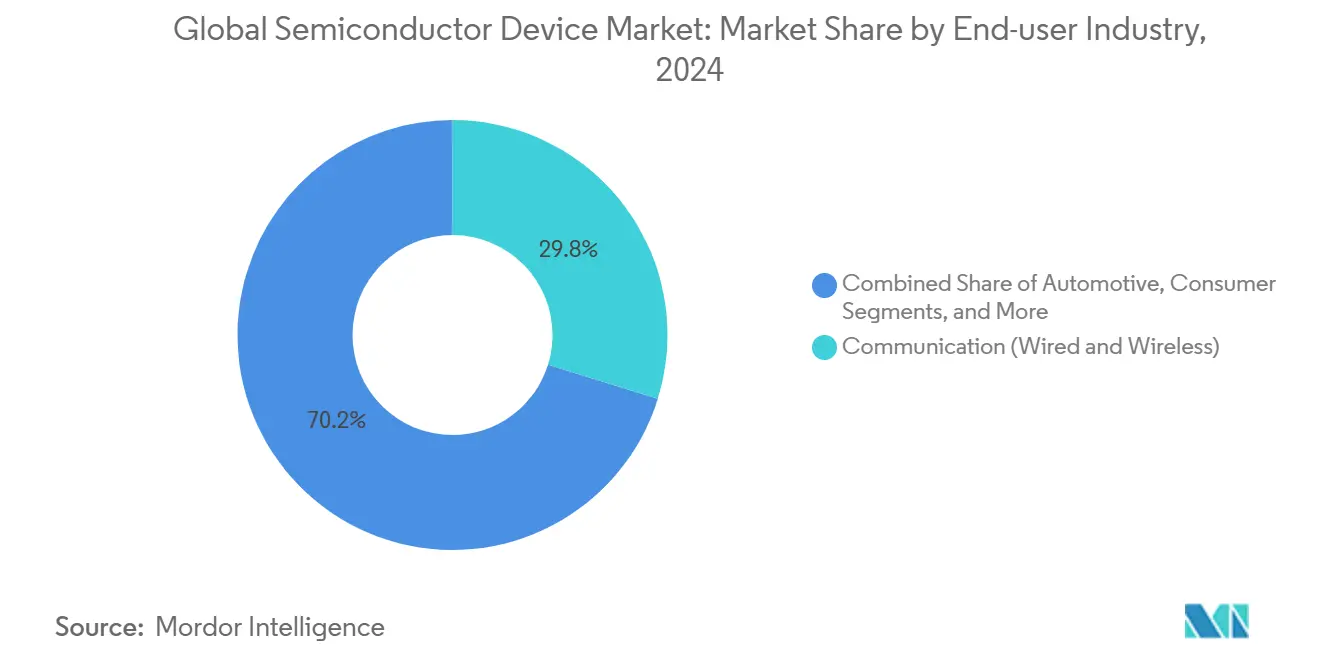
- By end-user industry, communication equipment held a 29.8% share in 2024, whereas AI-focused hardware is set to expand fastest at a 9.5% CAGR through 2030.
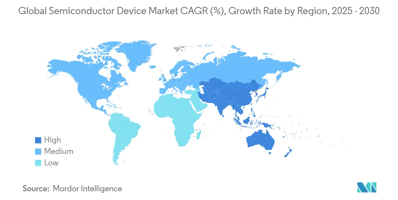
- By geography, Asia-Pacific captured 63.2% of the semiconductor market size in 2024 and is projected to grow at a 7.1% CAGR, maintaining its lead despite active diversification in North America and Europe.
Note: Market size and forecast figures in this report are generated using Mordor Intelligence’s proprietary estimation framework, updated with the latest available data and insights as of January 2026.
Global Semiconductor Device Market Trends and Insights
Drivers Impact Analysis*
| Driver | (~) % Impact on CAGR Forecast | Geographic Relevance | Impact Timeline |
|---|---|---|---|
| AI Accelerator Demand in Hyperscale Data Centers (US and China) | +1.8% | North America and China, spillover to Taiwan | Medium term (2-4 years) |
| EV Power-Electronics Content per Vehicle Surging | +1.2% | Global, with early gains in Europe, China, and North America | Long term (≥ 4 years) |
| ADAS Semiconductor Penetration in Next-Gen Vehicles | +0.9% | Global, led by Europe and North America, regulatory mandates | Medium term (2-4 years) |
| Industrial Edge-IoT Sensor Proliferation (Europe) | +0.7% | Europe core, spillover to North America and Asia-Pacific | Medium term (2-4 years) |
| 5G RF-Front-End Complexity (Korea and China) | +0.6% | Asia-Pacific core, particularly Korea and China | Short term (≤ 2 years) |
| US/EU CHIPS-Act Fab Incentives | +0.5% | North America and EU, indirect impact on Asia-Pacific | Long term (≥ 4 years) |
| Source: Mordor Intelligence | |||


AI accelerator demand in hyperscale data centers
Hyperscale operators in the United States and China are retrofitting server halls to support accelerator cards that draw over 1 kW each, prompting capital-expenditure plans topping USD 1 trillion by 2029. The shift requires custom silicon with high-bandwidth memory and advanced packaging, pushing foundry utilization above 90% at leading-edge nodes. The resulting backlog underlines why the semiconductor market continues to outpace earlier forecasts. Scarcity of advanced substrates and thermal-management materials further amplifies pricing power for suppliers.[2]Intel Newsroom, “Powering AI Everywhere: Intel Accelerated Roadmap Update,” intel.com
EV power-electronics content per vehicle surging.
Transition from internal-combustion to electric drivetrains lifts silicon content from roughly USD 600 to more than USD 2,000 per car. Silicon-carbide MOSFETs raise inverter efficiency by up to 3 percentage points, directly extending driving range. European automakers spearhead 800-V architectures, accelerating demand for wide-bandgap devices. The semiconductor market benefits from parallel growth in charging infrastructure that employs the same power modules.
ADAS semiconductor penetration in next-gen vehicles
Level 3+ autonomous features require real-time fusion of camera, radar, and lidar data, raising per-car semiconductor bill-of-materials above USD 1,500. Regulatory mandates in Europe and North America for advanced safety systems bolster adoption. Automotive-grade processors must meet stringent ISO 26262 requirements, creating high-margin niches for suppliers with functional-safety expertise. These dynamics reinforce the semiconductor market’s diversification beyond consumer electronics.[3]NXP Semiconductors, “Automotive Processing Solutions Portfolio,” nxp.com
Industrial edge-IoT sensor proliferation
European Industry 4.0 programs incentivize smart-factory rollouts that embed low-power sensors and microcontrollers on production lines. Demand centers on mixed-signal chips that pair analog front ends with MCU cores and wireless connectivity, enabling local analytics and reducing cloud latency. Suppliers that integrate sensor fusion and security IP blocks capture design-win momentum. Resultant volume supports capacity utilization at mature nodes, balancing the semiconductor market across process generations.
Restraints Impact Analysis*
| Restraint | (~) % Impact on CAGR Forecast | Geographic Relevance | Impact Timeline |
|---|---|---|---|
| Lithography Tool Lead-Times >18 Months | -1.1% | Global, particularly affecting advanced node capacity | Medium term (2-4 years) |
| Export-Control Curbs on Advanced Nodes (China) | -0.8% | China's core indirect impact on global supply chains | Short term (≤ 2 years) |
| High Fab Capex and Energy Intensity | -0.6% | Global, concentrated in advanced manufacturing regions | Long term (≥ 4 years) |
| Engineering-Talent Shortage | -0.4% | Global, acute in North America, Europe, and the Asia-Pacific | Long term (≥ 4 years) |
| Source: Mordor Intelligence | |||
Lithography tool lead times> 18 months
High-NA extreme-ultraviolet steppers priced near USD 380 million each face production bottlenecks, with deliveries stretching beyond 18 months. Limited tool availability caps capacity additions even as demand for 3 nm-and-below processes climbs. Early tool recipients obtain temporary pricing leverage, while laggards risk design wins migrating to competitors. Prolonged supply gaps temper the semiconductor market’s otherwise strong growth outlook.
Export-control curbs on advanced nodes
Expanded U.S. controls restrict the sale and support of machinery capable of sub-16 nm production to Chinese fabs. Domestic firms in China pivot to mature-node output, crowding older process lines and raising global legacy-chip pricing. Non-Chinese customers fear interruptions and diversify sourcing, influencing capital-allocation decisions across the semiconductor market. Retaliatory measures on gallium and germanium exports inject additional volatility.[4]U.S. Department of Commerce, “Export Administration Regulations – October 2024 Update,” commerce.gov
*Our forecasts treat driver/restraint impacts as directional, not additive. The impact forecasts reflect baseline growth, mix effects, and variable interactions.
Segment Analysis
By Device Type: Integrated Circuits Sustain Leadership
Integrated circuits captured 86.1% of the semiconductor market in 2024 and are projected to advance at a 7.9% CAGR through 2030. Logic and analog sub-segments gain from AI inference engines, vehicle-electrification control, and industrial automation rollouts. High-bandwidth memory and 3-D NAND remain cornerstones of AI accelerator performance, reinforcing premium pricing. Discrete power devices, optoelectronics, and sensors, though smaller in dollar terms, enable system-level functionality vital for EV inverters and optical-communication modules. Silicon-carbide MOSFETs and gallium-nitride HEMTs post double-digit volume gains, reflecting drivetrain voltage escalation trends. MEMS inertial and environmental sensors proliferate in Industry 4.0 projects, ensuring balanced growth across device classes. These trends collectively position integrated circuits at the forefront of the semiconductor market size expansion while permitting specialized components to capture emerging niches.


By Business Model: Fabless Specialization Accelerates Innovation
Design-centric and fabless entities controlled 66.5% of revenue in 2024 and are on track for an 8.3% CAGR through 2030, the fastest among business models. Separation of design and manufacturing lets fabless firms iterate architectures swiftly, a critical factor in AI accelerator races where performance leaps materialize annually. Access to multiproject wafer programs lowers tape-out barriers for start-ups, fueling ecosystem vitality. Integrated-device manufacturers retain advantages in analog and power portfolios where process know-how is tightly linked to materials science, yet face capex pressures surpassing USD 20 billion per node. Emergent foundry–fabless collaboration on advanced packaging redefines value capture, as system-in-package solutions compress board-level designs. This structural evolution reinforces the semiconductor market’s inclination toward innovation-driven differentiation rather than pure capacity scale.
By End-user Industry: AI Outpaces Communication in Growth
Communication infrastructure remained the largest contributor with a 29.8% share in 2024, sustained by 5 G base-station rollouts and fiber backbone upgrades. Conversely, AI compute nodes spanning data centers to edge appliances exhibit the highest growth at 9.5% CAGR, commanding premium average-selling-price chips that significantly enlarge the semiconductor market size for accelerator-class silicon. Automotive demand intensifies as battery-electric and ADAS content rise, while industrial automation integrates machine-vision processors and real-time MCUs. Consumer electronics moderate after pandemic-era peaks, but premium smartphones incorporating AI co-processors prevent unit declines. Government and aerospace orders prioritize radiation-hardened devices, creating small yet high-margin pockets. Diversified application spread shields the semiconductor market from single-segment downturns, albeit heightening design-win complexity for suppliers.
Geography Analysis
Asia-Pacific commanded 63.2% of global revenue in 2024 and is forecast to grow at a 7.1% CAGR to 2030, anchored by Taiwan’s advanced-node leadership and South Korea’s USD 471 billion megacluster build-out. Mainland China, while constrained at leading nodes, invests heavily in mature-process parks and domestic equipment suppliers, aiming to lift local content ratios. Japan channels ¥3.9 trillion (USD 26.1 billion) into joint ventures that couple domestic materials prowess with external foundry expertise, while India accelerates assembly-test and design-services growth.
North America ranks second by value, catalyzed by USD 52 billion CHIPS Act incentives that underwrite new fabs in Arizona, Ohio, and Texas. Intel secured USD 7.865 billion, TSMC USD 6.6 billion, and Samsung USD 4.745 billion for U.S. expansions. The region houses a dense cluster of fabless AI and networking chip designers, translating into sustained demand for advanced wafers. Automotive electrification programs in Michigan and California further diversify revenue streams, ensuring the semiconductor market remains robust even amid cyclical consumer-electronics swings. Section 5949 of the 2023 NDAA will phase in procurement restrictions in 2027, nudging supply chains toward domestic nodes for defense-linked workloads.
Europe, holding under 10% share, nonetheless influences technology direction through stringent automotive and environmental regulations that shape chip specifications worldwide. The EU Chips Act targets a 20% production share by 2030 via incentive pools for Dresden and Eindhoven projects focusing on power electronics and specialty analog. Germany anchors premium vehicle semiconductor demand, while Nordic grids adopt wide-bandgap devices for renewables. Collaborative R&D alliances leverage university-industry ties, positioning the continent as a competence center for reliability and safety certification—attributes prized across the semiconductor market.
Mordor Intelligence provides coverage of the semiconductor device market across other key regional markets, including Asia and Europe, each with their regulatory frameworks and demand patterns. Detailed country-level analysis extends to South Korea, China, and Japan incorporating local coverage and market participation, as required.

Competitive Landscape
Foundry capacity remains highly concentrated; the top 10 players controlled the majority of output in 2024. TSMC led the market, leveraging high-volume 3 nm ramps and superior packaging services. Samsung held a significant revenue share but struggles with advanced-node yields, recently courting automotive customers to diversify its mix. GlobalFoundries and UMC are exploring a merger that would create a multiregional player with combined revenue topping USD 15 billion, raising competitive stakes in specialty and mature nodes.
Strategic pivots emphasize vertical collaboration: Intel and TSMC formed an advanced-packaging joint venture, combining substrate integration expertise with leading-edge wafer output. Synopsys-Ansys’s USD 35 billion union consolidates simulation and EDA tool chains, shortening chip-validation cycles. Suppliers of specialty materials, such as 3M, join U.S. consortia to localize substrate and thermal interface production, addressing geopolitical supply-risk concerns.
The talent gap looms large; forecasts show 58% of incremental engineering roles could remain unfilled by 2030, compelling firms to establish apprenticeship pipelines and AI-assisted design flows. Export-control regimes intensify compliance overheads but simultaneously shelter incumbents with transparent value chains. Overall, competitive advantage accrues to companies blending design agility, manufacturing access, and regulatory fluency, reinforcing the semiconductor market’s oligopolistic profile.
Semiconductor Device Industry Leaders
Intel Corporation
Nvidia Corporation
Kyocera Corporation
Qualcomm Incorporated
STMicroelectronics NV
- *Disclaimer: Major Players sorted in no particular order

Recent Industry Developments
- August 2025: Tesla and Samsung Electronics finalized a USD 16.5 billion alliance for autonomous-driving AI chips, with Samsung providing high-bandwidth memory and advanced packaging.
- July 2025: GlobalFoundries announced a USD 16 billion U.S. capacity expansion to boost mature-node output 40% by 2028, inclusive of automotive-qualified lines.
- June 2025: TSMC commenced commercial 2 nm production in Taiwan, securing initial orders from Apple and Nvidia.
- April 2025: Intel and TSMC launched a joint venture on next-generation packaging, sharing IP and process-development roadmaps.


Global Semiconductor Device Market Report Scope
Semiconductor devices are electronic components made from semiconductor materials that exhibit unique electrical properties. Semiconductor materials, such as silicon and germanium, have the unique characteristic of conducting electricity under certain conditions. Unlike conductors (like metals) that easily allow the flow of electrons and insulators (like rubber) that resist the flow of electrons, semiconductors have conductivity that can be controlled.
The market is defined by the revenue generated from sales of semiconductor devices like discrete semiconductors, optoelectronics, sensors, and integrated circuits comprising analog, logic, memory, and micro-integrated circuits employed in various end-user verticals like automotive, communication (wired, wireless), consumer, industrial, computing/data storage, government (aerospace & defense), etc., across various countries like United States, Europe, Japan, China, Korea, Taiwan, and Rest of the World.
The semiconductor device market is segmented by device type (discrete semiconductors, optoelectronics, sensors, integrated circuits (analog, logic, memory, micro [microprocessors (MPU), microcontrollers (MCU), digital signal processors]), by end-user application (automotive, communication (wired and wireless), consumer, industrial, computing/data storage, government (aerospace and defense)), and geography (United States, Europe, Japan, China, Korea, Taiwan, Rest of the World). The report offers market forecasts and size in volume (units) and value (USD) for all the above segments.
| Discrete Semiconductors | Diodes | ||
| Transistors | |||
| Power Transistors | |||
| Rectifier and Thyristor | |||
| Other Discrete Devices | |||
| Optoelectronics | Light-Emitting Diodes (LEDs) | ||
| Laser Diodes | |||
| Image Sensors | |||
| Optocouplers | |||
| Other Device Types | |||
| Sensors and MEMS | Pressure | ||
| Magnetic Field | |||
| Actuators | |||
| Acceleration and Yaw Rate | |||
| Temperature and Others | |||
| Integrated Circuits | By Integrated Circuit Type | Analog | |
| Micro | Microprocessors (MPU) | ||
| Microcontrollers (MCU) | |||
| Digital Signal Processors | |||
| Logic | |||
| Memory | |||
| By Technology Node (Shipment Volume Not Applicable) | < 3nm | ||
| 3nm | |||
| 5nm | |||
| 7nm | |||
| 16nm | |||
| 28nm | |||
| > 28nm | |||
| IDM |
| Design/ Fabless Vendor |
| Automotive |
| Communication (Wired and Wireless) |
| Consumer |
| Industrial |
| Computing/Data Storage |
| Data Center |
| AI |
| Government (Aerospace and Defense) |
| North America | United States | |
| Canada | ||
| Mexico | ||
| South America | Brazil | |
| Mexico | ||
| Argentina | ||
| Rest of South America | ||
| Europe | Germany | |
| France | ||
| United Kingdom | ||
| Nordics | ||
| Rest of Europe | ||
| Asia-Pacific | China | |
| Taiwan | ||
| South Korea | ||
| Japan | ||
| India | ||
| Rest of Asia-Pacific | ||
| Middle East and Africa | Middle East | Saudi Arabia |
| United Arab Emirates | ||
| Turkey | ||
| Rest of Middle East | ||
| Africa | South Africa | |
| Rest of Africa | ||
| By Device Type (Shipment Volume for Device Type is Complementary) | Discrete Semiconductors | Diodes | ||
| Transistors | ||||
| Power Transistors | ||||
| Rectifier and Thyristor | ||||
| Other Discrete Devices | ||||
| Optoelectronics | Light-Emitting Diodes (LEDs) | |||
| Laser Diodes | ||||
| Image Sensors | ||||
| Optocouplers | ||||
| Other Device Types | ||||
| Sensors and MEMS | Pressure | |||
| Magnetic Field | ||||
| Actuators | ||||
| Acceleration and Yaw Rate | ||||
| Temperature and Others | ||||
| Integrated Circuits | By Integrated Circuit Type | Analog | ||
| Micro | Microprocessors (MPU) | |||
| Microcontrollers (MCU) | ||||
| Digital Signal Processors | ||||
| Logic | ||||
| Memory | ||||
| By Technology Node (Shipment Volume Not Applicable) | < 3nm | |||
| 3nm | ||||
| 5nm | ||||
| 7nm | ||||
| 16nm | ||||
| 28nm | ||||
| > 28nm | ||||
| By Business Model | IDM | |||
| Design/ Fabless Vendor | ||||
| By End-user Industry | Automotive | |||
| Communication (Wired and Wireless) | ||||
| Consumer | ||||
| Industrial | ||||
| Computing/Data Storage | ||||
| Data Center | ||||
| AI | ||||
| Government (Aerospace and Defense) | ||||
| By Geography | North America | United States | ||
| Canada | ||||
| Mexico | ||||
| South America | Brazil | |||
| Mexico | ||||
| Argentina | ||||
| Rest of South America | ||||
| Europe | Germany | |||
| France | ||||
| United Kingdom | ||||
| Nordics | ||||
| Rest of Europe | ||||
| Asia-Pacific | China | |||
| Taiwan | ||||
| South Korea | ||||
| Japan | ||||
| India | ||||
| Rest of Asia-Pacific | ||||
| Middle East and Africa | Middle East | Saudi Arabia | ||
| United Arab Emirates | ||||
| Turkey | ||||
| Rest of Middle East | ||||
| Africa | South Africa | |||
| Rest of Africa | ||||


Key Questions Answered in the Report
What is the projected value of the semiconductor device market by 2030?
The global sector is forecast to reach USD 950.97 billion by 2030.
How fast will AI hardware grow compared with traditional communication chips?
AI-focused semiconductor sales are projected to rise at a 9.5% CAGR, outpacing the communication segment’s steady expansion.
Why are integrated circuits central to future revenue?
Integrated circuits hold 86.1% share and are advancing at 7.9% CAGR due to their role in AI, automotive, and industrial platforms.
Which region will expand semiconductor device output the most?
Asia-Pacific retains a 63.2% share and leads growth at a 7.1% CAGR, driven by Taiwan, South Korea, and China investments.
How do government incentives affect chip-supply resilience?
U.S. and EU CHIPS Acts channel billions into local fabs, diversifying supply and easing regulatory barriers for domestic procurement.
Page last updated on:


