GPU And HPC Silicon Interposer Market Size and Share
Market Overview
| Study Period | 2020 - 2031 |
|---|---|
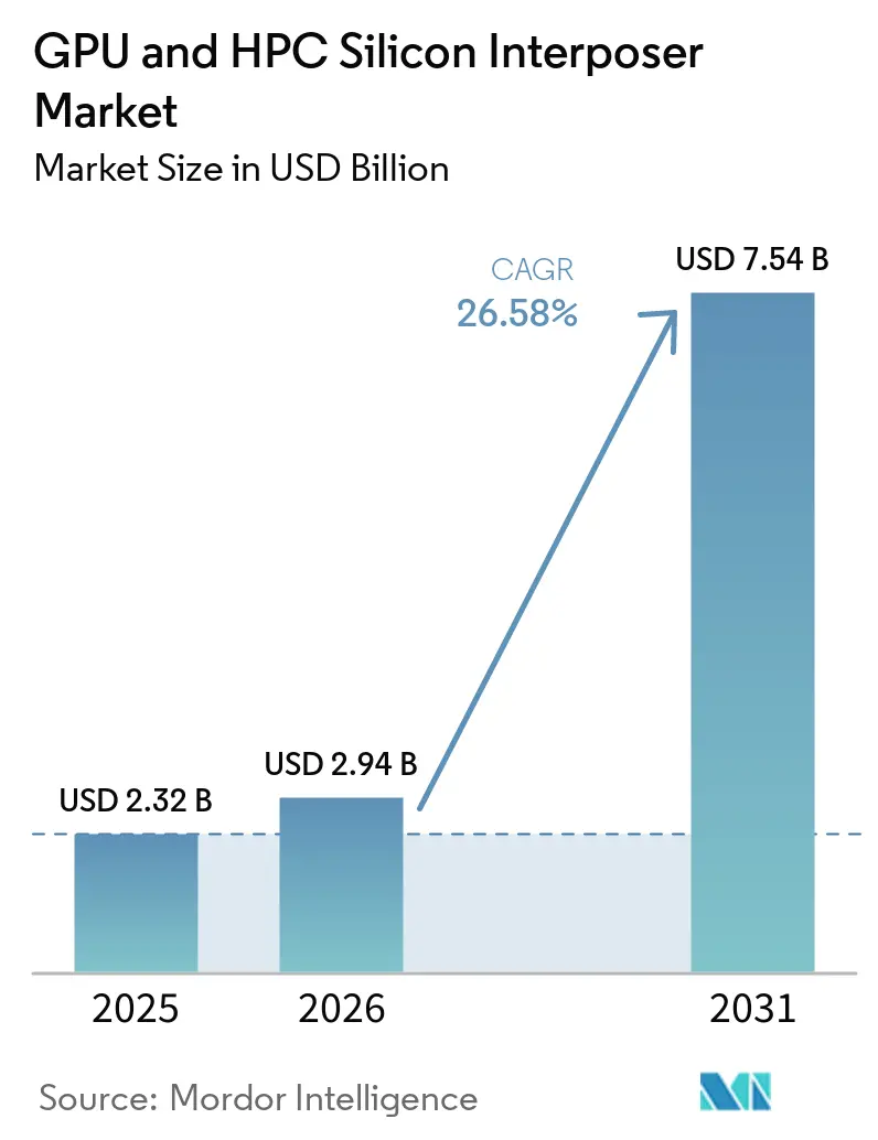
| Market Size (2026) | USD 2.94 Billion |
| Market Size (2031) | USD 7.54 Billion |
| Growth Rate (2026 - 2031) | 26.58% CAGR |
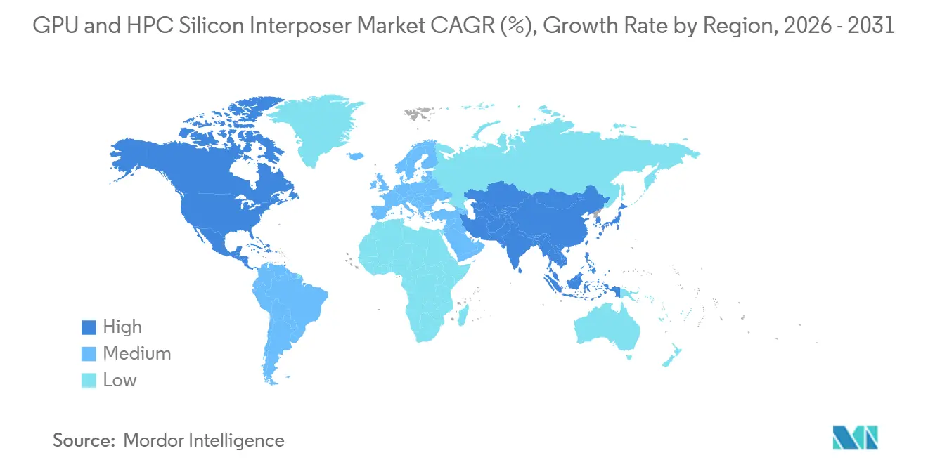
| Fastest Growing Market | Asia-Pacific |
| Largest Market | North America |
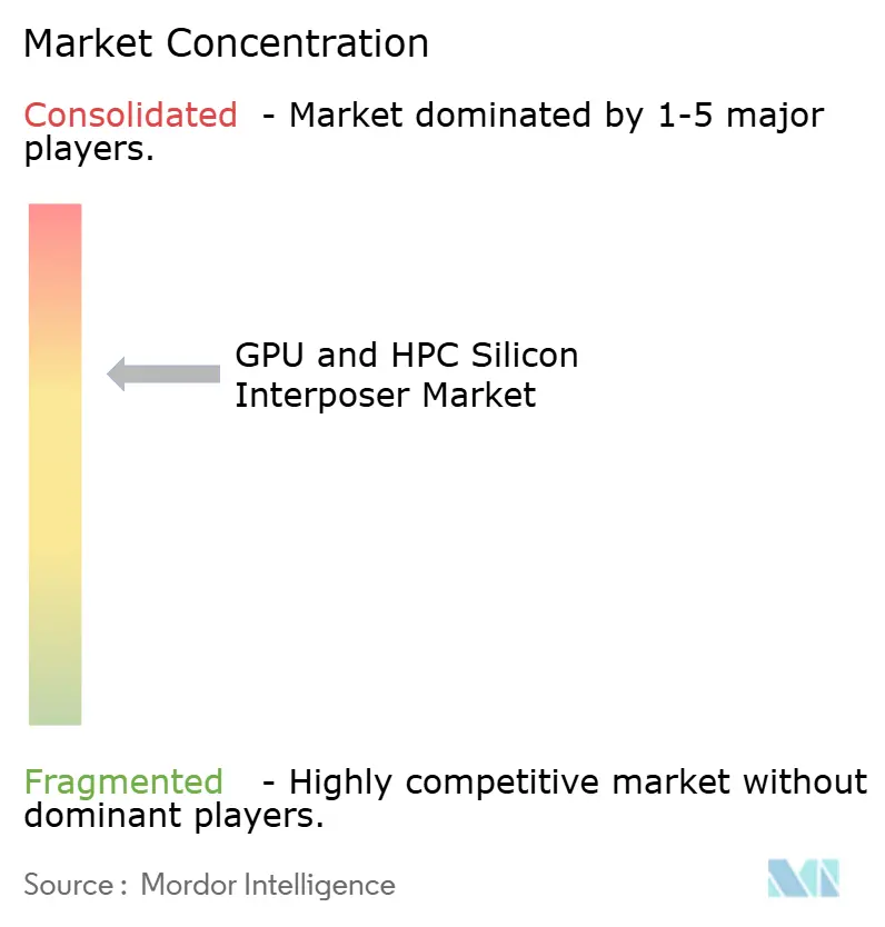
| Market Concentration | Medium |
Major Players *Disclaimer: Major Players sorted in no particular order Image © Mordor Intelligence. Reuse requires attribution under CC BY 4.0. | |
GPU And HPC Silicon Interposer Market Analysis by Mordor Intelligence
The GPU and HPC silicon interposer market size is expected to increase from USD 2.32 billion in 2025 to USD 2.94 billion in 2026 and reach USD 7.54 billion by 2031, growing at a CAGR of 26.58% over 2026-2031. Unprecedented demand for generative-AI compute, escalating HBM stack counts, and the move toward chiplet-based architectures are pushing organic substrates beyond their physical limits, making large-area silicon interposers the default bridge between logic and memory. TSMC’s Chip-on-Wafer-on-Substrate (CoWoS) capacity remains fully booked, while Samsung, ASE Technology, and Amkor Technology are accelerating multibillion-dollar expansion programs to close the supply gap. Simultaneously, hyperscalers are locking in long-term contracts to de-risk their AI roadmaps, and equipment lead times for through-silicon-via (TSV) tooling have stretched to more than 18 months. Packaging roles are also shifting, as power-delivery networks, retimers, and voltage regulators migrate onto the interposer plane, reshaping bill-of-materials economics for USD 30,000-plus accelerators.
Key Report Takeaways
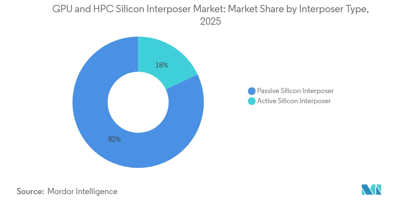
- By interposer type, passive silicon variants commanded 82% of the GPU and HPC silicon interposer market share in 2025, while active designs is expected to advance at a 26.98% CAGR through 2031.
- By application, AI and machine-learning accelerators led with 48% revenue share in 2025 and is expected to expand at a 27.38% CAGR through 2031.
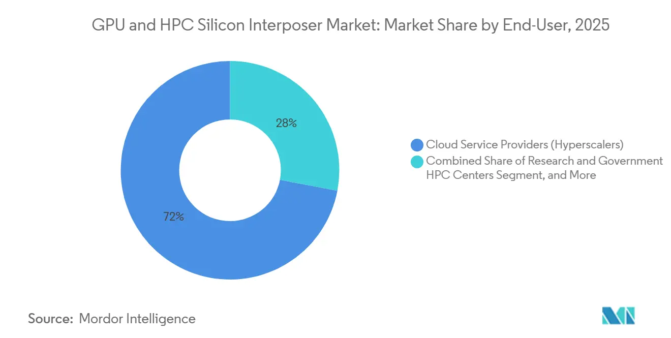
- By end-user, cloud service providers accounted for 72% of demand in 2025, whereas enterprise data centers are set to grow at a 27.43% CAGR through 2031.
- By geography, Asia-Pacific captured a 65% share in 2025, but North America is forecast to register the fastest CAGR of 27.58% through 2031.
Note: Market size and forecast figures in this report are generated using Mordor Intelligence’s proprietary estimation framework, updated with the latest available data and insights as of January 2026.
Global GPU And HPC Silicon Interposer Market Trends and Insights
Drivers Impact Analysis*
| Driver | (~) % Impact on CAGR Forecast | Geographic Relevance | Impact Timeline |
|---|---|---|---|
| Rapid Proliferation of Generative AI Workloads | +8.5% | Global, concentrated in North America and Asia-Pacific | Short term (≤ 2 years) |
| Escalating HBM Stack Counts Per GPU Package | +7.2% | Taiwan and South Korea production hubs | Medium term (2-4 years) |
| Transition Toward Chiplet-Based GPU Architectures | +5.8% | North America and Europe design, Asia-Pacific manufacturing | Medium term (2-4 years) |
| Mainstream Adoption of 2.5D Packages in Networking ASICs | +3.1% | Global early adoption in hyperscale data centers | Medium term (2-4 years) |
| Wafer-Scale Fabrication Yield Improvements | +1.4% | Asia-Pacific foundry operations | Long term (≥ 4 years) |
| Growing Use of Lateral Power-Delivery Networks | +0.8% | North America and Asia-Pacific advanced packaging lines | Long term (≥ 4 years) |
| Source: Mordor Intelligence | |||
Rapid Proliferation Of Generative AI Workloads
Frontier models now exceed one trillion parameters and demand memory bandwidth above 20 TB/s, a threshold only attainable with large-area silicon interposers. NVIDIA’s Blackwell architecture ships in volume during 2026 with eight HBM3E stacks delivering 18 TB/s, forcing package footprints beyond 3,500 mm². The pivot from training-centric to inference-dominant deployments prioritizes memory capacity and latency over sheer compute density, as illustrated by Microsoft’s Maia 100 and Google’s TPU v5p, both launched in 2025. Hyperscalers’ custom silicon is fragmenting the GPU and HPC silicon interposer market, because every proprietary accelerator requires its own CoWoS allocation, keeping demand high even if GPU unit growth moderates. Consequently, interposer suppliers enjoy multi-year visibility but must juggle small-lot custom designs, which complicate line utilization.[1]NVIDIA Corp., “NVIDIA Blackwell Platform Arrives to Power a New Era of Computing,” NVIDIA Newsroom, nvidianews.nvidia.com
Escalating HBM Stack Counts Per GPU Package
HBM integration has doubled from four stacks in 2022 to eight in 2025, with 12-stack roadmaps on track for 2028. Each additional stack multiplies TSV density and amplifies thermal gradients across die sizes, surpassing 2,000 mm². TSMC’s CoWoS-L, introduced in 2024, partitions logic and memory zones to enable 12-stack layouts without breaching 400-W thermal envelopes, while SK Hynix began volume shipments of 12-high HBM3E in 2025. Memory-side bottlenecks remain acute, as three vendors still command 95% of HBM capacity, creating ripple effects that propagate into interposer wafer planning.
Transition Toward Chiplet-Based GPU Architectures
Disaggregating monolithic dies cuts cost and boosts yield, a strategy pioneered by AMD’s MI300 in 2024, which mixed 5-nm compute chiplets with 6-nm I/O dies on a shared interposer and trimmed manufacturing bills by up to 40%. Intel’s 47-tile Ponte Vecchio showed the approach scales, yet Intel’s decision to postpone Falcon Shores in favor of rack-scale Jaguar Shores underlines practical package limits. Chiplet schemes require interposers that support multiterabit die-to-die links with sub-nanosecond latency, accelerating the adoption of open standards such as UCIe 2.0. The flexibility comes at a planning cost, foundries must reserve multiple die sizes, straining photomask capacity and slowing ramp economics.
Mainstream Adoption Of 2.5D Packages In Networking ASICs
The migration to 800-G and 1.6-T Ethernet has spawned networking ASICs that embed a dozen HBM stacks next to switching logic. Broadcom’s Tomahawk 6, shipping in 2026, consolidates 102.4 Tb/s of switching on an interposer over 6,000 mm², slashing power per bit by an order of magnitude compared with organic substrates. Marvell’s Teralynx 11 employs 2-nm process nodes and 3-D bidirectional I/O at 6.4 Gb/s, targeting non-blocking fabrics for GPU mega-clusters. Because network refresh cycles run on three-to-five-year cadences regardless of AI booms, interposer demand in this segment brings welcome stability to outsourced semiconductor assembly and test (OSAT) houses.
Restraints Impact Analysis*
| Restraint | (~) % Impact on CAGR Forecast | Geographic Relevance | Impact Timeline |
|---|---|---|---|
| Limited Foundry Capacity For ≥65 K mm² Interposers | -3.8% | Taiwan and South Korea | Short term (≤ 2 years) |
| High Build-Up Substrate Costs Offsetting Savings | -2.2% | Asia-Pacific supply chains | Medium term (2-4 years) |
| Reliability Concerns In Large-Area Passive Silicon | -1.1% | Global HPC and automotive fields | Medium term (2-4 years) |
| Complex Thermal Management For Tiled GPU Dies | -0.9% | North America and Europe data centers | Short term (≤ 2 years) |
| Source: Mordor Intelligence | |||
Limited Foundry Capacity For ≥65 K mm² Interposers
Only three suppliers, TSMC, Samsung, and Intel, can currently process interposers that exceed reticle sizes of 65,000 mm². TSMC dominates with roughly 70% of installed CoWoS fabrication, but even after ramping to 150,000 wafer starts per month by late 2026, NVIDIA alone will soak up more than half that output. Multi-shot lithography slows each tool to barely 40 wafers per day, and TSV etchers face 18-month lead times. Outsourcing final assembly to ASE Technology and Amkor Technology improves throughput yet introduces yield risk at the hand-off points, prolonging the shortage until at least 2027.
High Build-Up Substrate Costs Offsetting Interposer Savings
Fiberglass shortages and the shift to ultra-low-loss materials for 112-Gb/s signaling have lifted advanced IC substrate prices by 30-40% since 2024. Leaders Unimicron Technology and Ibiden raised prices twice in 2025 and flagged further hikes for 2026. As a result, a complete CoWoS package now costs USD 800-1,200, versus USD 400-600 two years ago, eroding the expected savings from die disaggregation. Enterprise accelerators priced at USD 10,000-15,000 find such material inflation harder to absorb than hyperscale products that sell above USD 30,000, squeezing OSAT margins and encouraging exploration of substrate-less fan-out alternatives.
*Our forecasts treat driver/restraint impacts as directional, not additive. The impact forecasts reflect baseline growth, mix effects, and variable interactions.
Segment Analysis
By Interposer Type: Passive Variants Dominate, Active Designs Gain Traction
Passive silicon interposers accounted for 82% of the GPU and HPC silicon interposer market in 2025, reflecting mature process control, high TSV yields, and a clear cost edge for packages focused on signal routing and HBM integration. The GPU and HPC silicon interposer market for passive designs stood at USD 1.90 billion in 2025 and continues to expand as hyperscale clusters adopt ever-larger footprints. Yet the thermal and power-delivery limits of purely passive layers are prompting designers to embed localized regulators, retimers, and monitoring circuits directly on the interposer plane.
Active variants therefore register a brisk 26.98% CAGR to 2031, rising from a modest USD 0.42 billion baseline in 2025. Intel’s EMIB shows how localized silicon bridges can cut material costs by up to 50% for small-die layouts, while TSMC’s SoIC locks stacked logic blocks together at sub-1 µm pitches. As memory counts swell, active power-delivery grids reduce voltage droop, enabling higher clock frequencies and yielding efficiency gains that outweigh their design complexity. Analysts expect active solutions to seize 25-30% of the GPU and HPC silicon interposer market share by 2031.


By Application: AI Accelerators Lead, Networking ASICs Emerge
AI and machine-learning accelerators claimed 48% of revenue in 2025, translating into a GPU and HPC silicon interposer market size of USD 1.11 billion. Their 27.38% CAGR reflects the pivot toward memory-centric inference engines such as NVIDIA Rubin, which integrates 288 GB of HBM4 and demands more than 4,000 mm² of interposer real estate. Scientific HPC remains the second-largest buyer, fueled by exascale procurements in the United States, Japan, and Europe, yet its growth curve is smoother because purchasing cycles hinge on multiyear government budgets.
Networking ASICs are the emergent bright spot. Although they represent a smaller absolute spend today, switching silicon for 800-G and 1.6-T Ethernet requires 10× the power efficiency of 2023 platforms, and only 2.5-D silicon interposers meet the impedance and density targets.[2]TSMC, “TSMC 2.5-D and 3-D IC Technologies,” tsmc.com Accordingly, networking projects contribute an outsized share of incremental wafer load at OSATs, providing diversification against swings in GPU demand. Over the forecast period, analysts expect networking ASICs to narrow the gap as hyperscale operators refresh their fabric layers every 3 to 5 years.
By End-User: Hyperscalers Dominate, Enterprises Accelerate
Cloud service providers accounted for 72% of the volume in 2025, thanks to multibillion-dollar AI investments by Microsoft, Google, Meta, and Amazon. Their aggregate commitment of USD 315 billion in fiscal 2025-2026 underpins long-term contracts that lock up interposer line time well in advance of tape-out. Even so, enterprise data centers are growing fastest, advancing at a 27.43% CAGR as banks, healthcare groups, and industrial firms build sovereign LLM stacks to comply with privacy mandates.
This bifurcation forces packaging suppliers to juggle two divergent design envelopes. Hyperscale modules target 1,000-GPU liquid-cooled racks exceeding 700 W per device, whereas enterprises cap air-cooled boards below 400 W and watch bill-of-materials dollars closely. Consequently, OSATs must amortize their multi-billion-dollar CoWoS lines across higher-volume, lower-margin enterprise runs while preserving premium lanes for hyperscalers.

Geography Analysis
Asia-Pacific maintained a commanding 65% share of the GPU and HPC silicon interposer market in 2025, anchored by TSMC’s CoWoS hubs in Zhunan and Longtan and Samsung’s I-Cube lines in Hwaseong and Pyeongtaek. Taiwan alone represents roughly half of worldwide interposer output, and both Taiwanese and South Korean fabs benefit from the tight clustering of substrate, mask, and chemical suppliers. Chinese OSATs such as JCET Group own advanced fan-out tools but face U.S. export controls that bar access to leading-edge TSV tooling, limiting domestic packages to legacy designs that cannot host HBM4.
North America is the fastest-growing theatre market, projected to grow at a 27.58% CAGR through 2031. CHIPS Act incentives totaling USD 39 billion have accelerated the construction of new fabs and packaging plants. Intel’s USD 8.5 billion grant plus USD 11 billion loan backs Arizona and Ohio sites that will produce EMIB and Foveros assemblies, while TSMC’s Arizona fab, supported by USD 6.6 billion in federal funding, adds CoWoS capacity in 2027.[3]U.S. Department of Commerce, “Biden-Harris Administration Announces Preliminary Terms with TSMC Arizona,” commerce.gov Amkor Technology is investing USD 7 billion in an Arizona campus aiming at 2027 production, but North America’s cost base remains 30-40% above Asia-Pacific, limiting adoption among cost-sensitive enterprises.
Europe captures a mid-single-digit slice, constrained by scant foundry capacity and minimal packaging expertise beyond high-end substrates. The European Chips Act steers EUR 43 billion (approximately USD 46.4 billion) toward logic fabs rather than 2.5-D assembly lines, leaving the region dependent on imports for HBM-centric devices. South America, the Middle East, and Africa together account for less than 2% of demand, yet rising sovereign AI programs could spur regional data-center builds that, in turn, pull localized packaging in the latter half of the decade.

Competitive Landscape
The GPU and HPC silicon interposer market remains top-heavy. TSMC controls an estimated 70% of advanced interposer capacity, leveraging a vertically integrated model that couples wafer fabrication with in-house stacking and test. Capacity strain, however, has forced the firm to outsource die-attach and molding to ASE Technology and Amkor Technology, extending CoWoS availability by roughly 30% yet injecting a new yield discontinuity between fabrication and assembly.
ASE Technology and Amkor Technology are responding with USD 8.5 billion and USD 2.5-3.0 billion expansion programs, respectively, due to be completed in 2026. Samsung’s I-CubeE, qualified in late 2025 for 12-HBM packages, offers the first genuine supply-chain alternative, but Samsung Foundry’s utilization remained below 60% through early 2026, limiting ramp speed.[4]Samsung Electronics, “Samsung Electronics Unveils Next-Generation HBM and Advanced Packaging Solutions,” samsung.com Intel’s EMIB targets chiplet architectures with die-to-die spacings under 10 mm and slashes package costs for small-tile designs, yet EMIB cannot scale to eight HBM stacks, constraining its addressable market.
White-space innovation centers on substrate-less fan-out and panel-level processing. Deca Technologies and Nepes Corporation pitch panel-level interposers under 1,500 mm² at sub-200 W thermal envelopes, promising 30-40% cost cuts. TSMC’s forthcoming CoPoS aims for 2027 tape-out, shifting from 300-mm wafers to 510-mm panels. Hyperscalers themselves may disrupt the field, Google’s TPU program and Microsoft’s Maia series already consume reserved CoWoS lots, signaling a longer-term trend toward captive packaging that could erode merchant OSAT share by the end of the decade.
GPU And HPC Silicon Interposer Industry Leaders
TSMC
Samsung Electronics Co., Ltd.
ASE Technology Holding Co., Ltd.
Amkor Technology, Inc.
Intel Corporation
- *Disclaimer: Major Players sorted in no particular order

Recent Industry Developments
- April 2026: ASE Technology completed its NTD 17.8 billion (USD 550 million) Kaohsiung advanced packaging facility, adding 2.5-D and fan-out capacity targeting AI accelerator and HPC applications, with production ramp slated for Q3 2026.
- March 2026: TSMC confirmed CoWoS capacity expansion to 150,000 wafer starts per month by Q4 2026, up from 110,000-130,000 in Q1 2026, driven by demand from NVIDIA Rubin and Blackwell.
- March 2026: Marvell Technology introduced its Teralynx 11 platform using 2-nm process technology and 3-D bidirectional I/O at 6.4 Gb/s for hyperscale fabric deployments.
- February 2026: Ibiden disclosed a JPY 500 billion (USD 3.3 billion) investment over fiscal 2026-2028 to expand high-performance IC substrate capacity.


Global GPU And HPC Silicon Interposer Market Report Scope
The GPU and HPC Silicon Interposer Market refers to the ecosystem of advanced semiconductor packaging solutions that utilize silicon interposers to enable high-density integration and high-bandwidth communication between multiple dies within a single package. These interposers serve as a critical enabler for next-generation GPUs and high-performance computing (HPC) processors, enabling faster data transfer, improved power efficiency, and enhanced system performance compared to traditional packaging approaches.
The GPU and HPC Silicon Interposer Market Report is Segmented by Interposer Type (Passive Silicon Interposer, and Active Silicon Interposer), Application (AI/Machine Learning Accelerators, HPC, Data Center GPUs, and Networking and High-Speed Compute), End-User (Cloud Service Providers, Research and Government HPC Centers, and Enterprise Data Centers), and Geography (North America, Europe, Asia-Pacific, South America, and Middle East and Africa). Market Forecasts are Provided in Terms of Value (USD).
| Passive Silicon Interposer |
| Active Silicon Interposer |
| AI / Machine Learning accelerators |
| HPC (Scientific and Technical Computing) |
| Data Center GPUs |
| Networking and High-Speed Compute |
| Cloud Service Providers (Hyperscalers) |
| Research and Government HPC Centers |
| Enterprise Data Centers |
| North America | United States |
| Canada | |
| Mexico | |
| Europe | United Kingdom |
| Germany | |
| France | |
| Rest of Europe | |
| Asia-Pacific | China |
| Japan | |
| India | |
| South Korea | |
| Rest of Asia-Pacific | |
| South America | |
| Middle East and Africa |
| By Interprosr Type | Passive Silicon Interposer | |
| Active Silicon Interposer | ||
| By Application | AI / Machine Learning accelerators | |
| HPC (Scientific and Technical Computing) | ||
| Data Center GPUs | ||
| Networking and High-Speed Compute | ||
| By End-User | Cloud Service Providers (Hyperscalers) | |
| Research and Government HPC Centers | ||
| Enterprise Data Centers | ||
| By Geography | North America | United States |
| Canada | ||
| Mexico | ||
| Europe | United Kingdom | |
| Germany | ||
| France | ||
| Rest of Europe | ||
| Asia-Pacific | China | |
| Japan | ||
| India | ||
| South Korea | ||
| Rest of Asia-Pacific | ||
| South America | ||
| Middle East and Africa | ||


Key Questions Answered in the Report
What is the current size of the GPU and HPC silicon interposer market?
The GPU and HPC silicon interposer market size stands at USD 2.94 billion in 2026 and is projected to reach USD 7.54 billion by 2031.
Which segment holds the largest share of interposer demand?
AI and machine-learning accelerators commanded 48% of demand in 2025, making them the largest application segment.
Why is North America the fastest-growing region?
Generous CHIPS Act subsidies and hyperscaler capital expenditure exceeding USD 300 billion per year are propelling a 27.58% CAGR for North America through 2031.
How are rising substrate costs affecting package economics?
A 30-40% surge in build-up substrate prices since 2024 has lifted complete CoWoS package costs to USD 800-1,200, partially offsetting the savings from chiplet disaggregation.
What differentiates active from passive silicon interposers?
Active interposers embed power regulators and retimers directly onto the silicon, cutting package height and improving voltage integrity, whereas passive variants focus solely on high-density routing.
Who are the key players in the competitive landscape?
TSMC leads with about 70% of capacity, followed by ASE Technology, Amkor Technology, Samsung Electronics and Intel, which collectively control more than 80% of advanced interposer supply.
Page last updated on:


