
GPU-Grade Silicon Wafer Market Size and Share
Market Overview
| Study Period | 2020 - 2031 |
|---|---|
| Market Size (2026) | USD 4.31 Billion |
| Market Size (2031) | USD 7.39 Billion |
| Growth Rate (2026 - 2031) | 11.39 % |
| Fastest Growing Market | Asia-Pacific |
| Largest Market | North America |
| Market Concentration | High |
Major Players *Disclaimer: Major Players sorted in no particular order Image © Mordor Intelligence. Reuse requires attribution under CC BY 4.0. | |
GPU-Grade Silicon Wafer Market Analysis by Mordor Intelligence
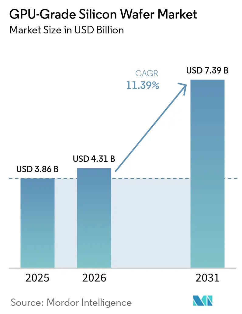
The GPU-grade silicon wafer market size is expected to expand from USD 3.86 billion in 2025 to USD 4.31 billion in 2026 and reach USD 7.39 billion by 2031, growing at an 18.85% CAGR from 2026 to 2031. Generative AI training clusters, the migration to 3 nm and 2 nm GPU architectures, and policy-driven onshoring incentives reshape substrate specifications and purchasing patterns. Polished prime wafers continue to dominate revenue, yet thicker epitaxial layers are becoming mandatory for backside power delivery networks, while large-area silicon-on-insulator (SOI) wafers underpin chiplet-based packaging. Pure-play foundries such as TSMC and Samsung Foundry lock in multi-year supply contracts to secure 300 mm capacity, leaving independent suppliers with shrinking spot volumes. Intensifying localization mandates in the United States and Europe, coupled with export controls on advanced node equipment, will fragment the global supply base and sharpen price differentiation between mainstream and premium substrates.
Key Report Takeaways
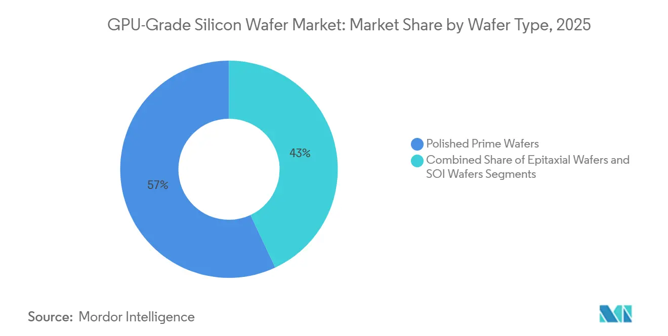
- By wafer type, polished prime substrates led with a 57% revenue share in 2025, whereas epitaxial wafers are advancing at an 11.99% CAGR through 2031.
- By process node, sub-7 nm designs captured 63% of 2025 shipments and are expanding at an 11.79% CAGR, reflecting the rapid ramp of NVIDIA Blackwell, AMD MI300, and forthcoming Intel Falcon Shores accelerators.
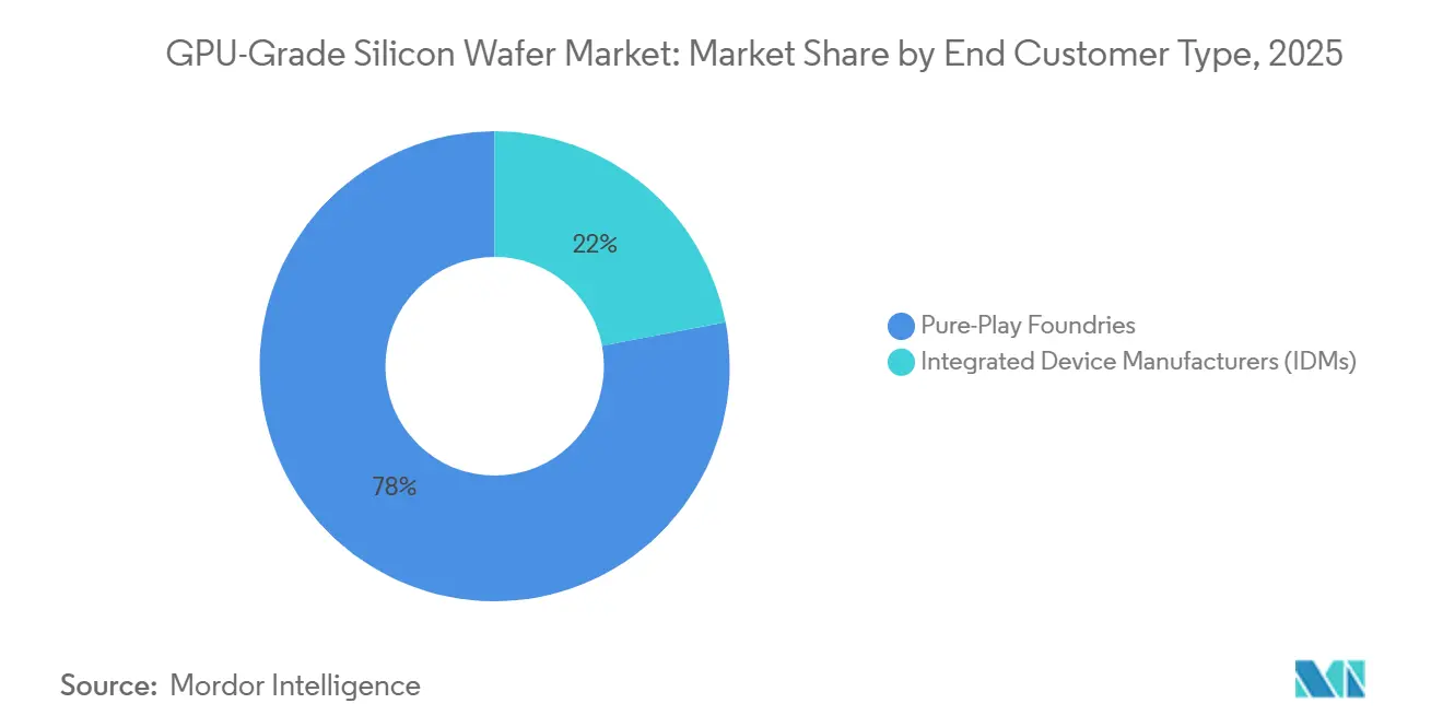
- By end-customer type, pure-play foundries accounted for 78% of 2025 volumes, while integrated device manufacturers are growing at a 11.83% CAGR as Intel and Samsung scale in-house GPU lines.
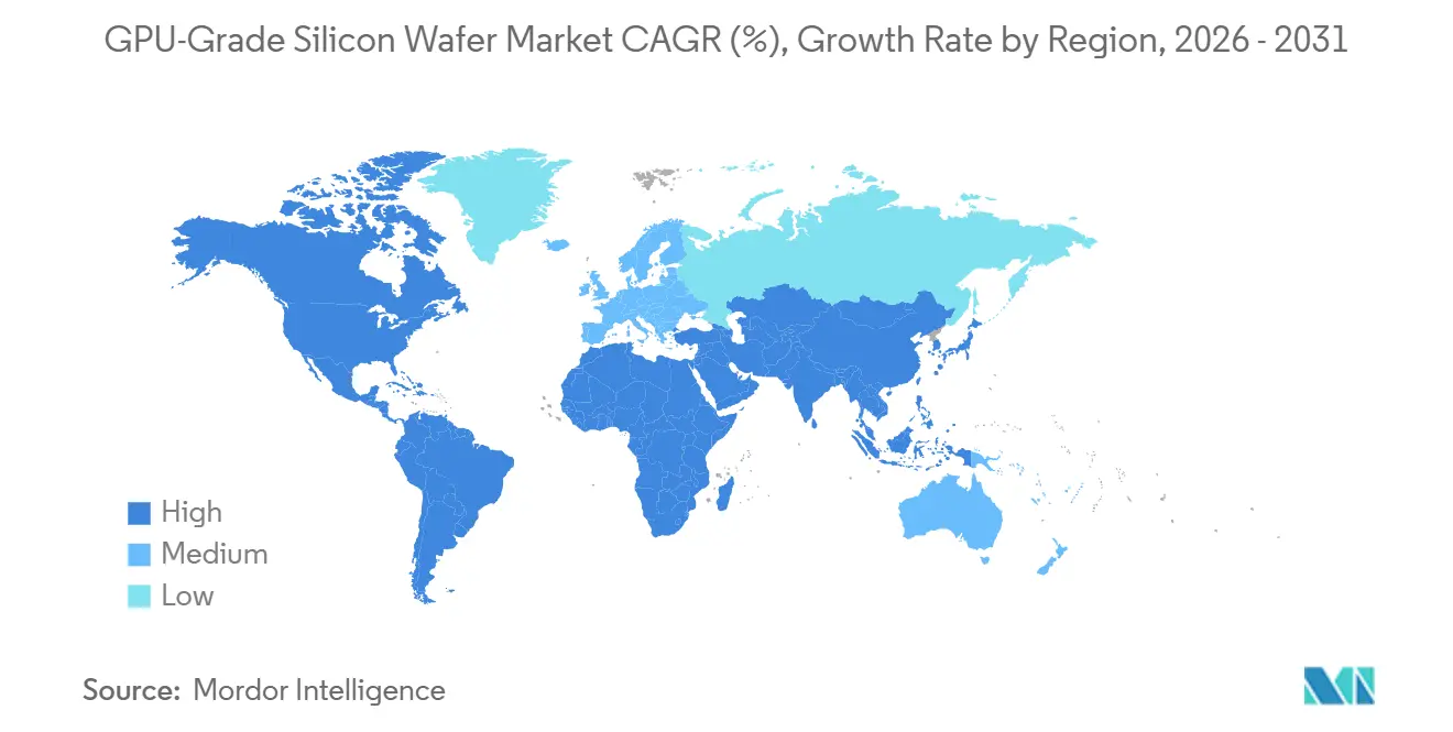
- By geography, Asia-Pacific accounted for 68% of 2025 demand, but North America is the fastest-growing region, with a 11.79% CAGR through 2031, driven by CHIPS Act-funded capacity.
Note: Market size and forecast figures in this report are generated using Mordor Intelligence’s proprietary estimation framework, updated with the latest available data and insights as of January 2026.
Market Trends and Insights
Drivers Impact Analysis of GPU-Grade Silicon Wafer Market*
| Driver | (~) % Impact on CAGR Forecast | Geographic Relevance | Impact Timeline |
|---|---|---|---|
| Exploding AI Training Compute Density Driving Ultra-Low Defect Requirements | +4.2% | Global, with concentration in North America and Asia-Pacific | Short term (≤ 2 years) |
| Rapid Ramp of 3 nm and 2 nm GPU Architectures Increasing 300 mm Prime Wafer Demand | +3.8% | Asia-Pacific core, spillover to North America and Europe | Medium term (2-4 years) |
| Shift Toward Backside Power Delivery Necessitating Thicker Epi Wafer Specs | +2.9% | Global, led by North America and Taiwan | Medium term (2-4 years) |
| Localization Incentives in U.S. and Europe for Strategic Wafer Supply | +2.5% | North America and Europe | Long term (≥ 4 years) |
| Emergence of Chiplet-Based GPU Designs Boosting Demand for Large-Area SOI Wafers | +1.8% | Global, with early adoption in North America and Asia-Pacific | Medium term (2-4 years) |
| Sustainability Mandates Driving Adoption of Reclaimed Prime Wafers for R&D | +0.6% | Europe and North America | Long term (≥ 4 years) |
| Source: Mordor Intelligence | |||
Exploding AI Training Compute Density Driving Ultra-Low Defect Requirements
GPU clusters now exceed 100,000 accelerators per installation, so a single wafer defect can cascade into millions of dollars in lost revenue. TSMC’s 3 nm N3E node requires defect densities below 0.09 defects/cm² to sustain yields above 70%. Shin-Etsu and SUMCO have therefore integrated advanced inline metrology that reduces scrap by 15% to 20% while polishing surface micro-roughness to sub-0.1 nm levels.[1] Tighter specifications prolong qualification cycles to as much as 9 months, but they also raise switching costs and reinforce supplier stickiness with the leading foundries.
Rapid Ramp of 3 nm and 2 nm GPU Architectures Increasing 300 mm Prime Wafer Demand
TSMC devoted about 40% of its 300 mm capacity to sub-5 nm nodes in 2025, equating to roughly 1.2 million wafer starts per month, while Samsung Foundry targets 50,000 wafer starts per month on its 3 nm gate-all-around line by late 2026. Node shrinkage, enlarged reticle sizes, and drive a 20%-30% uplift in wafer consumption per finished die. SUMCO responded by boosting its Japanese epi capacity 15% in 2025 to keep pace with AI accelerators. The jump to 2 nm in 2027-2028 will further tighten flatness and purity requirements, entrenching premium pricing for prime substrates.
Shift Toward Backside Power Delivery Necessitating Thicker Epi Wafer Specs
Intel’s PowerVia architecture moves power grids to the wafer backside, cutting voltage droop by 30% and demanding 10-15 µm epi layers versus the 3-5 µm used today. TSMC is on a parallel path for its 2 nm A16 node, so wafer suppliers are retrofitting reactors, which lift cycle times by 40% and push substrate prices up by 30%. Soitec is prototyping engineered SOI stacks that merge buried oxide with thick epi to support both backside power and chiplet bridges.
Localization Incentives in U.S. and Europe for Strategic Wafer Supply
The United States CHIPS and Science Act earmarked USD 52.7 billion for domestic semiconductor projects, with GlobalWafers securing a USD 400 million grant in January 2026 to build a 1.2 million-wafer-per-year plant in Texas. The European Union’s Chips Act allotted EUR 43 billion (USD 47.3 billion) in similar support, and Siltronic’s EUR 3.5 billion (USD 3.85 billion) Dresden fab will add another 1 million wafers annually from 2028. While these facilities take four to five years to ramp up, they are already dictating long-term procurement strategies that emphasize geographic redundancy.
Restraints Impact Analysis of GPU-Grade Silicon Wafer Market*
| Restraint | (~) % Impact on CAGR Forecast | Geographic Relevance | Impact Timeline |
|---|---|---|---|
| Limited High-Purity Polysilicon Supply Constraining 300 mm Output | -2.3% | Global, with acute impact in Asia-Pacific | Short term (≤ 2 years) |
| Long Qualification Cycles with GPU Customers Slowing Node Transitions | -1.9% | Global | Medium term (2-4 years) |
| Capital Intensity of Float-Zone 300 mm Lines Deterring New Entrants | -1.2% | Global | Long term (≥ 4 years) |
| Trade Restrictions on Advanced Node Equipment Limiting Expansion in China | -1.0% | China, with spillover to global supply | Medium term (2-4 years) |
| Source: Mordor Intelligence | |||
Limited High-Purity Polysilicon Supply Constraining 300 mm Output
Only Hemlock Semiconductor, Wacker Chemie, and OCI consistently achieve 11-nines purity, and combined semiconductor-grade output of roughly 180,000 t yr-¹ in 2025 fell short of the 200,000 t yr-¹ required for wafers and solar cells.[2] Lead times for new orders stretched to 40 weeks at Wacker’s Burghausen facility, prompting wafer vendors to ration allocations toward long-term contracts. Hemlock’s USD 250 million Tennessee expansion will add 10,000 t yr-¹ by 2027, but barely covers incremental demand from U.S. CHIPS Act fabs.
Long Qualification Cycles with GPU Customers Slowing Node Transitions
Advanced GPU nodes require 18-24 months of wafer qualification, including pilot-line test runs, high-volume correlation, and reliability screening. TSMC’s 3 nm protocol alone spans nine months of metrology and stress testing. Foundries, therefore, resist dual-sourcing critical substrates, which leaves emerging suppliers locked out and constrains the flexibility of capacity reallocation. Epitaxial wafers face the steepest hurdles because dopant uniformity and layer flatness must be validated across millions of wafer starts.
*Our forecasts treat driver/restraint impacts as directional, not additive. The impact forecasts reflect baseline growth, mix effects, and variable interactions.
GPU-Grade Silicon Wafer Market Segment Analysis
By Wafer Type:
Thicker Epi Layers Gain TractionEpitaxial substrates are experiencing the fastest growth, with a CAGR of 11.99% projected through 2031. This growth is driven by the increasing demand for backside power delivery and through-silicon vias, which require 10-15 µm epi thicknesses that polished prime wafers cannot support. In 2025, polished prime wafers accounted for 57% of revenue, ensuring the GPU-grade silicon wafer market for mainstream nodes remains significant. However, this dominance is expected to decline as nodes of 3 nm and below enter mass production. Intel’s PowerVia roadmap highlights this transition, with its 18A designs relying heavily on epitaxial surfaces capable of handling aggressive via aspect ratios.
The market share of SOI substrates within the GPU-grade silicon wafer market, although relatively small in 2025, is steadily increasing. This growth is attributed to the reliance of chiplet layouts on low-capacitance interposers. Soitec’s Smart Cut technology plays a pivotal role in this trend by depositing a 20 nm buried oxide layer beneath a 6 nm active layer, facilitating heterogeneous stacking while reducing thermal resistance. Despite cost pressures making polished prime wafers more appealing for nodes of 7 nm and above, the superior yields and power efficiency at the leading edge continue to drive investments in epitaxial substrates.

By Process Node:
Sub-7 nm Commands Two-Thirds of RevenueNodes finer than 7 nm are projected to capture 63% of the demand in 2025, driven by an impressive compound annual growth rate (CAGR) of 11.79%. This growth aligns with GPU roadmaps that aim to integrate hundreds of billions of transistors per die, showcasing the increasing complexity and performance of these technologies. TSMC’s N3E process alone is anticipated to consume approximately 400,000 wafers per month in 2025, with allocations evenly split between Apple and AI accelerator customers, reflecting the strong demand from these key sectors. Meanwhile, Samsung’s 3 nm gate-all-around technology is expected to ramp up production to achieve similar volumes by late 2026, further intensifying competition in the advanced node market.
Nodes ranging from 7 nm to 14 nm are emerging as a cost-effective platform, particularly for applications such as automotive infotainment systems and edge AI solutions, where the economics of 5 nm nodes remain challenging. GlobalFoundries is actively expanding its 12 nm FinFET production lines in New York and Singapore, leveraging incentives provided by the CHIPS Act to support this growth. The GPU-grade silicon wafer market, which is closely tied to advanced but not cutting-edge nodes, continues to demonstrate resilience. However, the price gap between premium and standard substrates is widening as yield thresholds for leading-edge technologies become increasingly stringent, adding complexity to the supply chain dynamics.
By End Customer Type:
Foundries Retain Purchasing PowerPure-play foundries absorbed 78% of shipments in 2025, leveraging their significant volume to negotiate take-or-pay supply contracts that extend through 2028. These contracts provide stability and predictability in supply chains, ensuring consistent wafer availability for key customers. TSMC secured approximately 60% of its 2026 wafer requirements through agreements signed during 2024-2025, with a strong focus on fulfilling the demands of major clients such as Apple, NVIDIA, and AMD. Similarly, Samsung Foundry entered into a three-year agreement with SK Siltron, ensuring a steady supply of 150,000 wafers per month starting from mid-2026. These strategic partnerships highlight the importance of long-term planning and collaboration in maintaining a competitive edge in the market.
Integrated device manufacturers (IDMs) are experiencing the fastest growth, with a compound annual growth rate (CAGR) of 11.83%, as Intel Foundry Services and Samsung’s in-house Exynos program scale up production. These IDMs are actively diversifying their sourcing strategies to mitigate risks associated with spot pricing fluctuations. For instance, Intel has signed letters of intent to procure Domestic-content-compliant wafers from GlobalWafers’ upcoming Texas facility, which is expected to enhance supply chain resilience. This evolving landscape in the GPU-grade silicon wafer industry increasingly favors vertically integrated buyers who can leverage their volume commitments to negotiate price concessions ranging from 15% to 20%, thereby optimizing their cost structures while ensuring a reliable supply of critical materials.
Geography Analysis
APAC GPU-Grade Silicon Wafer Market
Asia-Pacific controlled 68% of 2025 revenue thanks to TSMC’s Hsinchu and Tainan megafabs alongside Samsung’s Hwaseong and Pyeongtaek complexes, which together ran about 2.5 million 300 mm wafers per month for leading-edge GPUs. Japan and South Korea, home to Shin-Etsu, SUMCO, and SK Siltron, supplied roughly 55% of global substrate output, underscoring the region’s depth across the value chain. China accounted for 12%-15% of consumption but faces an effective ceiling after December 2024, when export controls blocked ASML deep-ultraviolet tools, capping domestic 7 nm capability.[3]
North America GPU-Grade Silicon Wafer Market
North America is the fastest-growing region, with a 11.79% CAGR through 2031. CHIPS Act grants of USD 52.7 billion, led by the USD 400 million award to GlobalWafers, will add 1.2 million wafers per year in Texas from 2028. Intel’s Foundry Services expansions in Arizona, New Mexico, and Ohio, plus hyperscaler demand for sovereign AI capacity, funnel steady offtake into domestic plants. The GPU-grade silicon wafer market in North America could double by 2031 if scheduled fabs come online as planned.
EMEA, APAC and South America GPU-Grade Silicon Wafer Market
Europe captured 8% of 2025 revenue, clustered in Germany’s Saxony region where Infineon, Bosch, and GlobalFoundries operate mature-node lines. Siltronic’s EUR 3.5 billion (USD 3.85 billion) Dresden investment, underwritten by EUR 1.2 billion (USD 1.32 billion) in EU Chips Act grants, is set to lift the continent’s share to roughly 12%-14% by 2031. Middle East and Africa together with South America remain minor, at under 2% combined, while India’s incentive program has yet to translate into shovel-ready wafer projects.
Competitive Landscape
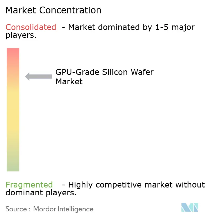
The GPU-grade silicon wafer market remains highly concentrated. Shin-Etsu, SUMCO, and Siltronic jointly controlled about 65% of the 300 mm capacity in 2025, a structure that supports premium pricing and controlled allocation strategies. Shin-Etsu posted JPY 2,561.2 billion (USD 17.1 billion) in fiscal-2025 revenue, with semiconductor silicon offsetting softness in legacy nodes. Investment focuses on shortening qualification cycles, with Shin-Etsu opening a JPY 15 billion (USD 100 million) EUV photoresist plant in April 2026 that bundles substrates and resists for 2 nm processes.
Vertical integration reshapes rivalry. Samsung’s strategic stake in SK Siltron secures 150,000 wafers per month of priority supply beginning July 2026, while Intel angles for volume from GlobalWafers’ Texas fab to guarantee U.S. content compliance. Smaller challengers leverage niche innovations, Soitec exploits Smart Cut for SOI chiplet substrates and targets gate-all-around nanosheet nodes in partnership with imec. Chinese entrants Shanghai Silicon Industry and Zhonghuan Semiconductor expand 300 mm capacity for 14 nm and larger nodes despite tool embargoes, relying on CNY 13.2 billion (USD 1.85 billion) in state aid.[4]
Technology differentiation is becoming increasingly significant, focusing on float-zone Czochralski hybrids that enhance resistivity for high-performance computing applications. Additionally, reclaimed wafer programs are gaining traction, as they reduce embodied carbon emissions by approximately 40%, contributing to sustainability goals. Automation advancements are also playing a critical role, reducing cycle times by 20% and improving overall efficiency in production processes. Established players in the market leverage their scale advantages in research and development (R&D) and capital investments to maintain their competitive edge. However, policy-driven diversification efforts are gradually impacting their market share, as new regional fabrication facilities (fabs) are being established to support localized production and reduce dependency on existing supply chains.
GPU-Grade Silicon Wafer Industry Leaders
-
Shin-Etsu Handotai Co., Ltd.
-
SUMCO Corporation
-
GlobalWafers Co., Ltd.
-
Siltronic AG
-
SK Siltron Co., Ltd.
- *Disclaimer: Major Players sorted in no particular order
GPU-Grade Silicon Wafer Market Companies Covered in this Report
- Shin-Etsu Handotai Co., Ltd.
- SUMCO Corporation
- Siltronic AG
- GlobalWafers Co., Ltd.
- SK Siltron Co., Ltd.
- Wafer Works Corp.
- Soitec S.A.
- Shanghai Simgui Technology Co., Ltd.
- Okmetic Oyj
- Ferrotec Holdings Corporation
- Hangzhou Silicon Tech Co., Ltd. (HJSemi)
- Zhonghuan Semiconductor Co., Ltd.
- POSCO Future M Co., Ltd.
- Episil-Precision Inc.
- MEMC Korea Company
- Korea Silicon Wafer Co., Ltd.
- Linton Crystal Technologies
- Salem Advanced Materials Inc.
- Noel Technologies
- Topsil GlobalWafers
Recent Industry Developments in GPU-Grade Silicon Wafer Market
- April 2026: Shin-Etsu Handotai started operations at a JPY 15 billion (USD 100 million) EUV photoresist facility in Isesaki, Japan, to supply bundled resist and wafer solutions for 2 nm production.
- March 2026: SK Siltron secured KRW 500 billion (USD 358 million) from South Korea’s National Growth Fund to accelerate a new 300 mm plant in Gumi, slated for July 2026 start-up.
- January 2026: GlobalWafers received a USD 400 million CHIPS Act grant to build a USD 5 billion, 1.2 million-wafer-a-year fab in Sherman, Texas, with production targeted for 2028.
- November 2025: Soitec and imec launched a EUR 50 million (USD 55 million) program to co-develop fully depleted SOI substrates for 2 nm gate-all-around GPUs.
Global GPU-Grade Silicon Wafer Market Report Scope
The GPU-grade silicon wafer market is the global industry that produces, supplies, and commercializes high-purity silicon wafers specifically engineered for the fabrication of graphics processing units (GPUs). These wafers serve as the foundational substrate upon which advanced semiconductor devices are built, enabling the high computational performance required for applications such as artificial intelligence (AI), machine learning (ML), high-performance computing (HPC), and data center acceleration.
The GPU-Grade Silicon Wafer Market Report is Segmented by Wafer Type (Polished Prime Wafers, Epitaxial Wafers, and SOI Wafers), Process Node (Leading Edge Nodes below 7 nm, and Advanced Nodes 7-14 nm), End Customer Type (Pure-Play Foundries, and IDMs), and Geography (North America, Europe, Asia-Pacific, and Rest of the World). Market Forecasts are Provided in Terms of Value (USD).
Segmentation Overview
| Polished Prime Wafers |
| Epitaxial (Epi) Wafers |
| SOI (Silicon-on-Insulator) Wafers |
| Leading Edge Nodes (<7 nm) |
| Advanced Nodes (7-14 nm) |
| Pure-Play Foundries |
| Integrated Device Manufacturers (IDMs) |
| North America | United States |
| Canada | |
| Mexico | |
| Europe | United Kingdom |
| Germany | |
| Rest of Europe | |
| Asia-Pacific | China |
| Japan | |
| India | |
| South Korea | |
| Rest of Asia-Pacific | |
| Rest of the World |
| By Wafer Type | Polished Prime Wafers | |
| Epitaxial (Epi) Wafers | ||
| SOI (Silicon-on-Insulator) Wafers | ||
| By Process Node | Leading Edge Nodes (<7 nm) | |
| Advanced Nodes (7-14 nm) | ||
| By End Customer Type | Pure-Play Foundries | |
| Integrated Device Manufacturers (IDMs) | ||
| By Geography | North America | United States |
| Canada | ||
| Mexico | ||
| Europe | United Kingdom | |
| Germany | ||
| Rest of Europe | ||
| Asia-Pacific | China | |
| Japan | ||
| India | ||
| South Korea | ||
| Rest of Asia-Pacific | ||
| Rest of the World | ||
Key Questions Answered in the Report
What is the current GPU-grade silicon wafer market size?
The GPU-grade silicon wafer market size reached USD 4.31 billion in 2026 and is projected to hit USD 7.39 billion by 2031.
Which wafer type is growing fastest for GPUs?
Epitaxial substrates lead growth at an 11.99% CAGR through 2031 because thicker epi layers are critical for backside power delivery designs.
How will CHIPS Act funding affect regional supply?
CHIPS Act grants, such as the USD 400 million award to GlobalWafers, will add 1.2 million wafers per year in Texas by 2028, lifting North America's global share from 32% in 2025 to roughly 40% by 2031.
Why are sub-7 nm nodes consuming most wafers?
GPUs built on 3 nm and 2 nm nodes pack more transistors per die, expand reticle sizes, and require redundancy, raising wafer starts by 20%-30% compared with 7 nm designs.
Who controls the bulk of 300 mm wafer capacity?
Shin-Etsu Handotai, SUMCO, and Siltronic command around 65% of global capacity, giving them leverage to set pricing and allocate supply during shortages.
What is the main supply-side bottleneck today?
Semiconductor-grade polysilicon purity remains constrained, with demand outstripping the 180,000 t yr-¹ available in 2025, extending lead times to as long as 40 weeks.