GaN Substrate Market Size and Share
Market Overview
| Study Period | 2020 - 2031 |
|---|---|
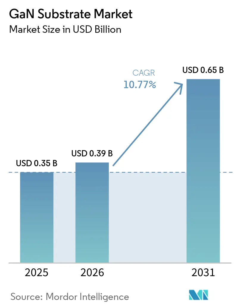
| Market Size (2026) | USD 0.39 Billion |
| Market Size (2031) | USD 0.65 Billion |
| Growth Rate (2026 - 2031) | 10.77% CAGR |
| Fastest Growing Market | Middle East |
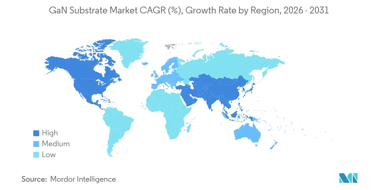
| Largest Market | Asia Pacific |
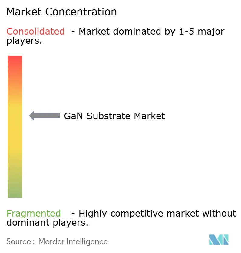
| Market Concentration | Medium |
Major Players *Disclaimer: Major Players sorted in no particular order Image © Mordor Intelligence. Reuse requires attribution under CC BY 4.0. | |
GaN Substrate Market Analysis by Mordor Intelligence
The GaN substrate market size is expected to increase from USD 0.35 billion in 2025 to USD 0.39 billion in 2026 and reach USD 0.65 billion by 2031, growing at a CAGR of 10.77% over 2026-2031. The uptrend rests on GaN’s high electron mobility and thermal conductivity, qualities that are indispensable for next-generation power conversion, radio-frequency amplification, and micro-LED backplanes. Automotive electrification continues to demand higher power density in on-board chargers, 5G and soon-to-launch 6G infrastructure relies on GaN-on-SiC power amplifiers, and display makers are scaling native GaN wafers to meet low-defect thresholds for sub-10-micrometer pixels. Supply volatility in gallium, intensifying geopolitical competition for wide-bandgap materials, and steady cost-out innovations in hydride vapor-phase epitaxy all play pivotal roles in shaping the growth path of the GaN substrate market.
Key Report Takeaways
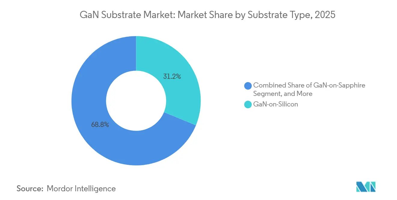
- By substrate type, GaN-on-silicon captured 31.19% of the GaN substrate market size in 2025, whereas GaN-on-diamond is forecast to grow at 11.24% CAGR.
- By wafer size, 6-inch wafers accounted for 42.82% of the GaN substrate market in 2025; the 8-inch-and-above segment is poised to expand at a 11.51% CAGR.
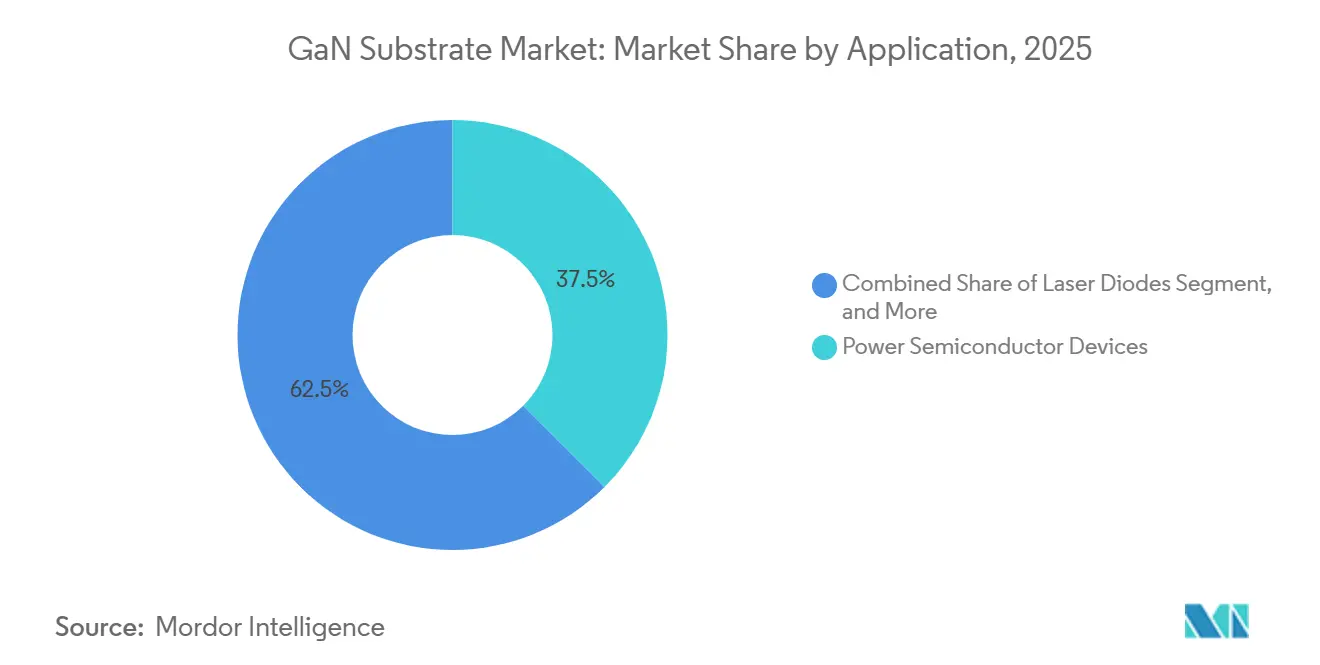
- By application, power semiconductor devices led with 37.49% of the GaN substrate market share in 2025, while RF devices are poised for an 11.38% CAGR through 2031.
- By end-use industry, telecommunications and data centers held 29.25% share in 2025; automotive and transportation are set to register an 11.18% CAGR to 2031.
- By geography, Asia-Pacific led with 41.33% GaN substrate market share in 2025, while the Middle East is projected to advance at an 11.33% CAGR through 2031.
Note: Market size and forecast figures in this report are generated using Mordor Intelligence’s proprietary estimation framework, updated with the latest available data and insights as of January 2026.
Global GaN Substrate Market Trends and Insights
Driver Impact Analysis*
| Driver | (~) % Impact on CAGR Forecast | Geographic Relevance | Impact Timeline |
|---|---|---|---|
| Rising Adoption in EV On-Board Fast-Charging Systems | +2.5% | Global, with early commercial traction in China and Europe | Medium term (2-4 years) |
| Surging Micro-LED Display Production Requiring Low-Defect Native GaN Wafers | +2% | Asia-Pacific core, spillover to North America | Medium term (2-4 years) |
| Telecom 5G/6G PA Build-Out Accelerating Demand for High-Thermal-Conductivity GaN-on-SiC Substrates | +1.8% | Global, led by North America defense and Asia-Pacific commercial infrastructure | Short term (≤ 2 years) |
| Rapid Scale-Up of 6-Inch HVPE Free-Standing GaN Production Lowering Cost per cm² | +1.5% | Japan and China manufacturing hubs, global supply impact | Medium term (2-4 years) |
| Government-Funded Wafer-Reuse (Laser-Slicing) Programs Slashing Substrate Cost by >40% | +1.0% | Japan, United States, with technology transfer to Europe | Long term (≥ 4 years) |
| Venture Investment in Diamond-Integrated GaN Substrates for Extreme Power Density | +0.8% | North America and Japan R&D, niche defense and satellite applications | Long term (≥ 4 years) |
| Source: Mordor Intelligence | |||
Rising Adoption in EV On-Board Fast-Charging Systems
Electric-vehicle makers now specify GaN‐based on-board chargers that hit 96% efficiency and 6 kW L⁻¹ power density, results validated when Changan deployed Navitas GaNSafe devices in 2025. Subsequent 6.6 kW units from Inovance Automotive delivered 30% higher power density than silicon IGBTs and trimmed charger weight by 20%. Infineon’s automotive-qualified 100 V GaN transistors cleared AEC-Q101 later in 2025, confirming that qualification hurdles have been overcome. Demand curves point to more than 1 million GaN chargers per year by 2028, a volume that motivates substrate suppliers to transition from 6-inch to 8-inch platforms. Native GaN and GaN-on-SiC suppliers, therefore, face a window to lock in long-term supply contracts with Tier-1 automotive integrators.
Surging Micro-LED Display Production Requiring Low-Defect Native GaN Wafers
Micro-LED fabs impose dislocation density ceilings of 10⁴ cm⁻², a level unreachable on GaN-on-sapphire. Hybrid ammonothermal and HVPE growth schemes now deliver free-standing GaN wafers that meet that threshold, enabling wafer-scale mass transfer of micro-LED arrays onto CMOS backplanes. Mitsubishi Chemical demonstrated 4-inch crystals under a NEDO program in 2025, aiming at 1 000 wafers per month and enabling panel luminance beyond 100 000 nits for outdoor augmented-reality headsets. Display houses are simultaneously refining sidewall passivation chemistries to keep non-radiative recombination in check, ensuring that substrate quality propagates to final brightness performance.
Telecom 5G/6G PA Build-Out Accelerating Demand for High-Thermal-Conductivity GaN-on-SiC Substrates
Millimeter-wave base-station amplifiers push heat flux above 30 W mm⁻², conditions that only GaN-on-SiC, with 490 W m⁻¹ K⁻¹ thermal conductivity, can manage reliably. Qorvo’s QPA1722 entered volume production in 2025, delivering 10 W of saturated power across K-band with 36% power-added efficiency. Mitsubishi Electric has verified GaN PAs that comply with 3GPP Release 18 carrier-aggregation rules, a milestone that unlocks multi-band massive-MIMO designs for 5G-Advanced. Defense prime contractors continue to reserve GaN-on-SiC for AESA radar and electronic warfare, intensifying substrate demand at the very moment commercial telecom ramps.
Rapid Scale-Up of 6-Inch HVPE Free-Standing GaN Production Lowering Cost per cm²
HVPE achieves GaN growth rates ten times faster than MOCVD, supporting thick-boule production that lifts off from sacrificial templates. Sumitomo Chemical, backed by NEDO, targets threading-dislocation densities below 10⁵ cm⁻² on 6-inch wafers while keeping crack formation in check. Shin-Etsu’s QST composite platform extends the concept to 300 mm, marrying GaN with silicon toolsets and trimming substrate cost per die by an expected 40% once volumes scale. Polishing still drags throughput because GaN’s Vickers hardness reaches 2 000, yet slurry innovation and pad design are steadily lifting material-removal rates.
Restraints Impact Analysis*
| Restraint | (~) % Impact on CAGR Forecast | Geographic Relevance | Impact Timeline |
|---|---|---|---|
| High Wafer Price Premium Versus Si and SiC Limiting Adoption in Cost-Sensitive Segments | -1.5% | Global, most acute in consumer electronics and industrial power | Short term (≤ 2 years) |
| Device-Yield Losses from Threading-Dislocation Clusters on 6-Inch Wafers | -1.2% | Asia-Pacific and North America manufacturing hubs | Medium term (2-4 years) |
| Supply-Chain Choke-Points in HVPE/Ammonothermal Equipment and Chlorine Gas | -0.8% | Global, concentrated in Japan and Europe equipment suppliers | Medium term (2-4 years) |
| Geopolitical Export-Control Risks on Gallium Feedstock After 2024 China Restrictions | -0.6% | Non-China regions dependent on Chinese gallium, spillover to global pricing | Short term (≤ 2 years) |
| Source: Mordor Intelligence | |||
High Wafer Price Premium Versus Si and SiC Limiting Adoption in Cost-Sensitive Segments
Native GaN and GaN-on-SiC wafers still command USD 3 000-8 000 per 6-inch unit, five to ten times the tag on comparable silicon carbide wafers. Consumer and industrial designers therefore stick with silicon IGBTs or SiC MOSFETs, sacrificing modest efficiency gains to avoid heavy bill-of-materials penalties. Ammonothermal growth produces superb crystal quality but requires 3 000-bar autoclaves running for weeks, tying up capital and capping throughput. Laser-based wafer-reuse projects at Nagoya University demonstrate up to 10 recycles without degrading device metrics, yet commercial cycle times have not yet matched the cadence of conventional foundry flows.
Device-Yield Losses from Threading-Dislocation Clusters on 6-Inch Wafers
Dislocations propagate vertically and create leakage channels that shrink breakdown voltage and shorten device lifetime. Six-inch HVPE or ammonothermal wafers often achieve densities of 10⁴-10⁶ cm⁻², leading to yield losses above 20% in 650 V transistors. Edge exclusion zones subtract another 10-15% of usable die area, inflating effective substrate cost. Mitsubishi Chemical’s hybrid sodium-flux method cut dislocation density below 10⁴ cm⁻² on 4-inch samples, but scaling that precision to 8-inch demands perfect control of thermal gradients and nutrient transport, an unresolved hurdle.
*Our forecasts treat driver/restraint impacts as directional, not additive. The impact forecasts reflect baseline growth, mix effects, and variable interactions.
Segment Analysis
By Substrate Type: Native GaN Drives Premium ApplicationsBy Substrate Type: GaN-on-Silicon Leads as Diamond Integration Gains Speed
GaN-on-silicon held 31.19% of the GaN substrate market share in 2025, thanks to a seamless fit with 200 mm fabs and a sub-USD 200 cost per wafer. Innoscience ramped 8-inch lines from 13 000 to 20 000 wafers per month and targets 70 000 by 2030, underlining China’s capacity lead. The GaN substrate market size for diamond-integrated variants is projected to grow at 11.24% CAGR through 2031 as bonding lowers thermal resistance below 10 mm² K W⁻¹ and enables power densities above 30 W mm⁻² for phased-array radar.
Legacy GaN-on-sapphire maintains a foothold in general lighting, but share erodes as micro-LED and RF segments pivot to native GaN for defect control. GaN-on-SiC stays indispensable for high-heat telecom and defense systems, with Qorvo and Wolfspeed the default suppliers. Native GaN, though pricier, secures ultra-low dislocation counts for vertical power transistors and fine-pitch display backplanes, and Shin-Etsu’s 300 mm QST composite route may bridge cost and quality gaps over the forecast horizon.


By Wafer Size: 6-Inch Dominates While 8-Inch Transition Accelerates
Six-inch inventory represented 42.82% of the GaN substrate market size in 2025 as HVPE reactors and CMP tools are fully depreciated at that diameter. This dominance is attributed to the maturity of six-inch manufacturing processes, which have achieved cost efficiency and scalability. Sumitomo Chemical’s NEDO-backed line uses 100-300 µm h⁻¹ deposition rates to keep cycle times competitive and pull defect density below 10⁵ cm⁻², ensuring high-quality substrates suitable for various applications. The 8-inch-and-above cohort is on track for 11.51% CAGR to 2031, catalyzed by Infineon’s announcement of 300 mm GaN lines and Chinese IDMs mapping 70 000 wafers per month by 2030.
This growth is driven by increasing demand for larger substrates to support high-power, high-frequency applications, as well as advancements in manufacturing technologies. A proof-of-concept 8-inch free-standing GaN was demonstrated in early 2026, yet cracking and CMP time remain stumbling blocks, highlighting the challenges in scaling up production. Two- and four-inch wafers persist in R&D and niche RF applications, where smaller substrates are sufficient for specialized use cases. Meanwhile, 300 mm composite substrates position GaN for mainstream silicon fabs once economics tighten, paving the way for broader adoption in the semiconductor industry.
By Application: Power Devices Command Share, RF Surges as Fastest Riser
Power semiconductors accounted for 37.49% of the GaN substrate market share in 2025, driven by their application in EV on-board chargers, 48 V DC-DC converters, and industrial drives. These semiconductors have become a critical component in enabling higher efficiency and compact designs in power electronics. Navitas GaNSafe parts, featured in the Changan Qiyuan E07, demonstrated an impressive 96% efficiency and power density, unmatched by traditional silicon-based solutions. Looking ahead, Renesas bidirectional GaN switches are expected to expand their application into energy-storage inverters, signaling the potential for a more diverse and advanced device portfolio in the coming years.
RF devices are projected to be the primary growth driver, with an anticipated CAGR of 11.38% through 2031. This growth is fueled by increasing demand for K-band satellite payloads, 5G-Advanced macro cells, and defense radar systems, all of which require high-performance specifications, such as a saturated power of 10 W and a power-added efficiency (PAE) exceeding 35%. While the LED segment is experiencing a decline in market share due to the maturity of solid-state lighting applications, laser diodes and emerging quantum sensors are carving out smaller but strategically significant niches.
By End-Use Industry: Telecom Holds Lead, Automotive Poised for Overtake
Telecommunications and data centers accounted for 29.25% of the GaN substrate market in 2025, primarily driven by the increasing adoption of GaN-on-SiC power amplifiers (PAs) in 5G radios and GaN DC-DC bricks in server racks. The demand for higher efficiency and power density in these applications has positioned GaN substrates as a critical component in the telecommunications and data center sectors. Additionally, defense RF GaN projects have shown steady growth, although they operate within capped procurement cycles due to budgetary constraints and specific project requirements.
Automotive and transportation, projected to grow at a CAGR of 11.18%, is expected to surpass the telecommunications sector before 2029. This growth is fueled by the widespread adoption of GaN technology in mass-market electric vehicle (EV) programs, particularly in on-board chargers and traction inverters, which require high efficiency and compact designs. However, the consumer electronics segment faces challenges due to tight profit margins, which have slowed the adoption of GaN technology. Significant cost reductions, such as those achieved through wafer reuse, are anticipated to drive future growth in this segment. Meanwhile, the industrial, aerospace, and healthcare sectors account for the remaining demand for GaN substrates, focusing on specialized, often ruggedized GaN devices tailored to meet the unique requirements of these industries.
Geography Analysis
Asia-Pacific accounted for 41.33% of the GaN substrate market share in 2025. Chinese IDMs, supported by domestic capital investments and abundant gallium feedstock, continue to expand their 8-inch GaN-on-silicon production lines to meet growing demand. Japan, on the other hand, capitalizes on its advanced crystal growth expertise to produce free-standing native GaN substrates and to explore emerging diamond-bonded technologies. South Korea’s display manufacturers are increasingly relying on native GaN substrates to advance their micro-LED technology roadmaps, while India’s AGNIT Semiconductors is scaling up production under favorable tax incentives and government support programs.
North America combines its strong design leadership with increasing defense-related demand for GaN-on-SiC substrates. However, the region faces limitations in domestic substrate production capacity, currently limited to Kyma Technologies and small-scale university fabrication facilities. Europe’s competitive edge lies in Belgium’s Soitec EpiGaN unit, which plays a pivotal role in GaN substrate production across the region. Additionally, the European Union Chips Act provides significant funding aimed at achieving self-sufficiency in wide-bandgap semiconductor technologies.
The Middle East is emerging as the fastest-growing region, with a projected CAGR of 11.33% through 2031. Sovereign wealth funds in the region are actively stockpiling gallium and financing the establishment of greenfield substrate fabrication facilities. These efforts align with broader initiatives to support AI data centers and defense modernization programs. South America and Africa, while still in the early stages of development, hold potential for unlocking renewable energy-related GaN demand by the end of the decade. This growth is contingent on the establishment of regional fabrication capabilities to support local markets.

Competitive Landscape
Japanese chemical majors, including Sumitomo Electric, Mitsubishi Chemical, and Shin-Etsu Chemical, and Chinese IDMs such as San’an Semiconductor and Innoscience, collectively hold roughly 60% of installed capacity. However, fragmentation across substrate types prevents individual companies from capturing more than 15% of the market. The export curbs on gallium imposed by China in late 2024 have triggered a global scramble for alternative feedstock sources, particularly from Canada and Kazakhstan. This situation has compelled non-Chinese firms to pursue vertical integration, encompassing both upstream refining and downstream epitaxy, to stabilize their profit margins and ensure supply chain resilience.
Three competitive vectors currently dominate the market landscape. The first involves scaling HVPE (Hydride Vapor Phase Epitaxy) processes to achieve deposition rates of 300 µm h⁻¹ while maintaining defect densities below 10⁵ cm⁻². The second focuses on reducing CMP (Chemical-Mechanical Polishing) time by using specialized slurries designed to address GaN’s high hardness of 2,000 Vickers. The third vector emphasizes validating five-to-ten wafer-reuse cycles without compromising electrical performance,therebyd significantlyreducinge production costs. Wolfspeed’s strategic shift into GaN-on-SiC epitaxy, following its success with 300 mm SiC wafers, signals a convergence of SiC and GaN roadmaps. This development is expected to intensify cross-material competition, particularly in automotive applications where performance and efficiency are critical.
Disruptors in the market include startups specializing in diamond integration, which aim to push the boundaries of power density, and Indian manufacturers leveraging state-sponsored incentives to localize production and reduce dependency on imports. The growing importance of intellectual property in areas such as diamond bonding, laser lift-off techniques, and autoclave design is increasingly distinguishing leading players from the rest of the market. These advancements are reinforcing a moderately concentrated yet technologically dynamic GaN substrate market, where innovation continues to drive competitive differentiation.
GaN Substrate Industry Leaders
Sumitomo Electric Industries, Ltd.
Mitsubishi Chemical Corporation
Wolfspeed, Inc.
Shin-Etsu Chemical Co., Ltd.
SCIOCS Company, Ltd.
- *Disclaimer: Major Players sorted in no particular order

Recent Industry Developments
- March 2026: Renesas added 650 V bidirectional GaN switches for AI infrastructure and solar inverters, extending its GaN catalog.
- March 2026: AGNIT Semiconductors raised USD 2.6 million seed extension funding to scale GaN production to 100 000 parts in 24 months.
- January 2026: Wolfspeed reported the first 300 mm silicon carbide wafers, aiming to cut the cost per die for devices positioned against GaN solutions.
- January 2026: South Korea launched grants to commercialize 6-inch and 8-inch GaN power processes, bolstering domestic supply chains.


Global GaN Substrate Market Report Scope
The gallium nitride (GaN) substrate market is the global industry that produces, develops, and commercializes GaN-based substrate materials used as foundational layers for high-performance semiconductor devices. GaN substrates enable superior electrical, thermal, and optical properties compared to traditional materials, making them essential for applications requiring high efficiency, high power density, and high-frequency operation.
The GaN Substrate Market Report is Segmented by Substrate Type (GaN-on-Sapphire, GaN-on-Silicon, GaN-on-Silicon Carbide, Native GaN, and GaN-on-Diamond), Wafer Size (2 Inch, 4 Inch, 6 Inch, and 8 Inch and Above), Application (LEDs, Laser Diodes, Power Semiconductor Devices, RF Devices, and Other Applications), End-Use Industry (Consumer Electronics, Automotive and Transportation, Telecommunications and Data Centers, Industrial and Power, Aerospace and Defense, and Healthcare and Life Sciences), and Geography (North America, South America, Europe, Asia-Pacific, Middle East, and Africa). Market Forecasts are Provided in Terms of Value (USD).
| GaN-on-Sapphire |
| GaN-on-Silicon |
| GaN-on-Silicon Carbide |
| Native GaN (GaN-on-GaN) |
| GaN-on-Diamond |
| 2 Inch |
| 4 Inch |
| 6 Inch |
| 8 Inch and Above |
| Light-Emitting Diodes (LEDs) |
| Laser Diodes |
| Power Semiconductor Devices |
| Radio-Frequency Devices |
| Other Applications |
| Consumer Electronics |
| Automotive and Transportation |
| Telecommunications and Data Centers |
| Industrial and Power |
| Aerospace and Defense |
| Healthcare and Life Sciences |
| North America | United States |
| Canada | |
| Mexico | |
| South America | Brazil |
| Argentina | |
| Rest of South America | |
| Europe | Germany |
| United Kingdom | |
| France | |
| Russia | |
| Rest of Europe | |
| Asia-Pacific | China |
| Japan | |
| India | |
| South Korea | |
| Australia | |
| Rest of Asia-Pacific | |
| Middle East | Saudi Arabia |
| United Arab Emirates | |
| Rest of Middle East | |
| Africa | South Africa |
| Egypt | |
| Rest of Africa |
| By Substrate Type | GaN-on-Sapphire | |
| GaN-on-Silicon | ||
| GaN-on-Silicon Carbide | ||
| Native GaN (GaN-on-GaN) | ||
| GaN-on-Diamond | ||
| By Wafer Size | 2 Inch | |
| 4 Inch | ||
| 6 Inch | ||
| 8 Inch and Above | ||
| By Application | Light-Emitting Diodes (LEDs) | |
| Laser Diodes | ||
| Power Semiconductor Devices | ||
| Radio-Frequency Devices | ||
| Other Applications | ||
| By End-Use Industry | Consumer Electronics | |
| Automotive and Transportation | ||
| Telecommunications and Data Centers | ||
| Industrial and Power | ||
| Aerospace and Defense | ||
| Healthcare and Life Sciences | ||
| By Geography | North America | United States |
| Canada | ||
| Mexico | ||
| South America | Brazil | |
| Argentina | ||
| Rest of South America | ||
| Europe | Germany | |
| United Kingdom | ||
| France | ||
| Russia | ||
| Rest of Europe | ||
| Asia-Pacific | China | |
| Japan | ||
| India | ||
| South Korea | ||
| Australia | ||
| Rest of Asia-Pacific | ||
| Middle East | Saudi Arabia | |
| United Arab Emirates | ||
| Rest of Middle East | ||
| Africa | South Africa | |
| Egypt | ||
| Rest of Africa | ||


Key Questions Answered in the Report
How large is the GaN substrate market today and how fast will it grow?
The GaN substrate market size stood at USD 0.39 billion in 2026 and is projected to reach USD 0.65 billion by 2031 at a 10.77% CAGR, according to Mordor Intelligence.
Which substrate type commands the biggest share?
GaN-on-silicon led with 31.19% GaN substrate market share in 2025, benefiting from compatibility with existing 200 mm toolsets.
What application segment expands the quickest?
Radio-frequency devices are forecast to post an 11.38% CAGR through 2031 as 5G-Advanced and satellite payloads intensify demand for high-efficiency GaN-on-SiC power amplifiers.
Which region is expected to grow fastest?
The Middle East is set to grow at 11.33% CAGR to 2031, propelled by sovereign investment in upstream gallium supply and advanced substrate capacity.
How is GaN adoption unfolding in electric vehicles?
Automotive OEMs have validated 96%-efficient GaN on-board chargers, and the automotive end-use segment is on track for 11.18% CAGR, positioning it to overtake telecom before 2029.
What factors restrain broader GaN diffusion?
High wafer price premiums over silicon and silicon carbide and yield losses tied to threading-dislocation clusters on 6-inch wafers are the two most significant brakes on adoption.
Page last updated on:


