Gallium Arsenide GaAs Wafer Market Size and Share
Market Overview
| Study Period | 2020 - 2031 |
|---|---|
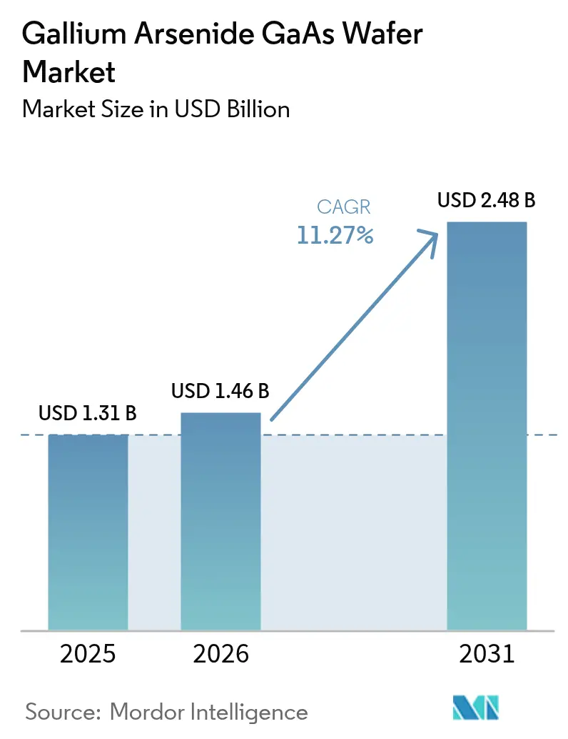
| Market Size (2026) | USD 1.46 Billion |
| Market Size (2031) | USD 2.48 Billion |
| Growth Rate (2026 - 2031) | 11.27% CAGR |
| Fastest Growing Market | Asia Pacific |
| Largest Market | Asia Pacific |
| Market Concentration | Medium |
Major Players *Disclaimer: Major Players sorted in no particular order Image © Mordor Intelligence. Reuse requires attribution under CC BY 4.0. | |
Gallium Arsenide GaAs Wafer Market Analysis by Mordor Intelligence
Gallium arsenide wafer market size in 2026 is estimated at USD 1.46 billion, growing from 2025 value of USD 1.31 billion with 2031 projections showing USD 2.48 billion, growing at 11.27% CAGR over 2026-2031. Robust demand for high-frequency radio modules, optoelectronic emitters, and defense-grade radar devices keeps Gallium arsenide substrates firmly positioned where silicon performance plateaus. Large telecom operators are refreshing network hardware to 5G standards, compelling front-end module suppliers to specify GaAs power amplifiers that outperform CMOS at millimeter-wave bands.[1]Qorvo, “Fiscal 2025 Third Quarter Results,” qorvo.com In parallel, data-center operators adopt VCSEL arrays on GaAs to move 400G and 800G traffic with lower latency, while micro-LED innovators count on GaAs epi uniformity to scale augmented-reality headsets. Investment patterns confirm that Asia-Pacific fabs leverage vertical integration and cost advantages to supply global customers, even as North America rings-fences critical military demand for radiation-hardened wafers. Breakthrough concepts such as remote epitaxy promise to recycle substrates, hinting at future shifts in GaAs consumption economics without dampening near-term demand.
Key Report Takeaways
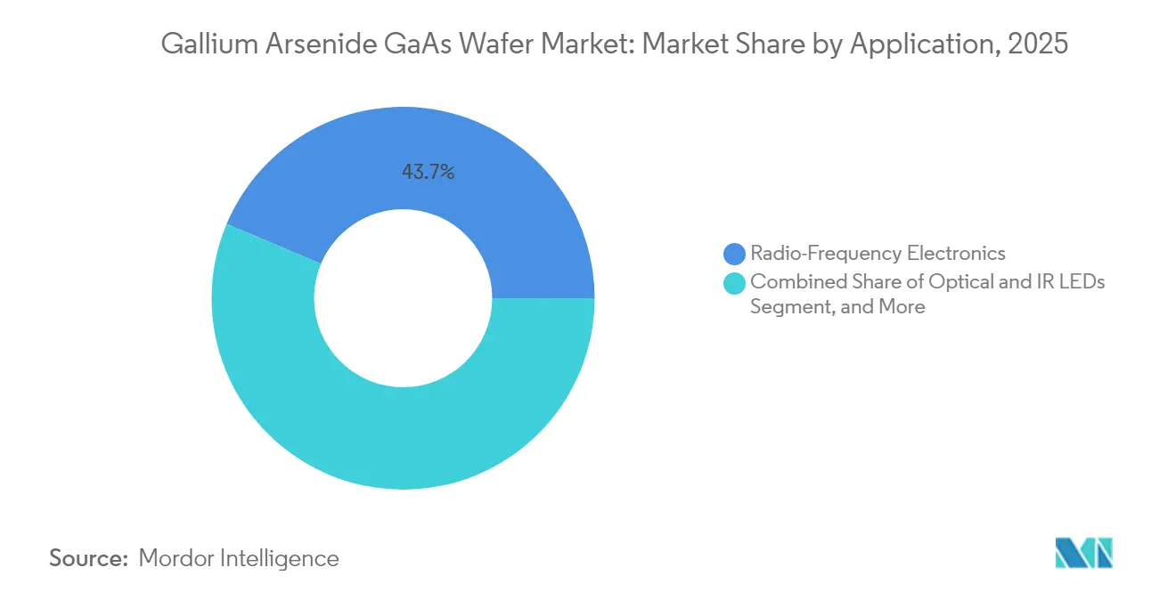
- By application, RF electronics led with 43.65% of the Gallium arsenide wafer market share in 2025; photonic and imaging devices are advancing at a 13.25% CAGR through 2031.
- By wafer diameter, 4-inch substrates accounted for 35.85% of the Gallium arsenide wafer market size in 2025, while 6-inch formats are expanding at a 12.85% CAGR to 2031.
- By growth technology, VGF captured 38.75% of the Gallium arsenide wafer market share in 2025; MBE is set to grow at a 13.1% CAGR over the forecast horizon.
- By end-use industry, telecom and 5G infrastructure commanded 42.35% of the Gallium arsenide wafer market share in 2025, whereas automotive applications recorded the highest projected CAGR at 12.05% through 2031.
- By conductivity type, semi-insulating GaAs retained 53.15% share of the Gallium arsenide wafer market size in 2025, and semi-conducting substrates are forecast to accelerate at 11.95% CAGR to 2031.
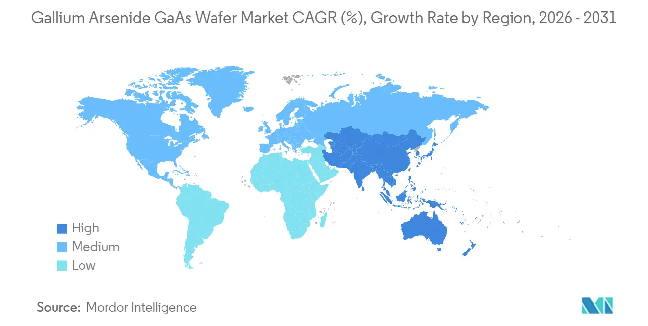
- By geography, Asia-Pacific dominated with 60.10% of the Gallium arsenide wafer market share in 2025 and remains the fastest-growing region at 11.78% CAGR.
Note: Market size and forecast figures in this report are generated using Mordor Intelligence’s proprietary estimation framework, updated with the latest available data and insights as of 2026.
Global Gallium Arsenide GaAs Wafer Market Trends and Insights
Drivers Impact Analysis*
| Driver | (~) % Impact on CAGR Forecast | Geographic Relevance | Impact Timeline |
|---|---|---|---|
| 5G infrastructure roll-out fuels GaAs RF demand | +2.8% | Global with APAC core | Medium term (2-4 years) |
| Optoelectronic device boom (VCSELs, lasers) | +2.1% | Global, Asia-Pacific hubs | Medium term (2-4 years) |
| Aerospace and defense uptake for high-freq radar | +1.6% | North America and Europe | Long term (≥ 4 years) |
| Asian epitaxy capacity boosts supply and lowers ASP | +1.4% | Asia-Pacific | Short term (≤ 2 years) |
| Micro-LED adoption in AR/VR wearables | +1.8% | Global early adoption | Long term (≥ 4 years) |
| Remote-epitaxy substrate reuse cuts wafer cost | +1.7% | Advanced manufacturing regions | Long term (≥ 4 years) |
| Source: Mordor Intelligence | |||
5G Infrastructure Roll-out Fuels GaAs RF Demand
Telecom operators are deploying dense 5G macro- and small-cell sites that require power amplifiers sustaining linear output well above 28 GHz, where silicon LDMOS falters. Gallium arsenide wafers deliver electron mobility around 8,500 cm²/V·s, enabling efficient front-end modules that preserve signal integrity in massive-MIMO arrays for urban coverage. Network vendors lock multiyear supply contracts with vertically integrated GaAs houses, converting 4G hardware refresh cycles into predictable demand through 2027.
Optoelectronic Device Boom (VCSELs, Lasers)
Hyperscale data centers move to 400G and 800G optics that rely on GaAs-based VCSEL arrays for lower latency and power draw. Smartphone makers embed 3D-sensing VCSELs in biometric modules, while automotive OEMs adopt GaAs lasers for LiDAR. Epitaxial regrowth advances improve thermal dissipation, extending device lifetimes and sustaining premium wafer ASPs.
Aerospace and Defense Uptake for High-Frequency Radar
Active electronically scanned arrays in fighter jets and naval radar require thousands of radiation-hard GaAs MMICs that maintain gain over extreme temperatures. Long government procurement cycles secure high-purity semi-insulating substrates, anchoring a steady revenue stream for specialized U.S. and European foundries.[2]IEEE, “GaAs MMIC Reliability and Space Qualification Guide,” ieee.org
Asian Epitaxy Capacity Boosts Supply and Lowers ASP
Taiwanese, South Korean, and mainland Chinese fabs added multi-reactor lines that drive wafer throughput and shorten lead times. Cost advantages from clustering epi, polishing, and metrology under one roof translate into lower average selling prices, widening accessibility for consumer applications.
Restraints Impact Analysis*
| Restraint | (~) % Impact on CAGR Forecast | Geographic Relevance | Impact Timeline |
|---|---|---|---|
| High production cost vs Si and SiC | -1.9% | Global | Short term (≤ 2 years) |
| Gallium supply concentration and export controls | -2.3% | Global, non-Chinese fabs | Medium term (2-4 years) |
| GaN and SiC competition in RF / power | -1.4% | Global | Medium term (2-4 years) |
| Environmental and safety compliance | -0.8% | Developed markets | Long term (≥ 4 years) |
| Source: Mordor Intelligence | |||
High Production Cost vs Si and SiC
GaAs crystal pulling needs pressurized arsenic atmospheres and toxic-gas handling that raise CapEx and Opex above silicon. Smaller 4-inch and 6-inch formats cannot match the die-per-wafer economics of 300 mm silicon, limiting GaAs uptake in price-sensitive consumer gadgets.[3]Stanford Advanced Materials, “Essential Electronic Materials: Part 4 – Gallium Compounds,” samaterials.com
Gallium Supply Concentration and Export Controls
China refines most of the world’s gallium, and new export licensing rules increase material lead times for foreign fabs. Alternative sources exist but require fresh hydrometallurgical capacity, elongating risk-mitigation timelines and pressuring inventories.[4]U.S. Department of Energy, “Low-Cost, High-Efficiency III-V Photovoltaics Enabled by Remote Epitaxy,” energy.gov
*Our forecasts treat driver/restraint impacts as directional, not additive. The impact forecasts reflect baseline growth, mix effects, and variable interactions.
Segment Analysis
By Application: RF Electronics Anchors Demand While Photonics Accelerates
RF electronics held 43.65% revenue in 2025 as power amplifiers and switches remain core to 5G infrastructure upgrades. This portion of the Gallium arsenide wafer market size is forecast to climb steadily alongside small-cell densification plans. Photonic and imaging devices, propelled by VCSEL interconnects and AR/VR optics, are set to outpace all other uses at 13.25% CAGR, thereby reshaping future volumes of the Gallium arsenide wafer market.
Cross-segment pull-through emerges as handset makers integrate VCSEL-based face ID modules, boosting both photonics and RF volume on common 6-inch epi lines. Solar cells on GaAs remain a niche for spacecraft, yet new heterointegration concepts could push multi-junction designs into terrestrial concentrator arrays.


By Wafer Diameter: Transition Toward 6-Inch Formats Gains Momentum
Four-inch substrates still command 35.85% revenue thanks to mature tooling, but capacity announcements reveal that 6-inch lines will absorb most incremental demand at 12.85% CAGR. The shift improves die counts per run and spreads fixed costs, nudging the overall Gallium arsenide wafer market toward lower ASPs.
Equipment vendors tackle thermal-gradient control and arsenic vapor management to scale beyond 6 inches. Early 8-inch pilot runs show promise yet require further defect reduction before commercial deployment.
By Growth Technology: VGF Dominance Meets MBE Precision
VGF yielded 38.75% of revenue in 2025 by balancing throughput with low dislocation density. However, MBE shipments are rising 13.1% annually as quantum dot emitters and telecom lasers need atomic-scale layer control. Hybrid flows combining VGF bulk growth with MBE epi caps are emerging to optimize both cost and performance.
MOCVD enjoys a share in LED and micro-LED backplanes by offering faster growth rates, while LEC remains indispensable for semi-insulating material used in defense radar.
By End-Use Industry: Telecom Leads, Automotive Surges
Telecom infrastructure consumed 42.35% of wafer output in 2025, reflecting relentless 5G roll-outs. Automotive volumes are poised to lift at a 12.05% CAGR as radar and LiDAR modules migrate from silicon to compound semiconductors for longer range and higher resolution.
Consumer electronics sustains steady mid-single-digit growth on handset RF upgrades, whereas aerospace and defense secure a premium niche that values substrate purity over price.

By Conductivity Type: Semi-Insulating Holds Majority, Doped Wafers Gain Ground
Semi-insulating material preserved a 53.15% share in 2025, indispensable for high-isolation RF devices. Doped n-type and p-type wafers are growing 11.95% annually, driven by photonic emitters where controlled carrier densities dictate emission efficiency.
Advanced fabrication now patterns selective regions of contrasting conductivity on one wafer, allowing co-integration of RF and photonic functions and opening fresh design latitude.
Geography Analysis
Asia-Pacific held 60.10% of the Gallium arsenide wafer market in 2025 thanks to clustered epitaxial lines, a deep subcontract base, and state-backed 5G build-outs. Government incentives help mainland China expand compound-semiconductor fabs, while Taiwan and South Korea provide foundry and equipment synergies that reinforce supply diversity.
North America ranks second, anchored by aerospace and defense demand requiring secure on-shore production. Recent CHIPS Act incentives finance new crystal-growth reactors and cleanrooms dedicated to semi-insulating material for radar and satellite programs, cementing long-term domestic supply.
Europe retains strength in automotive and industrial automation. Tier-1 suppliers source GaAs power devices to support ADAS radar and factory sensing, while stringent environmental directives spur circular-economy research on wafer reclamation. Coordinated EU funding backs pilot lines for 150 mm compound-semiconductor substrates, seeking to narrow the capacity gap with Asia.

Competitive Landscape
The Gallium arsenide wafer market features moderate concentration, with vertically integrated players spanning crystal growth, epi, and device fabrication to secure quality and margins. Leading suppliers deploy proprietary VGF and MBE recipes that cut dislocation counts, enabling foundry customers to lift RF yields above 90% per run. Long-term supply agreements with telecom and defense primes create entry barriers for newcomers.
Strategic moves include large-diameter capacity additions in Asia-Pacific, evident in a USD 345 million expansion that will push annual output beyond 1.5 million 6-inch wafers. Simultaneously, U.S. incumbents acquire metrology startups to characterize sub-ppm arsenic vacancies, sharpening device performance for space payloads.
Emerging disruptors focus on remote-epitaxy IP, offering wafer-reuse cycles that could slash substrate cost of ownership by 60%. While not yet commercial, such technology has garnered joint-development agreements with photonics integrators seeking thinner, transferable GaAs membranes.
Gallium Arsenide GaAs Wafer Industry Leaders
AXT Inc.
Freiberger Compound Materials GmbH
Sumitomo Electric Industries, Ltd.
Xiamen Powerway Advanced Material Co., Ltd.
Applied Materials, Inc.
- *Disclaimer: Major Players sorted in no particular order


Recent Industry Developments
- January 2025: MACOM committed USD 345 million to expand compound-semiconductor capacity in Asia-Pacific, targeting 5G and defense sectors.
- January 2025: III-V Epi reported GaAs regrowth advances that cut optical losses in high-power laser diodes.
- December 2024: Coherent sold its U.K. GaAs fab to the Ministry of Defence for USD 25.2 million, safeguarding domestic supply for military programs.
- October 2024: MIT researchers achieved 100% wafer exfoliation using graphene-mediated remote epitaxy, demonstrating multiple GaAs wafer reuse cycles.


Global Gallium Arsenide GaAs Wafer Market Report Scope
GaAs wafers find application in ultra-high radio frequency and fast electronic switching applications. GaAs Wafer is an III-V direct bandgap compound semiconductor used for multiple applications. It is a mixture of two elements: Gallium (Ga) and Arsenide (As) and has a zinc blend crystal structure. GaAs has a direct bandgap that allows the emission and absorption of light efficiently. It has exceptionally high electron mobility, which enables GaAs transistors to perform at frequencies exceeding 250 GHz and reduces the noise at which high frequencies tend to lessen the electrical signal disturbance in electronic circuits. GaAs wafers have a broad temperature functioning range or high thermal strength.
The Gallium Arsenide GaAs Wafer Market provides a detailed insight into the current market trends, demand across major end-user industries, and emerging future opportunities. The study segments the market by Application (Radio Frequency Electronics, Light Emitting Diodes, Photovoltaic Devices, Phototonic Devices) and Geography (United States, Taiwan, China, Japan, United Kingdom, Germany, and Rest of the World). The report offers the market size in value terms in USD for all the abovementioned segments.
| Radio-Frequency Electronics |
| Optical and IR LEDs |
| Photovoltaic / Solar Cells |
| Photonic and Imaging Devices |
| Other Applications |
| 2 inch (50 mm) |
| 3 inch (76 mm) |
| 4 inch (100 mm) |
| 6 inch (150 mm) |
| 8 inch (200 mm) and Above |
| Liquid-Encapsulated Czochralski (LEC) |
| Vertical Gradient Freeze (VGF) |
| Horizontal Bridgman (HB) |
| Molecular Beam Epitaxy (MBE) |
| Metal-Organic CVD (MOCVD) |
| Telecom and 5G Infrastructure |
| Consumer Electronics |
| Aerospace and Defense |
| Automotive (ADAS, EV) |
| Industrial and Energy |
| Semi-insulating GaAs |
| Semi-conducting GaAs (n-/p-type) |
| North America | United States |
| Canada | |
| Mexico | |
| South America | Brazil |
| Argentina | |
| Rest of South America | |
| Europe | Germany |
| United Kingdom | |
| France | |
| Italy | |
| Rest of Europe | |
| Asia-Pacific | China |
| Japan | |
| South Korea | |
| India | |
| Rest of Asia-Pacific | |
| Middle East | Saudi Arabia |
| United Arab Emirates | |
| Rest of Middle East | |
| Africa | South Africa |
| Rest of Africa |
| By Application | Radio-Frequency Electronics | |
| Optical and IR LEDs | ||
| Photovoltaic / Solar Cells | ||
| Photonic and Imaging Devices | ||
| Other Applications | ||
| By Wafer Diameter | 2 inch (50 mm) | |
| 3 inch (76 mm) | ||
| 4 inch (100 mm) | ||
| 6 inch (150 mm) | ||
| 8 inch (200 mm) and Above | ||
| By Growth Technology | Liquid-Encapsulated Czochralski (LEC) | |
| Vertical Gradient Freeze (VGF) | ||
| Horizontal Bridgman (HB) | ||
| Molecular Beam Epitaxy (MBE) | ||
| Metal-Organic CVD (MOCVD) | ||
| By End-Use Industry | Telecom and 5G Infrastructure | |
| Consumer Electronics | ||
| Aerospace and Defense | ||
| Automotive (ADAS, EV) | ||
| Industrial and Energy | ||
| By Conductivity Type | Semi-insulating GaAs | |
| Semi-conducting GaAs (n-/p-type) | ||
| By Geography | North America | United States |
| Canada | ||
| Mexico | ||
| South America | Brazil | |
| Argentina | ||
| Rest of South America | ||
| Europe | Germany | |
| United Kingdom | ||
| France | ||
| Italy | ||
| Rest of Europe | ||
| Asia-Pacific | China | |
| Japan | ||
| South Korea | ||
| India | ||
| Rest of Asia-Pacific | ||
| Middle East | Saudi Arabia | |
| United Arab Emirates | ||
| Rest of Middle East | ||
| Africa | South Africa | |
| Rest of Africa | ||


Key Questions Answered in the Report
How large is the Gallium arsenide wafer market in 2026?
It is valued at USD 1.46 billion, with an 11.27% CAGR projected through 2031.
Which application currently generates the most wafer demand?
RF electronics for 5G infrastructure accounts for 43.65% of 2025 revenue.
Why are 6-inch substrates gaining popularity?
They offer better die economics, driving 12.85% CAGR while equipment advances manage thermal stresses.
What region dominates GaAs wafer manufacturing?
Asia-Pacific holds 60.10% share due to dense epitaxial capacity and robust 5G investments.
How do export controls impact supply?
China¢s tight gallium control can lengthen lead times for non-Chinese fabs, adding a -2.3% drag on forecast CAGR.
Are alternative crystal growth methods emerging?
Yes, remote epitaxy enables wafer reuse and MBE adoption is rising 13.1% annually for precision heterostructures.
Page last updated on:


