
GaN Semiconductor Devices Market Size and Share
Market Overview
| Study Period | 2020 - 2031 |
|---|---|
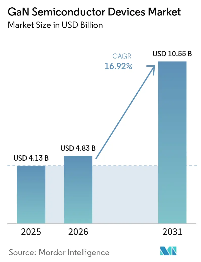
| Market Size (2026) | USD 4.83 Billion |
| Market Size (2031) | USD 10.55 Billion |
| Growth Rate (2026 - 2031) | 16.92 % |
| Fastest Growing Market | Asia Pacific |
| Largest Market | Asia Pacific |
| Market Concentration | Medium |
Major Players
*Disclaimer: Major Players sorted in no particular order Image © Mordor Intelligence. Reuse requires attribution under CC BY 4.0. |
|
GaN Semiconductor Devices Market Analysis by Mordor Intelligence
The gallium nitride semiconductor devices market size in 2026 is estimated at USD 4.83 billion, growing from 2025 value of USD 4.13 billion with 2031 projections showing USD 10.55 billion, growing at 16.92% CAGR over 2026-2031. The surge mirrors GaN’s intrinsic ability to deliver higher efficiency, faster switching, and superior thermal performance when compared with legacy silicon. Market momentum was reinforced in 2024 and early 2025 by three concurrent shifts: 800 V electric-vehicle powertrains, large-scale 5G rollouts that require high-power radio-frequency amplifiers, and consumer demand for ultra-compact USB-C chargers exceeding 100 W. At the same time, global energy-efficiency regulations tightened, pushing data-center operators and industrial OEMs toward GaN-based conversion stages that cut losses and shrink cooling overhead. Corporate investment underscored the trend as Infineon, Renesas, and other incumbents expanded GaN capacity through acquisitions, while regional incentives in Japan and the European Union accelerated green-field fabs geared to 6-inch and 8-inch wafers.
Key Report Takeaways
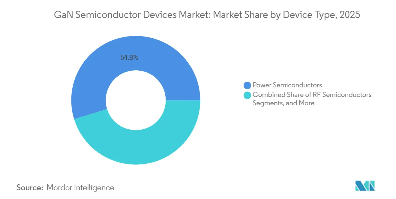
- By device type, power semiconductors led with 54.78% of the gallium nitride semiconductor devices market share in 2025; RF devices are projected to advance at a 18.73% CAGR through 2031.
- By component, discrete transistors accounted for 56.63% share of the gallium nitride semiconductor devices market size in 2025, while monolithic power ICs are set to expand at a 29.55% CAGR.
- By voltage rating, the 100-650 V class captured 69.72% revenue share in 2025; the >650 V segment grows fastest at 39.67% CAGR on the back of 800 V EV platforms.
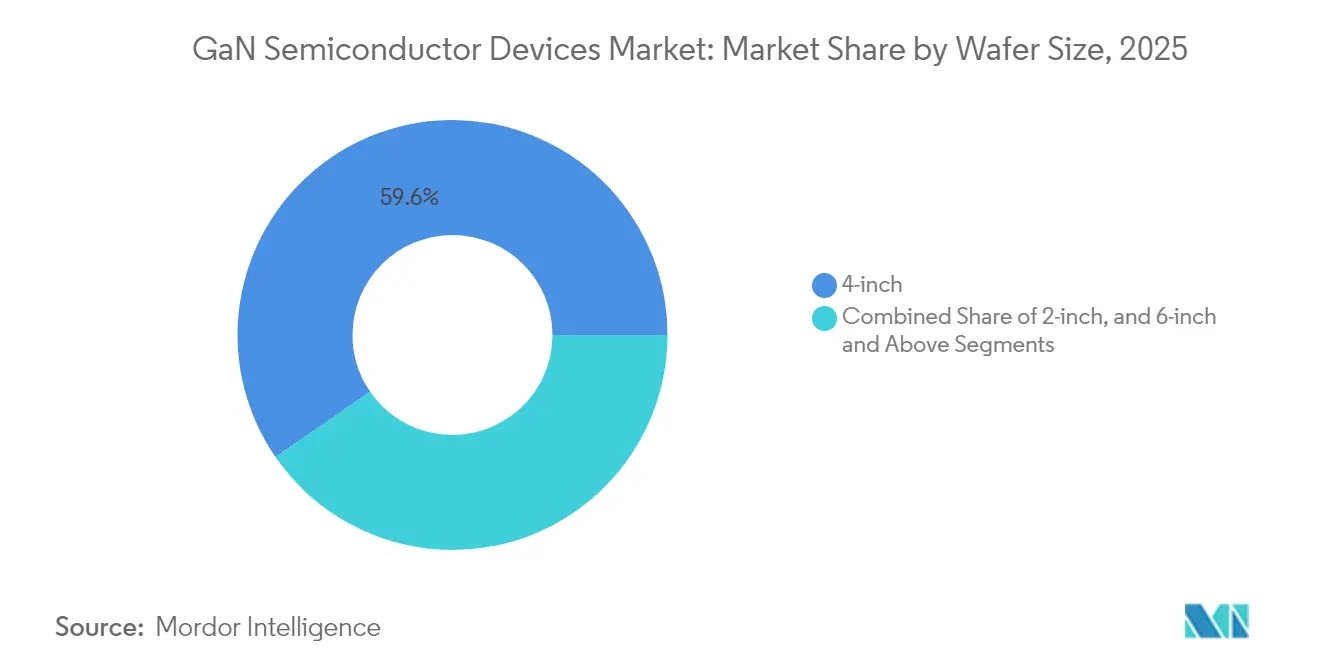
- By wafer size, 4-inch substrates dominated with a 59.61% share in 2025; 6-inch and 8-inch production lines are forecast to grow at a 35.62% CAGR as cost parity approaches.
- By substrate technology, GaN-on-SiC maintained a 59.74% share in 2025; GaN-on-Si is the fastest rising at 40.09% CAGR through 2031.
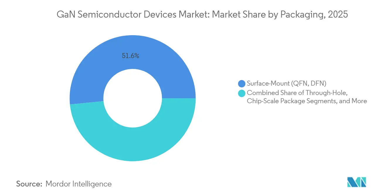
- By packaging, surface-mount formats such as QFN held 51.58% share in 2025; chip-scale packages deliver the highest pace at 34.66% CAGR.
- By end-user industry, telecom and datacom infrastructure represented 34.72% of 2025 revenue while automotive and e-mobility matched that segment’s 33.70% CAGR to 2031.
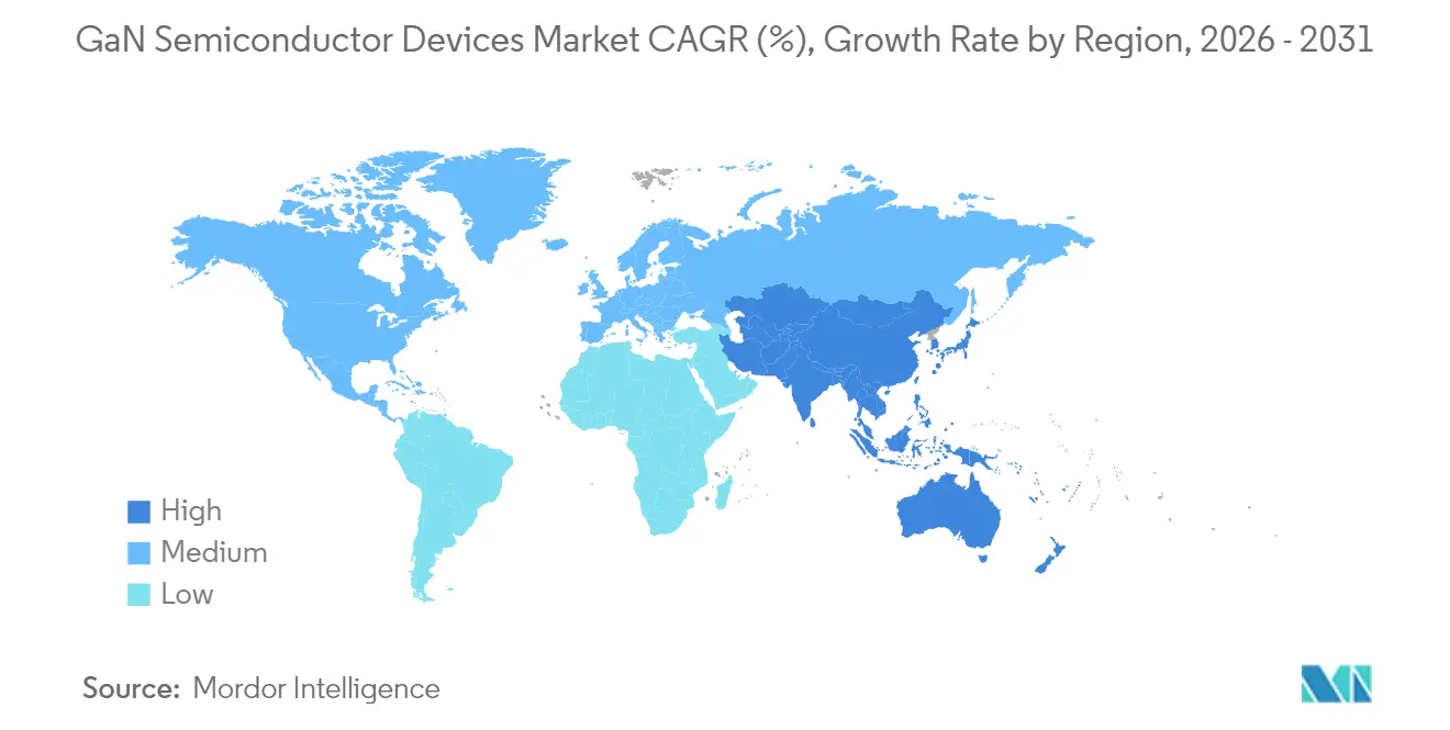
- By geography, Asia-Pacific commanded a 37.85% share in 2025; it also posts the quickest regional expansion at a 28.35% CAGR to the end of the decade.
Note: Market size and forecast figures in this report are generated using Mordor Intelligence’s proprietary estimation framework, updated with the latest available data and insights as of 2026.
Market Trends and Insights
Drivers Impact Analysis of GaN Semiconductor Devices Market*
| Driver | (~) % Impact on CAGR Forecast | Geographic Relevance | Impact Timeline |
|---|---|---|---|
| Proliferation of 65-240 W USB-C PD GaN Chargers Led by Chinese OEM Road-maps | +3.2% | Global, with the highest impact in Asia-Pacific and North America | Short term (≤ 2 years) |
| 5G Massive-MIMO Macro-Cell Roll-outs Requiring >200 W GaN-on-SiC PAs in Asia and India | +4.1% | Asia-Pacific with a focus on China, India, Japan, and South Korea | Medium term (2–4 years) |
| Shift to 800 V EV Platforms Driving Bidirectional GaN OBC and DC-DC Adoption | +3.8% | Global with early uptake in Europe, China, and North America | Medium term (2–4 years) |
| Weight-Critical More-Electric Aircraft and eVTOL Powertrains Selecting GaN Converters | +1.9% | North America and Europe | Long term (≥ 4 years) |
| LEO Constellation Satellites Migrating to GaN Ku/Ka-Band SSPAs | +1.5% | Global, with development centered in North America and Europe | Medium term (2–4 years) |
| Japanese and EU Fab Incentives Accelerating GaN Capacity Expansion | +2.7% | Japan and Europe | Medium term (2–4 years) |
| Source: Mordor Intelligence | |||


Proliferation of 65-240 W USB-C PD GaN Chargers Led by Chinese OEM Road-maps
Chinese consumer-electronics brands propelled a rapid shift toward ultra-compact universal serial bus power-delivery chargers. Models released in 2024 delivered up to 240 W while shrinking volume by 40% relative to silicon equivalents and lowering retail prices by 35%. Anker’s GaN Prime line exceeded 1.8 W/cm³ power density, enabling multiprotocol charging for laptops and phones within pocket-sized enclosures.[1]Anker Innovations, “Anker GaN Prime Series Specifications,” anker.com Cost-downs stimulated mainstream uptake across Asia-Pacific and North America, lifting unit volumes that ripple across the gallium nitride semiconductor devices market.
5G Massive-MIMO Macro-Cell Roll-outs Requiring >200 W GaN-on-SiC PAs in Asia and India
Mobile network operators in China, India, and Japan deployed more than 15,000 macro base stations in 2024 using GaN-on-SiC power amplifiers above 3.5 GHz. The switch trimmed power consumption by 25% and stretched coverage by 18%, translating into USD 18 million annual operating expense savings for one leading Japanese carrier. Such economics cement GaN PA design wins and expand addressable revenue across the gallium nitride semiconductor devices market.
Shift to 800 V EV Platforms Driving Bidirectional GaN OBC and DC-DC Adoption
Luxury electric-vehicle platforms launched in Europe and China during 2024 integrated bidirectional GaN onboard chargers operating at 800 V. The architecture slashed 10-80% state-of-charge times to under 20 minutes and allowed vehicle-to-grid services that can earn owners up to USD 1,200 each year. Efficiency hit 97.5%, outperforming comparable SiC stages by 2.8% and reducing cooling mass by 40% which fuels growth across the gallium nitride semiconductor devices market.
Weight-Critical More-Electric Aircraft and eVTOL Powertrains Selecting GaN Converters
A leading aircraft OEM replaced silicon modules with GaN converters in primary distribution units, shedding 125 kg system weight and raising conversion efficiency by 3.8%. Lifetime fuel savings were valued at USD 1.4 million per aircraft. Such data reinforced confidence in GaN for aviation, opening a long-term runway for the gallium nitride semiconductor devices market. Cumulatively, data-center adoption supports the higher-margin portion of the GaN-on-silicon technology market and reinforces confidence in long-term capacity expansion.
Restraints Impact Analysis of GaN Semiconductor Devices Market*
| Restraint | (~) % Impact on CAGR Forecast | Geographic Relevance | Impact Timeline |
|---|---|---|---|
| Limited 200 mm GaN-on-Si Epi Wafer Supply Chain Bottlenecks | –2.1% | Global with the highest impact in Asia-Pacific | Medium term (2–4 years) |
| Gate Reliability Challenges >175 °C for Automotive Grade-0 Qualification | –1.8% | Global, particularly affecting automotive applications | Medium term (2–4 years) |
| Cost Delta vs. LDMOS in Sub-3.5 GHz Macro PAs in Emerging Markets | –1.3% | Emerging markets in Asia, Africa, and Latin America | Short term (≤ 2 years) |
| Fragmented Test/Packaging Ecosystem for E-mode GaN QFN/CSP Packages | –1.6% | Global | Short term (≤ 2 years) |
| Source: Mordor Intelligence | |||
Limited 200 mm GaN-on-Si Epi Wafer Supply Chain Bottlenecks
Fewer than 10 qualified suppliers produced 200 mm GaN epitaxial wafers in 2024. Yields sat 15-20% below silicon benchmarks, constraining throughput and sustaining premium pricing. A European Tier-1 automotive supplier recorded a six-month production delay that forced strategic inventory buffers worth EUR 28 million (USD 30.2 million). Bottlenecks weigh on near-term volumes within the gallium nitride semiconductor devices market.
Gate Reliability Challenges >175 °C for Automotive Grade-0 Qualification
Charge-trapping at the gate interface still causes threshold drift at 175 °C. A Japanese components maker postponed product launch by 11 months in 2024 after high-temperature stress tests failed, adding JPY 420 million (USD 2.8 million) in redesign costs. These reliability hurdles slow adoption in under-hood environments and temper growth across the gallium nitride semiconductor devices market.
*Our forecasts treat driver/restraint impacts as directional, not additive. The impact forecasts reflect baseline growth, mix effects, and variable interactions.
GaN Semiconductor Devices Market Segment Analysis
By Device Type:
Power Semiconductors Dominate Efficiency RevolutionThe power-semiconductor slice of the gallium nitride semiconductor devices market held 54.78% share in 2025 and is projected to compound at 18.41% to 2031. Data-center operators saved USD 2.3 million per facility by upgrading to GaN server power supplies that reached 98.2% efficiency. RF devices followed as 5G massive-MIMO infrastructure and defense radar sustained premium demand. Maturity signaled a strategic fork. Silicon incumbents such as Infineon expanded automotive-grade GaN MOSFET lines, while RF specialists like Wolfspeed leveraged GaN-on-SiC thermal headroom for >3.5 GHz macro cells. Integrated power-stage providers captured a higher margin by moving beyond discrete sales. The gallium nitride semiconductor devices market, therefore, experiences both consolidation and vertical integration, reinforcing scale advantages.


By Component:
Transistors Lead While Power ICs SurgeHigh-electron-mobility transistors occupied 56.63% revenue in 2025, yet monolithic power ICs outpaced all other categories at 29.55% CAGR. A Chinese smartphone OEM cut the charger bill-of-materials by 18% by replacing discrete switches with a single GaN IC, shrinking part count by 45% and catalyzing volume ramps. Integration improves electromagnetic compatibility and trims parasitics, benefits that explain why the gallium nitride semiconductor devices market is tilting toward system-in-package designs. Module suppliers address high-power installations, while diode sales remain steady in auxiliary rectification roles.
By Voltage Rating:
Higher Voltages Drive GrowthThe 100-650 V corridor kept a 69.72% share in 2025 as it aligns with consumer, data-center, and 48 V industrial rails. Meanwhile, the >650 V band races ahead at 39.67% CAGR, fueled by 800 V propulsion architectures. One premium EV brand slashed 10-80% charge time to 28 minutes using 900 V GaN stages and cut charger mass by 3.2 kg versus SiC. This transition prompts new isolation and test standards, challenging pure-play suppliers. Nevertheless, the gallium nitride semiconductor devices market rewards those able to validate reliability beyond 650 V, unlocking lucrative automotive value pools.
By Wafer Size:
Scaling Drives Cost ReductionFour-inch wafers represented 59.61% shipments in 2025, but 6-inch and 8-inch lines grew 35.62% CAGR as volume demand jumped. A Japanese foundry’s shift to 6-inch boosted die output 140% and reduced unit cost 32%, achieving capital payback in under 20 months. Toyota Gosei’s lab-grown 8-inch bulk GaN crystal and Innoscience’s dedicated 8-inch GaN-on-Si fab exemplify the scale wave. As yields climb, the gallium nitride semiconductor devices market has an avenue to price parity with silicon in mainstream appliances.
By Substrate Technology:
GaN-on-Si Challenges SiC DominanceGaN-on-SiC still held a 59.74% share in 2025 due to telecom and defense thermal requirements. GaN-on-silicon is gaining attention in the GaN substrate market because of its compatibility with large-diameter wafer manufacturing and potential cost advantages. Yet GaN-on-Si topped growth charts at 40.09% CAGR as 8-inch CMOS lines reached cost parity. A satellite operator paid a 45% performance premium for GaN-on-SiC PAs and extended payload life, while a laptop-charger brand shaved costs by 28% using GaN-on-Si with negligible thermal penalties. Thus, the gallium nitride semiconductor devices market bifurcates cost-sensitive mass electronics gravitating to Si platforms, whereas mission-critical RF and aerospace remain SiC strongholds.
By Packaging:
Miniaturization Accelerates CSP AdoptionSurface-mount QFN and DFN packages held a 51.58% share in 2025 and remain at baseline. Chip-scale packages have advanced 34.66% CAGR since they permit sub-2 mm z-height and superior thermal resistance. A 67 W smartphone adaptor employing CSP GaN reduced total volume by 48%, enhancing differentiation in premium handset ecosystems. Packaging innovation drives power density, reliability, and EMC compliance, which in turn expands addressable sockets across the gallium nitride semiconductor devices market.
By End-User Industry:
Telecom and Automotive Lead AdoptionTelecom/datacom infrastructure generated 34.72% revenue in 2025. Operators that switched to GaN PAs lowered network energy by 28% and freed USD 24 million operational savings each year, freeing budget for additional cell densification. Automotive mirrored this momentum with a 33.70% CAGR as OEMs chased faster charging, bi-directional flow, and lightweight inverters. Consumer electronics retain healthy demand for 100 W-plus USB-C bricks, while industrial automation and renewable-energy systems accelerate as regulatory efficiency targets converge. All verticals collectively reinforce scale dynamics inside the gallium nitride semiconductor devices market.
Geography Analysis
APAC, North America, EMEA and LATAM GaN Semiconductor Devices Market
Asia-Pacific commanded 37.85% of 2025 sales and remained the fastest riser at 28.35% CAGR. China’s access to gallium, plus state subsidies, allowed Innoscience to operate the world’s largest 8-inch GaN-on-Si plant at costs 35% below peers. South Korea’s consumer-electronics titans and Japan’s automotive majors seeded high-volume anchor customers, sustaining a virtuous cycle of demand and capacity growth. North America stayed an innovation hotbed. Federal CHIPS grants of USD 35 million helped GlobalFoundries broaden GaN capacity in Vermont. Defense contractors deployed GaN-based phased-array radars that boosted detection range by 42% while trimming power by 18%, showcasing mission-critical gains that flow into the gallium nitride semiconductor devices market. Europe prioritized premium automotive and industrial use cases. Cambridge GaN Devices raised EUR 30.5 million (USD 33.1 million) for expansion, reflecting investor belief in high-power European niches. A leading German OEM realized 97.8% charger efficiency and 30% component reduction, aligning with EU eco-design directives. Latin America, the Middle East, and Africa presently hold modest shares yet demonstrate promising uptake in telecom and smart-city projects as energy prices and infrastructure buildouts converge.

Regulatory Landscape
Trade and export-control policy has become a more direct determinant of GaN device commercialization alongside traditional RoHS/REACH compliance. In January 2026, a US proclamation adjusted imports of semiconductors and related products into the United States under Section 232, adding a tariff layer that influences sourcing decisions for GaN devices and the equipment and materials used to make them.
Controls have also tightened around specific GaN form factors and performance claims. In May 2026, the US Department of Commerce, Bureau of Industry and Security expanded export controls to include thermally enhanced QFN-packaged GaN power modules (ECCN 3A001.b.3.2), which raises licensing and screening overhead for certain destinations. In Japan, METI initiated a 90-day special import review in July 2026 for GaN power modules focused on thermal resistance documentation aligned to JEDEC JESD51-14, reinforcing that market access can hinge on standardized, auditable thermal-measurement data for high-density power packaging.
Value Chain Analysis
The GaN semiconductor devices value chain spans upstream raw materials and substrates (gallium feedstock and GaN-on-Si/GaN-on-SiC/bulk GaN substrates), epitaxy (MOCVD GaN epiwafer growth), device fabrication at IDMs and merchant foundries, and assembly, packaging, and test (QFN/DFN, CSP, and power modules), before distribution through OEM and module/inverter/power-supply channels into end markets such as chargers, telecom RF power amplifiers, and automotive power conversion. A structural risk sits upstream, since refined gallium supply is heavily tied to China, and the broader compound semiconductor supply chain has faced added friction following late-2024 US Entity List actions and subsequent Chinese export-control updates affecting gallium and related materials.
On the manufacturing side, capacity is split between vertically integrated IDMs (for example, Infineon and Renesas/Transphorm) and fabless device designers (for example, EPC and Navitas) that rely on merchant foundry ecosystems. The current landscape highlights merchant and partner capacity anchors including GlobalFoundries (Burlington, Vermont, United States) and Powerchip Semiconductor Manufacturing Corporation in Taiwan for 200 mm GaN-on-silicon ramps. The foundry map is also shifting: TSMC confirmed a phase-out of its GaN wafer foundry business (July 2025), pushing qualification work and supply continuity toward specialized foundries and more integrated supply strategies, including ROHM integrating TSMC process technology into its Hamamatsu operations to build an end-to-end production system within the ROHM Group.
Competitive Landscape
Consolidation intensified through 2024-2025. Infineon paid USD 830 million for GaN Systems, and Renesas absorbed Transphorm for USD 339 million, integrating device IP and customer channels. Power Integrations followed suit by acquiring Odyssey Semiconductor. These moves signalled an inflection where the gallium nitride semiconductor devices industry moved from niche to mainstream.
Competitive strategy is split along technology lines. Navitas championed fully integrated GaNFast ICs, lowering design complexity for charging and solar micro-inverter partners.[4]Navitas Semiconductor, “GaNFast Integrated Power IC Road-map,” navitassemi.com EPC supplied bare-die and eGaN FETs for custom layouts in lidar and satellites. Substrate specialization also defined turf: Wolfspeed defended GaN-on-SiC for X-band radar, while Innoscience pushed cost-optimized GaN-on-Si into mobile accessories. Patent activity underpinned rivalry with more than 2,400 GaN-related filings logged in 2024.
Barriers to entry rose as qualification cycles, automotive grade requirements, and supply agreements locked in incumbents. Nonetheless, fab-less start-ups that master design-for-integration can still find niches, especially in AI datacenter power, where vertical-specific reference platforms create a ready beachhead inside the gallium nitride semiconductor devices market.
GaN Semiconductor Devices Industry Leaders
-
Infineon Technologies AG
-
Wolfspeed Inc.
-
Qorvo Inc.
-
Navitas Semiconductor
-
Transphorm Inc.
- *Disclaimer: Major Players sorted in no particular order

GaN Semiconductor Devices Market Companies Covered in this Report
- Efficient Power Conversion Corporation
- Navitas Semiconductor
- Transphorm Inc.
- Innoscience Technology Co., Ltd.
- MACOM Technology Solutions Holdings, Inc.
- Tagore Technology Inc.
- VisIC Technologies Ltd.
- Cambridge GaN Devices Ltd.
- NexGen Power Systems, Inc.
- Qromis, Inc.
- EPC Space LLC
- Analog Devices, Inc.
- Power Integrations, Inc.
- Ommic SAS
- Wolfspeed GaN Solutions
- Ampleon Netherlands B.V.
- Integra Technologies, Inc.
- RFHIC Corporation
- Sumitomo Electric Device Innovations Inc.
- Infineon Technologies AG
- STMicroelectronics N.V.
- Qorvo Inc.

Market Opportunities and Future Outlook
Near-term whitespace concentrates around scaling GaN-on-silicon to 200 mm and beyond while meeting tighter reliability and thermal and EMI requirements in automotive and infrastructure power. Concrete actions in 2025-2026 show the industry organizing around larger-wafer manufacturing and localized supply: Navitas Semiconductor partnered with Powerchip (announced July 2025) to move 200 mm GaN-on-silicon production to Powerchip Fab 8B in Taiwan, and GlobalFoundries and Navitas announced a long-term partnership (November 2025) to manufacture next-generation GaN technology at GlobalFoundries Burlington. In parallel, onsemi and GlobalFoundries announced a collaboration in January 2026 to manufacture 650 V GaN power devices at Burlington, tying volume manufacturing closer to named fabs for AI power infrastructure and EV power conversion.
Opportunities also extend upstream and midstream where bottlenecks have been visible, especially in epi and substrate supply, as well as in the packaging and test ecosystem for compact, high-power modules. ROHM (February 2026) disclosed steps to integrate its GaN development and manufacturing with TSMC process technology to form an end-to-end production system, and later partnered with Aixtron (June 2026) to install G10-GaN MOCVD systems at Hamamatsu to bring epitaxy in-house for 650 V and 100 V platforms. On the materials side, Mitsubishi Chemical and Japan Steel Works (July 2026) announced plans to ramp GaN substrate capacity for EV and data center power systems, while GlobalWafers (May 2026) initiated a phased GaN capacity expansion aimed at high-efficiency power solutions in AI servers. These moves align with the report scope where monolithic power ICs, higher-voltage classes, and advanced packaging (including chip-scale packages) are gaining share, since they reduce parts count and help systems meet efficiency and thermal constraints.
Recent Industry Developments in GaN Semiconductor Devices Market
- July 2026: Infineon Technologies reported that the US International Trade Commission confirmed its final determination after the Presidential Review Period, maintaining import and sales bans against Innoscience for patent infringement related to GaN technology. The decision strengthens enforceable IP boundaries in a key end-market geography and can reshape supplier access for GaN devices and modules sold into US channels.
- July 2025: Navitas Semiconductor announced a partnership with Powerchip Semiconductor Manufacturing Corporation to move 200 mm GaN-on-silicon production to Powerchip Fab 8B in Taiwan. The agreement targets scale-up and cost-down priorities for high-volume power GaN and adds foundry options as the ecosystem shifts away from legacy 150 mm capacity.
- May 2024: Mobile network operators in China, India, and Japan deployed more than 15,000 macro base stations using GaN-on-SiC power amplifiers above 3.5 GHz. The rollout reinforced GaN-on-SiC as a performance anchor for high-power RF and supported a demand pull-through for qualified wafers, packaging, and test capacity aligned to telecom infrastructure programs.


GaN Semiconductor Devices Market Report Scope and Research Methodology
Market Definition and Coverage
For this methodology, the GaN semiconductor devices market covers revenue earned from GaN based electronic devices sold as discrete components or integrated devices, which are then used in end equipment such as consumer electronics, automotive, ICT, aerospace and defense, and medical.
Scope exclusions: We do not count full end systems that only contain GaN components (such as complete chargers or inverters), and we also exclude GaN substrates and epitaxial wafers sold as materials rather than devices.
Segments Covered in This Report
-
By Device Type
- Power Semiconductors
- RF Semiconductors
- Opto-Semiconductors
-
By Component
- Transistors (HEMT/FET)
- Diodes (Schottky, PiN)
- Rectifiers
- Power ICs (Monolithic, Multi-chip)
- Modules (Half-bridge, Full-bridge)
-
By Voltage Rating
- < 100 V
- 100 – 650 V
- > 650 V
-
By Wafer Size
- 2-inch
- 4-inch
- 6-inch and Above (incl. 8-inch Pilot)
-
By Substrate Technology
- GaN-on-SiC
- GaN-on-Si
- GaN-on-Sapphire
- Bulk GaN
- 650 – 1200 V
- > 1200 V
-
By Packaging
- Surface-Mount (QFN, DFN)
- Through-Hole (TO-220, TO-247)
- Chip-Scale Package (CSP)
- Bare Die
-
By End-User Industry
-
Automotive and Mobility
- Electric Vehicles
- Charging Infrastructure
-
Consumer Electronics
- Smartphone Fast Chargers
- Laptop and Tablet Chargers
- Gaming Consoles and VR
-
Telecom and Datacom
- 5G Base Stations
- Data Center Power
-
Industrial and Energy
- Solar Inverters
- Motor Drives
- Power Supply Units (SMPS)
-
Aerospace and Defense
- Radar Systems
- Electronic Warfare
- Satellite Payloads
-
Medical
- MRI and CT
- Portable Medical Devices
-
Automotive and Mobility
-
By Geography
-
North America
- United States
- Canada
- Mexico
-
South America
- Brazil
- Argentina
- Rest of South America
-
Europe
- Germany
- United Kingdom
- France
- Italy
- Spain
- Rest of Europe
-
Asia-Pacific
- China
- Japan
- South Korea
- India
- Taiwan
- Rest of Asia-Pacific
-
Middle East and Africa
-
Middle East
- Saudi Arabia
- United Arab Emirates
- Turkey
- Rest of Middle East
-
Africa
- South Africa
- Rest of Africa
-
Middle East
-
North America
Data Sources, Market Sizing, and Validation
Desk Research
Desk research was used to build the market base and keep assumptions tied to signals that can be checked again later. We leaned on public datasets and technical references to understand where GaN is being adopted and why performance requirements are shifting.
Common inputs included sources such as US ITC trade data for electronics flows, US DOE materials and power electronics publications, IEEE and other peer reviewed journals for device performance trends, USPTO patent filings to track new designs, and IEA outlooks for EV and power infrastructure demand. We also reviewed company annual reports, investor presentations, and reputable press for capacity additions and product launches, and we used a paid subscription for company financials and another for patent analytics to reduce gaps in coverage. These examples are not exhaustive, and other public sources were referenced for collection, validation, and clarification.
Primary Interviews and Surveys
Primary inputs were gathered through expert interviews and structured surveys with people close to GaN device design, manufacturing, packaging, and procurement, including device makers, foundries, module partners, and OEM engineering and sourcing teams. Since adoption is global, inputs were validated across APAC, EMEA, and the Americas to capture differences in supply ramps and end demand timing.
The respondent feedback helped confirm which device categories were being treated as "devices" versus "modules" in procurement and product reporting, and it also refined assumptions around packaging changes that affect usable revenue per unit.
Distribution of primary research fieldwork respondents
| Company type | Respondent position | Region |
|---|---|---|
| Top tier: 25% | CXOs: 13% | APAC: 50% |
| Mid tier: 58% | Functional/Unit leaders: 31% | EMEA: 30% |
| Smaller Players: 17% | Managers: 56% | Americas: 20% |
Market-Sizing & Forecasting
Market size was first constructed using a top-down approach that rebuilds the demand pool from end-use adoption, and then converts it into device revenue using GaN specific penetration and pricing assumptions. In practice, we start from demand indicators in automotive, consumer charging, data center power, and telecom infrastructure, and then we apply realistic GaN share and content-per-system factors that were checked with industry participants.
To keep totals practical, a few key inputs were tracked closely, such as shipments of fast chargers and adapters, EV onboard charger and DC-DC adoption, 5G base station and RF power amplifier demand, wafer size migration (2-inch to 6-inch and above), and typical ASP movement as yields improve and packaging changes. Where data was thin for a niche use case, gap filling was handled through range based assumptions that were later narrowed using interview feedback tied to real product roadmaps.
Selective bottom-up approximations were used to corroborate the total, mainly by sampling reported revenues, product mix cues, and volume times ASP checks for representative device families. For forecasting, scenario analysis was used around adoption speed and ASP decline, and then a simple multivariate regression linked demand growth to macro drivers like EV sales and data center buildouts, which were stress tested with expert views.
Data Validation & Update Cycle
Validation was done by triangulating results across multiple checks, so one input could not overly drive the final number. Model outputs were compared with independent signals like end-market shipment trends, capacity expansion announcements, and wafer size transition timing, followed by variance checks across regions and end uses.
Before sign-off, the work goes through a multi-step review where assumptions are re-tested and outliers are challenged, and respondents are re-contacted when new information creates a material mismatch. Reports are refreshed annually, with interim updates when major events change supply, demand, or pricing, and a final pre-delivery scan is completed so clients receive the latest view.
Mordor Intelligence's Gan Semiconductor Devices Market Sizing Compared With Other Published Estimates
Published market sizes for GaN semiconductor devices often do not match, mainly because each publisher draws the line differently around what counts as a device, which applications are included, and what year is used as the starting point. Differences also come from how quickly pricing is assumed to fall as wafer sizes scale and yields improve, and whether conservative or aggressive adoption scenarios are reported.
The table shows a wide spread because some estimates fold in adjacent revenue pools like system level power modules or broader GaN materials, while others keep the scope tighter around discrete and integrated devices. In Mordor Intelligence's model, power, opto-semiconductors, and RF devices are counted as device revenues across end industries, and system level equipment value is kept out, which changes the total even when similar adoption drivers are used.
Benchmark comparison
| Source | Market Size | Gaps in Research Methodology |
|---|---|---|
| Mordor Intelligence | USD 4.83 B (2026) | |
| Global Consultancy A | USD 3.06 B (2024) | Uses an earlier base year and a different normalization of ASPs, and it also reports a faster ramp that can inflate later years if early penetration is assumed higher in consumer and ICT uses. |
| Industry Publisher B | USD 3.70 B (2025) | Uses a different base year and may apply broader device-to-module treatment and longer-horizon assumptions that can change near-term sizing depending on what is counted as a device versus a system component. |
Across the three figures, most of the variance ties back to scope boundaries and base-year choices, followed by how quickly adoption and pricing are assumed to move. By keeping inputs traceable to end-market demand signals and by cross-checking totals with practical volume and ASP ranges, the estimate stays repeatable and easier to reconcile when new information arrives.


Key Questions Answered in the Report
What is the current size of the gallium nitride semiconductor devices market?
The gallium nitride semiconductor devices market size reached USD 4.83 billion in 2026 and is expected to climb to USD 10.55 billion by 2031 at a 16.92% CAGR.
Which region leads gallium nitride adoption?
Asia-Pacific dominated with a 37.85% share in 2025 and is forecast to grow fastest at 28.35% CAGR due to strong consumer-electronics demand, government incentives, and raw-material access.
Why are 800V electric-vehicle platforms important for GaN?
800 V architectures need high-efficiency bidirectional onboard chargers and DC-DC converters, areas where GaN delivers lower losses and faster charging than silicon or SiC alternatives.
What is the main supply-chain bottleneck for GaN growth?
Limited availability of high-yield 200 mm GaN-on-Si epitaxial wafers constrains device output and sustains cost premiums, affecting automotive and industrial ramps.
How does GaN compare with silicon carbide in telecom applications?
GaN-on-SiC power amplifiers handle higher frequencies and deliver superior efficiency for massive-MIMO base stations, offering 25% energy savings relative to legacy LDMOS solutions.
Which packaging trend is shaping consumer chargers?
Chip-scale packages are expanding at a 34.66% CAGR, enabling 67 W-plus USB-C adaptors that occupy half the volume of previous QFN designs and boost power density beyond 1.8 W/cm³.
Page last updated on:


 Your data is secure and never sold or shared.


