GaN RF Semiconductor Devices Market Size and Share
Market Overview
| Study Period | 2020 - 2031 |
|---|---|
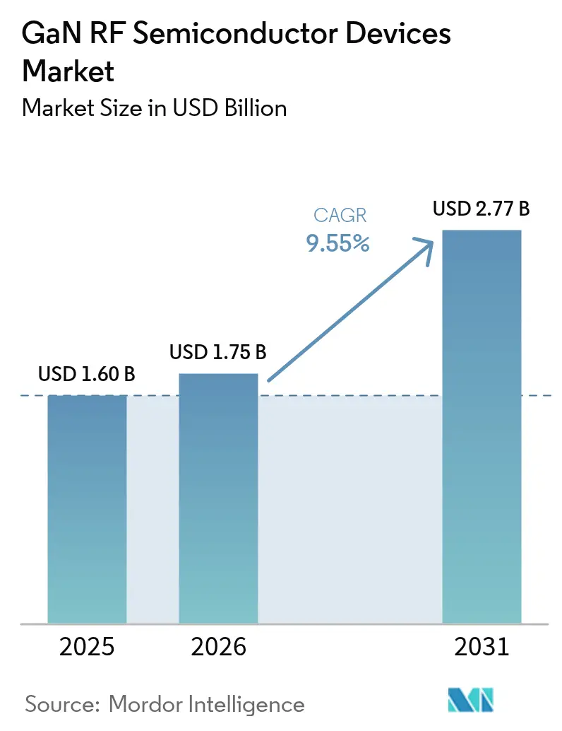
| Market Size (2026) | USD 1.75 Billion |
| Market Size (2031) | USD 2.77 Billion |
| Growth Rate (2026 - 2031) | 9.55 % |
| Fastest Growing Market | Asia Pacific |
| Largest Market | Asia Pacific |
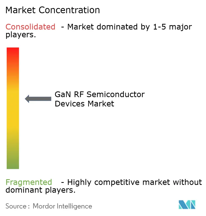
| Market Concentration | Medium |
Major Players
*Disclaimer: Major Players sorted in no particular order Image © Mordor Intelligence. Reuse requires attribution under CC BY 4.0. |
|
GaN RF Semiconductor Devices Market Analysis by Mordor Intelligence
The GaN RF semiconductor devices market size in 2026 is estimated at USD 1.75 billion, growing from 2025 value of USD 1.60 billion with 2031 projections showing USD 2.77 billion, growing at 9.55% CAGR over 2026-2031. Rising demand for high-frequency, high-power solutions in 5G infrastructure, active electronically scanned array (AESA) radar, satellite payloads, and 79 GHz automotive imaging radar positioned gallium nitride as a mainstream technology across telecom, defense, and mobility ecosystems. GaN-on-SiC remained the performance benchmark for thermal robustness, while the transition to 200 mm GaN-on-Si wafers compressed cost gaps versus legacy LDMOS, amplifying adoption in price-sensitive sub-6 GHz radio units. Regionally, the GaN RF semiconductor devices market benefited from Asia-Pacific’s policy-backed semiconductor self-reliance drive and concurrent U.S.–EU defense modernization budgets that prioritized wide-bandgap electronics. Intensifying competition among vertically integrated manufacturers triggered rapid patent filings, strategic acquisitions, and capacity expansions designed to ease 150 mm and 200 mm epi-wafer bottlenecks and secure substrate resilience for emerging mmWave and 6 G research programs.
Key Report Takeaways
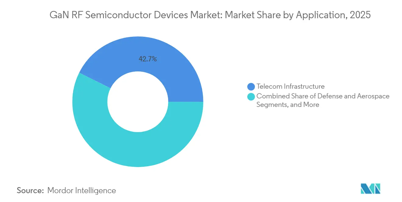
- By application, telecom infrastructure led with 42.65% revenue share in 2025, while automotive is forecast to accelerate at an 17.95% CAGR to 2031.
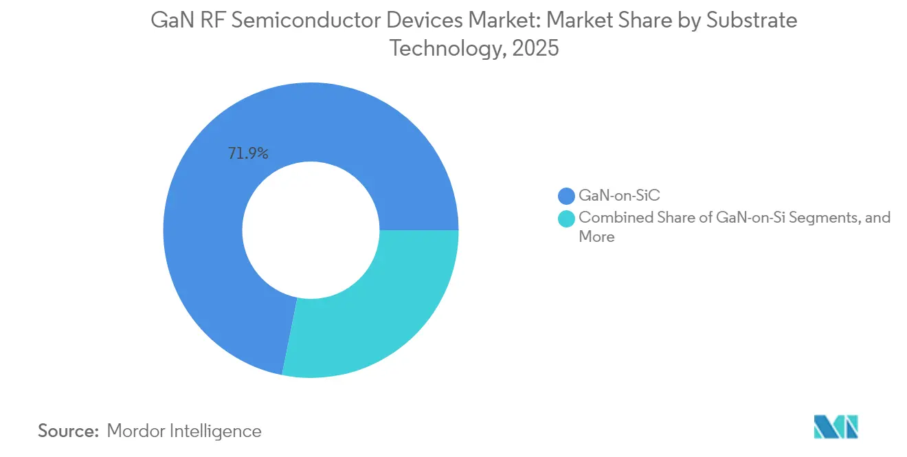
- By substrate technology, GaN-on-SiC held 71.85% of the GaN RF semiconductor devices market share in 2025; GaN-on-Si is projected to expand at a 21.35% CAGR through 2031.
- By frequency band, C/X-Band commanded 33.10% revenue in 2025, whereas the mmWave segment is set to register a 20.95% CAGR during 2026-2031.
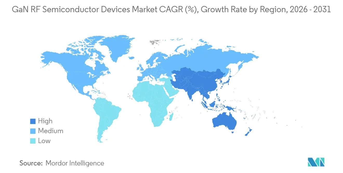
- By geography, Asia-Pacific captured 33.80% of global revenue in 2025 and is expected to post an 17.80% CAGR over the forecast horizon.
- By device type, discrete transistors represented 45.75% share of the GaN RF semiconductor devices market size in 2025; MMIC power amplifiers are poised for a 18.65% CAGR to 2031.
Note: Market size and forecast figures in this report are generated using Mordor Intelligence’s proprietary estimation framework, updated with the latest available data and insights as of 2026.
Market Trends and Insights
Drivers Impact Analysis of GaN RF Semiconductor Devices Market*
| Driver | (~) % Impact on CAGR Forecast | Geographic Relevance | Impact Timeline |
|---|---|---|---|
| 5G Macro- and Small-Cell Roll-outs across Asia-Pacific | +2.8% | Asia-Pacific, with spillover to North America and Europe | Medium term (2-4 years) |
| U.S./EU AESA Radar Modernization Funding | +1.7% | North America, Europe | Long term (≥ 4 years) |
| LEO / MEO Sat-Com Constellation Payload Demand | +1.5% | Global, with a concentration in North America | Medium term (2-4 years) |
| mmWave Automotive Imaging Radar Adoption in China and South Korea | +2.1% | China, Korea, with spillover to Europe | Medium term (2-4 years) |
| High-Power Wireless Charging for Industrie 4.0 Robotics | +0.8% | Europe, North America, Japan | Long term (≥ 4 years) |
| Rapid Proliferation of Open-RAN Remote Radio Heads | +1.2% | Global | Short term (≤ 2 years) |
| Source: Mordor Intelligence | |||
5G macro- and small-cell roll-outs accelerate GaN adoption
Massive-MIMO base-station architectures installed across China, Korea, and Japan relied on up to 64 power-amplifier channels, where gallium nitride delivered a 15-20% energy-efficiency uplift versus LDMOS, cutting site-level operating costs. Open-RAN standardization further decoupled radio hardware from system vendors, enabling specialist GaN suppliers to win sockets for remote-radio-head upgrades. Record deployments by China Mobile validated field reliability, while Qorvo’s 0.013% failure rate reinforced operator confidence.[1]Qorvo, “GaN Innovation Technology,” qorvo.com Progressive reductions in USD/W output through 200 mm wafer migration positioned the GaN RF semiconductor devices market for broader penetration of rural and deep-indoor small-cell layers. Telecom carriers’ energy-saving targets aligned with GaN’s lower heat dissipation, catalyzing procurement frameworks that rewarded efficiency metrics over component price.
U.S./EU AESA radar modernization drives high-power demand
The U.S. Department of Defense elevated GaN to Manufacturing Readiness Level 10 and allocated more than USD 3 billion for next-generation radar programs between 2024-2025, triggering multi-year production ramps for high-power monolithic microwave integrated circuits (MMICs). European ministries mirrored this trajectory through long-range surveillance and electronic-warfare refresh cycles, where GaN’s superior power density increased detection range and jamming effectiveness. Honeywell’s USD 29.9 million contract to retrofit Navy low-band transmitters with GaN exemplified obsolescence mitigation and spectrum agility priorities. Packaging breakthroughs that survived 200 W/mm heat flux migrated downstream to commercial telecom radios, expanding the GaN RF semiconductor devices market beyond defense silos.
LEO/MEO sat-com constellation payload demand
Multi-orbit broadband initiatives require compact, radiation-tolerant RF front-ends capable of multi-band coverage under strict power budgets. TESAT’s 120 W GaN SSPAs in L/S-Band and 60 W versions in C-Band met these constraints and established a template for Ku/Ka-Band upgrades. The replacement of traveling-wave-tube amplifiers with solid-state GaN solutions slashed mass and elevated throughput, prompting a cascade of follow-on orders from new-space operators. Ecosystem players such as EPC Space unveiled rad-hard power management ICs, catalyzing vertically integrated module offerings that widened the GaN RF semiconductor devices market footprint in space infrastructure.
mmWave automotive imaging radar adoption in China and South Korea
Regulatory safety mandates and consumer demand for Level-3+ autonomous features accelerated 79 GHz radar penetration. GaN MMICs enabled 2 cm object resolution at 200 m, allowing OEMs to reduce sensor counts without sacrificing performance, as demonstrated in BMW’s 2025 models. Tier-1 suppliers in Shanghai and Seoul shifted toward GaN front-ends to meet stringent form-factor and thermal budgets, stimulating localized supply-chain investments and reinforcing the GaN RF semiconductor devices market as a strategic node in advanced driver-assistance systems.
Restraints Impact Analysis of GaN RF Semiconductor Devices Market*
| Restraint | (~) % Impact on CAGR Forecast | Geographic Relevance | Impact Timeline |
|---|---|---|---|
| Cost Premium vs. LDMOS in Sub-6 GHz Base-Stations | -1.3% | Global, with higher impact in price-sensitive markets | Short term (≤ 2 years) |
| SiC Encroachment in >3 kW Tactical Radar Blocks | -0.7% | North America, Europe | Medium term (2-4 years) |
| Epi-wafer and Substrate Supply Bottlenecks (150 and 200 mm) | -1.5% | Global | Medium term (2-4 years) |
| Thermal Management and Reliability at >200 W/mm | -0.9% | Global | Long term (≥ 4 years) |
| Source: Mordor Intelligence | |||
Cost premium tempers penetration in price-sensitive deployments
In 2024, GaN power amplifiers carried a 40% price delta over LDMOS for sub-6 GHz radios, delaying transitions in emerging markets, even though energy savings absorbed the gap within 18 months of operation. Texas Instruments’ move to 8-inch GaN-on-Si fabrication lowered die cost by more than 10%, but macroeconomic pressures still constrained carrier capex, especially in India and parts of Southeast Asia. Telecom OEMs, therefore, maintained dual-sourcing strategies, sustaining LDMOS volume and limiting near-term upside for the GaN RF semiconductor devices market.
Epi-wafer and substrate shortages create production chokepoints
Limited 200 mm GaN-on-SiC capacity and longer lead times for high-quality SiC substrates created allocation environments, forcing device vendors to prioritize defense and space contracts. Research fabs documented contamination and bow challenges when scaling GaN-on-Si to 200 mm CMOS lines, delaying yield learning curves. STMicroelectronics’ decision to co-locate GaN epitaxy and panel-level packaging in Italy illustrated vertical-integration responses, yet meaningful capacity relief is unlikely before late 2026, capping short-term supply for the expanding GaN RF semiconductor devices market.
*Our forecasts treat driver/restraint impacts as directional, not additive. The impact forecasts reflect baseline growth, mix effects, and variable interactions.
GaN RF Semiconductor Devices Market Segment Analysis
By Application:
Telecom Infrastructure Sustains Leadership While Automotive SurgesTelecom infrastructure accounted for 42.65% of 2025 revenue, anchoring the GaN RF semiconductor devices market. Base-station vendors adopted GaN to unlock smaller footprints and a 55.2% drain efficiency benchmark in macro radio units. This translates to reduced cooling loads and lower tower-top weight, critical for dense 5G rollouts. Open-RAN disaggregation encouraged independent power-amplifier specialists to capture design wins, while Soitec’s engineered substrates reduced insertion losses, boosting coverage per site. The GaN RF semiconductor devices market retained momentum through 2025 as operators trialed 6 G sub-THz pilots that presupposed GaN front ends.Automotive radar remained a modest slice in 2024 but is forecast to expand at an 17.95% CAGR to 2031. China’s mandatory advanced-driver-assistance mandates and South Korea’s connected-car ecosystem spurred demand for 79 GHz imaging radar, where GaN handled millimeter-wave power density without compromising reliability. V2X communication pilots incorporating GaN PA-LNA modules amplify volume prospects. Cost-down roadmaps tied to 200 mm GaN-on-Si wafers promised alignment with mainstream vehicle electronics, creating scale for the wider GaN RF semiconductor devices market.Across defense and aerospace, radar, electronic warfare, and sat-com payloads drew on GaN’s radiation tolerance and output power. Consumer electronics adopted GaN PAs for Wi-Fi 7 routers and handset front ends, validating smaller-signal opportunities. Industrial robotics embraced 6.78 MHz wireless-charging transmitters powered by GaN HEMTs, underscoring cross-sector breadth that diversified revenue streams.



By Device Type:
Discrete Transistors Dominate as MMIC Integration ClimbsDiscrete power transistors captured 45.75% share in 2025, reflecting entrenched design-in cycles across radar, broadcast, and macro-cell radios. MACOM’s portfolio spanned 2 W to 7 kW, illustrating scalability that underpinned the GaN RF semiconductor devices market. [2]MaxLinear, “MaxLinear and RFHIC Deliver High-Efficiency Power Amplifier,” investors.maxlinear.com Thermal-enhanced bolt-down packages supported >80% drain efficiency, extending device lifetimes in harsh duty cycles.Monolithic microwave integrated-circuit power amplifiers delivered the fastest growth, projected at 18.65% CAGR through 2031. Phased-array modules, space-constrained sat-com terminals, and mmWave backhaul radios favored MMICs that collapsed gain stages and bias networks into compact dies. Qorvo’s wideband QPA2210D exemplified this trend, offering 6 dB higher power-added efficiency versus discrete alternatives. RF switches and front-end modules employed enhancement-mode GaN transistors to handle hot-switching stresses, while low-noise amplifiers began displacing GaAs in C-Band satellite links, broadening the GaN RF semiconductor devices industry landscape.
By Substrate Technology:
GaN-on-SiC Retains the Lead Despite GaN-on-Si MomentumGaN-on-SiC held 71.85% of 2025 revenue owing to 370 W/mK thermal conductivity that enabled >200 W/mm power density in AESA transmit-receive modules. Sumitomo Electric’s 750 W C-Band transistor achieved 80% drain efficiency, validating SiC’s thermal headroom. Lockheed Martin’s fighter-jet radar adoption underscored reliability expectations that kept GaN-on-SiC central to mission-critical deployments within the GaN RF semiconductor devices market.Conversely, GaN-on-Si is set to rise at a 21.35% CAGR, propelled by CMOS compatibility and 200 mm wafer economics that reduced dollar-per-watt metrics. GlobalFoundries and Texas Instruments initiated volume runs in Vermont and Dallas, respectively, shortening learning curves and attracting handset RF front-end projects. The GaN RF semiconductor devices market size for GaN-on-Si segments is forecast to widen as yields surpass 90% and gate-swing ruggedness matches SiC benchmarks.Emerging substrates such as copper-diamond composites introduced 800 W/mK heat-spreading properties for microwave modules exceeding 10 GHz, while GaN-on-Diamond prototypes targeted airborne early-warning radars. Diversification signalled a maturing ecosystem that aligned thermal profiles with application-specific figures of merit.
By Frequency Band:
C/X-Band Dominates, mmWave AcceleratesC/X-Band devices generated 33.10% revenue in 2025, fuelled by naval radar, satellite ground terminals, and 5 G massive-MIMO backhaul. Qorvo’s TGA2578-CP provided 30 W saturated output across 2-6 GHz, reinforcing design loyalty to GaN in this spectrum. Stable program funding cycles insulated demand from macroeconomic wings, giving the GaN RF semiconductor devices market a predictable baseline.mmWave (>40 GHz) components, including 5 G FR2 power amplifiers and E-Band point-to-point links, are projected to post a 20.95% CAGR. MDPI-documented prototypes reached 24 dBm saturated output with 20% PAE across 20-35 GHz, signalling readiness for urban small-cell densification. Ku/Ka-Band served HTS satellite gateways, while L/S-Band and VHF/UHF segments maintained roles in legacy radars and broadcast infrastructure. Broadband GaN PAs capable of 2-18 GHz coverage reduced line-item inventories for integrators, strengthening vendor leverage across the GaN RF semiconductor devices market.
Geography Analysis
APAC GaN RF Semiconductor Devices Market
Asia-Pacific led with 33.80% of 2025 revenue and is projected to advance at an 17.80% CAGR through 2031. China’s 5 G base-station surge, local GaN foundry build-outs, and policy support under the “third semiconductor wave” catalyzed regional self-reliance. Korea focused on AI-centers and automotive radar, while Japan leveraged consumer-electronics legacy and SiC substrate supply. Taiwan’s advanced backend services accelerated GaN-on-Si cost optimization, reinforcing the GaN RF semiconductor devices market growth loop.
North America GaN RF Semiconductor Devices Market
North America ranked second, buoyed by the U.S. defense budget and satellite-internet mega constellations. Government funding for domestic fabs, such as Polar Semiconductor’s Minnesota GaN-on-Si project, supported supply-chain resiliency. Canada’s telecom revamps and Mexico’s automotive-electronics clusters created continental demand diversity that insulated the regional GaN RF semiconductor devices market from single-sector volatility.
Europe GaN RF Semiconductor Devices Market
Europe combined automotive radar leadership with energy-efficient industrial drives. Germany spearheaded 79 GHz vehicle sensor roll-outs, France emphasized aerospace payloads, and the United Kingdom prioritized spectrum-dominated electronic-warfare upgrades. EU strategic autonomy packages channelled grants to joint ventures such as IQE–X-FAB’s 650 V GaN platform, nurturing a localized value chain that underpinned the GaN RF semiconductor devices market size expansion in the bloc.
South America, GCC and Oceania GaN RF Semiconductor Devices Market
Emerging adoption across Brazil, Gulf Cooperation Council smart-city rollouts, and Australia’s low-Earth-orbit backhaul trials showcased the technology’s global diffusion trajectory.

Regulatory Landscape
Regulation affecting GaN RF semiconductor devices is increasingly shaped by spectrum governance and cross-border technology controls, particularly where devices are used in 5G/6G infrastructure and defense-grade RF systems. In the United States, the Department of Commerce Bureau of Industry and Security (BIS) updated Export Administration Regulations in May 2026 to capture specific GaN module implementations. This reflects controls tied to packaging and performance-relevant form factors rather than the material category alone.
BIS guidance issued May 31, 2026 clarified the extraterritorial reach of certain license requirements based on entity headquarters, increasing compliance complexity for global suppliers. Device compliance and certification requirements are also becoming more technical and documentation-heavy, with the U.S. Federal Communications Commission (FCC) adding device-authorization integrity review for industrial RF equipment on June 15, 2026 and raising traceability expectations for GaN-based RF generators and modular transmitter documentation. In Japan, METI initiated a special import review on July 4, 2026 for GaN power modules referencing JEDEC JESD51-14 thermal measurement practices, tying market access to measured thermal performance data rather than simulated results. China introduced a dedicated HS code for GaN power modules and certain SiC MOSFETs in July 2026, increasing customs classification granularity and tightening the documentation needed for compliant cross-border trade.
Value Chain Analysis
The GaN RF semiconductor devices value chain runs from raw materials and substrates (gallium supply, SiC substrates for GaN-on-SiC, and silicon wafers for 200 mm GaN-on-Si), through epitaxial growth (MOCVD), device design (HEMTs, MMIC PAs, front-end modules), and wafer fabrication by IDMs and specialty foundries. It then extends to high-frequency packaging, test, and qualification before distribution to OEMs and integrators serving telecom infrastructure, defense and aerospace, satellite communications, and automotive radar. Vertically integrated players combine substrate, epitaxy, and device processing to manage thermal and reliability requirements, while fabless RF specialists and foundry partners broaden access to process platforms and shorten design-in cycles.
Key constraints remain concentrated in GaN-on-SiC epitaxial capacity, qualified high-frequency packaging, and specialized RF test and burn-in, with long qualification cycles for aerospace and defense programs in particular. Industry responses increasingly include licensing, second-sourcing, and platform partnerships to de-risk supply and expand manufacturing options. For example, EPC announced a strategic GaN technology licensing and second-sourcing agreement with Renesas in February 2026, and GlobalFoundries has highlighted scaling RF GaN toward system-level deployment for wireless infrastructure, pointing to deeper foundry engagement across the RF GaN ecosystem. Export controls and related compliance requirements continue to shape material and device flows, influencing sourcing strategy, lead times, and customer qualification sequencing across regions.
Competitive Landscape
The GaN RF semiconductor devices market exhibited moderate concentration; the top five vendors controlled roughly 60% of revenue, leaving ample room for niche innovators. Wolfspeed, Qorvo, and NXP leveraged cradle-to-package integration, encompassing SiC substrate growth, epitaxy, HEMT design, and advanced thermal packaging. MACOM and Sumitomo Electric focused on high-power transistors, while startups such as Finwave pursued handset-grade GaN-on-Si paths.
Capacity race dynamics shaped 2024-2025 collaboration patterns. WIN Semiconductors’ alliance with Viper RF opened GaN-enabled custom MMIC services, targeting 1-150 GHz coverage.[4]WIN Semiconductors, “Welcomes Viper RF,” fox59.com Infineon qualified 200 mm SiC fabs, expanding projectile into power-electronics adjacency yet sharpening process control skills that cross-pollinated into RF lines. Patent analytics firm Knowmade recorded a Q4 2024 surge in GaN filings, reflecting intensified moat-building activities.
Strategic differentiation hinged on power-added-efficiency roadmaps, thermal management IP, and participation in open reference-design consortia. Data-center operators and automotive OEMs began engaging directly with device makers to align long-term supply and drive custom derivative flows, signaling a shift from component-level competition toward solution-centric engagements that will reshape the GaN RF semiconductor devices market through 2030.
GaN RF Semiconductor Devices Industry Leaders
-
Wolfspeed, Inc.
-
Qorvo, Inc.
-
Sumitomo Electric Device Innovations
-
NXP Semiconductors N.V.
-
MACOM Technology Solutions — GaN-on-SiC
- *Disclaimer: Major Players sorted in no particular order
GaN RF Semiconductor Devices Market Companies Covered in this Report
- Wolfspeed, Inc.
- Qorvo, Inc.
- Sumitomo Electric Device Innovations
- NXP Semiconductors N.V.
- MACOM Technology Solutions — GaN-on-SiC
- Broadcom Inc.
- Infineon Technologies AG
- RFHIC Corp.
- Ampleon Netherlands B.V.
- Mitsubishi Electric Corporation
- Fujitsu Ltd. (GaN RF)
- Northrop Grumman Microelectronics
- Integra Technologies, Inc.
- Analog Devices Inc.
- WIN Semiconductors Corp.
- Finwave Semiconductor Inc.
- Tagore Technology Inc.
- Guerrilla RF
- SEDI – Silent-Solutions Engineering (EU)
- Teledyne e2v HiRel

Market Opportunities and Future Outlook
White space is expanding where system makers need higher integration and tighter SWaP constraints, especially in radar front ends, satellite payloads, and compact infrastructure radios that can use GaN module-level solutions rather than discrete-only designs. A practical signal of this shift is the move toward production-qualified RF GaN process platforms for infrastructure scale-up, including GlobalFoundries communicating production readiness of its 130 nm RF GaN technology (RFGaN1) for high-power wireless infrastructure. Demand signals in GaN-on-Si are also building beyond macro base stations, illustrated by CETC 55th Research Institute reporting more than 5 million units shipped of a mass-produced GaN-on-silicon RF chip for smart-terminal applications.
On the supply side, opportunities center on securing GaN-on-SiC substrates and epi-wafers while narrowing the cost premium that slows adoption in price-sensitive sub-6 GHz deployments. Long-term supply arrangements and upstream investment are becoming more prominent for stabilizing availability for defense and satcom programs, with MACOM reporting a GBP 45 million investment in IQE alongside long-term supply agreements intended to strengthen the GaN-on-SiC supply chain. Trade and IP actions are also changing accessible sourcing options, including a May 2026 U.S. International Trade Commission determination banning certain patent-infringing Innoscience GaN products from the U.S. market, which changes sourcing options for OEMs and increases the value of differentiated process IP and clean-room-proven design flows. Additional headroom appears at higher frequency bands, including W-band millimeter-wave MMICs for advanced backhaul and sensing, where patent mapping indicates room for new architectures and packaging approaches that maintain linearity and thermal margins.
Recent Industry Developments in GaN RF Semiconductor Devices Market
- July 2026: Wolfspeed filed a patent infringement lawsuit against Navitas Semiconductor in the U.S. District Court for the District of Delaware, asserting infringement tied to its GaN and SiC patent portfolio. The action highlights the growing importance of defensible IP in wide-bandgap device roadmaps and can affect second-sourcing choices for OEMs that rely on stable, litigations-free supply chains.
- June 2026: Qorvo introduced the QPF5012 X-band radar front-end module, targeting compact radar architectures with 10 W transmit power and 42% power-added efficiency. The rollout supports the broader move toward integrated GaN RF modules for AESA and other defense systems, where size, weight, power, and sensitivity constraints shape component selection.
- June 2024: Qorvo launched compact high-power Ku-band GaN MMIC amplifiers aimed at satellite communications payloads and terminals. This expanded the set of space-qualified, high-frequency power solutions and reinforced the migration from traveling-wave-tube and legacy solid-state approaches toward GaN-based SSPAs and integrated RF front ends.


GaN RF Semiconductor Devices Market Report Scope and Research Methodology
Market Definition and Coverage
For this methodology, the market covers revenue generated from GaN-based RF semiconductor devices used to amplify, switch, or condition RF signals in end equipment like telecom infrastructure, radar, and satellite systems.
Scope exclusions: This sizing excludes non-GaN RF technologies and does not count downstream system integration and installation services.
Segments Covered in This Report
-
By Application
- Defense and Aerospace
- Telecom Infrastructure
- Consumer Electronics
- Automotive (ADAS, V2X)
- Industrial and Energy
- Data Centers and High-Efficiency Power Links
-
By Device Type
- Discrete RF Power Transistors
- MMIC / Monolithic Power Amplifiers
- RF Switches and Front-End Modules
- Low-Noise and Driver Amplifiers
-
By Substrate Technology
- GaN-on-SiC
- GaN-on-Si
- GaN-on-Diamond and Advanced Composites
-
By Frequency Band
- VHF / UHF (<1 GHz)
- L / S-Band (1-4 GHz)
- C / X-Band (4-12 GHz)
- Ku / Ka-Band (12-40 GHz)
- mmWave (›40 GHz, incl. 5G FR2)
-
By Geography
-
North America
- United States
- Canada
- Mexico
-
South America
- Brazil
- Argentina
- Rest of South America
-
Europe
- Germany
- United Kingdom
- France
- Italy
- Spain
- Rest of Europe
-
Asia-Pacific
- China
- Japan
- South Korea
- India
- Taiwan
- Rest of Asia-Pacific
-
Middle East and Africa
-
Middle East
- Saudi Arabia
- United Arab Emirates
- Turkey
- Rest of Middle East
-
Africa
- South Africa
- Rest of Africa
-
Middle East
-
North America
Data Sources, Market Sizing, and Validation
Desk Research
Desk research was used to set the outer limits of demand and to avoid building the model from assumptions alone. We referred to public sources such as semiconductor trade and production statistics from government portals, telecom network deployment releases from regulators, defense procurement and budget documents, and standards and spectrum information from bodies such as the ITU and FCC.
Along with that, we reviewed company annual reports, investor decks, and technical notes that explain RF power device performance and adoption (for example around GaN-on-SiC and GaN-on-Si trends). Patent databases were used to track where design activity is rising in RF front ends, and an import export shipment-level database was used selectively to sanity-check cross-border flows of relevant electronic components. These desk sources are illustrative only, and many other public references were also used to collect data, validate it, and clarify open questions.
Primary Interviews and Surveys
Primary interviews and short surveys were completed with people from device supply, RF module and subsystem design, telecom and aerospace demand planning, and distribution channels, so the assumptions could be adjusted to real shipment and pricing behavior. We covered major consuming regions, and then used follow-up calls when responses disagreed on items like average selling price movement, mix shifts between discrete and integrated parts, and timing of defense and telecom programs.
Distribution of primary research fieldwork respondents
| Company type | Respondent position | Region |
|---|---|---|
| Top tier: 34% | CXOs: 15% | APAC: 43% |
| Mid tier: 50% | Functional/Unit leaders: 38% | EMEA: 37% |
| Smaller Players: 16% | Managers: 47% | Americas: 20% |
Market-Sizing & Forecasting
Sizing starts with a top-down build where telecom and defense RF demand pools are reconstructed using deployment and upgrade activity, and then translated into device demand through penetration and content-per-system assumptions. The model uses market fingerprints such as 5G macro and small-cell rollout pace, radar and satellite program timing, substrate mix (GaN-on-SiC versus GaN-on-Si), device mix across discrete parts and MMIC or power amplifier configurations, and typical RF ASP progression by performance tier.
To keep totals realistic, we corroborated the top-down output with selective bottom-up checks, such as sampled ASP multiplied by estimated unit volumes for key use cases, and channel checks on shortages or inventory corrections. When a bottom-up view was incomplete for smaller applications, the missing pieces were handled through ratio-based allocations anchored to the larger, better-evidenced demand signals.
Forecasting is done using scenario analysis supported by simple multivariate relationships, where the key drivers are telecom capex cycles, defense and space procurement visibility, and expected pricing changes as wafer sizes and manufacturing scale evolve. Final growth paths are adjusted after primary feedback confirms whether assumptions like mix shift and design-win timing are happening in the expected years.
Data Validation & Update Cycle
Outputs are cross-checked against independent signals, which include regional deployment metrics, public program awards, and supplier commentary on order flow and utilization. We run variance checks at the region and application level, and then unusual jumps are reviewed by another analyst before sign-off.
Reports are refreshed annually, and interim updates are made when material events occur, such as large defense awards, major fab capacity moves, or sharp pricing shifts. Before delivery, a fresh pass is completed so the latest disclosures and market signals are reflected in the final numbers.
Mordor Intelligence's Gan Rf Semiconductor Devices Market Size Compared With Other Published Estimates
Published market values for GaN RF semiconductor devices can look far apart, even when they all sound like they are studying the same topic. This usually happens because each publisher draws the line differently on what devices count, what year is treated as the base, and how fast prices and adoption are assumed to move.
The main gap comes from whether estimates roll adjacent power categories and broad GaN device revenue into the total, and how they treat device types like discrete RF transistors versus MMIC and front-end modules, which is where Mordor Intelligence applies a device-only revenue scope and then validates ASP and mix through interviews before finalizing the total.
Benchmark comparison
| Source | Market Size | Gaps in Research Methodology |
|---|---|---|
| Mordor Intelligence | USD 1.75 B (2026) | |
| Industry Publisher A | USD 1.43 B (2024) | Uses an earlier base year and a wider application view that can blend RF devices with adjacent power-electronics demand, which changes the revenue pool and lifts long-range growth rates. |
| Industry Publisher B | USD 1.70 B (2024) | Frames the market as RF GaN broadly and emphasizes discrete versus integrated splits, so module and end-use treatment can differ from a device-only scope, and currency timing and ASP paths can be handled differently. |
The table shows that the spread is driven less by math and more by scope and timing choices, especially around what products are counted and what base year anchors the model. By keeping inputs tied to clear demand drivers like telecom rollouts, radar and satellite programs, and realistic ASP movement, the final number stays traceable and repeatable when assumptions are revisited.


Key Questions Answered in the Report
What was the GaN RF semiconductor devices market size in 2026?
The GaN RF semiconductor devices market size reached USD 1.75 billion in 2026.
Which application segment held the largest share in 2025?
Telecom infrastructure commanded 42.65% of 2025 revenue due to rapid 5 G macro- and small-cell deployments.
Why is GaN-on-SiC still dominant despite cost advantages of GaN-on-Si?
GaN-on-SiC offers superior thermal conductivity, supporting >200 W/mm power density required in defense radar and high-power base stations.
Which region will grow the fastest through 2031?
Asia-Pacific is projected to register an 17.80% CAGR, driven by extensive 5 G roll-outs and semiconductor self-reliance initiatives.
How are cost barriers being addressed?
Migration to 200 mm GaN-on-Si wafers and process yield improvements have lowered die cost by more than 10%, narrowing the price gap with LDMOS.
What is driving the surge in mmWave GaN devices?
Expansion of 5 G FR2 networks and early 6 G research requires high-efficiency power amplifiers that can handle propagation losses at >40 GHz, an area where GaN excels.
Page last updated on: