FinFET Technology Market Size and Share
Market Overview
| Study Period | 2019 - 2030 |
|---|---|
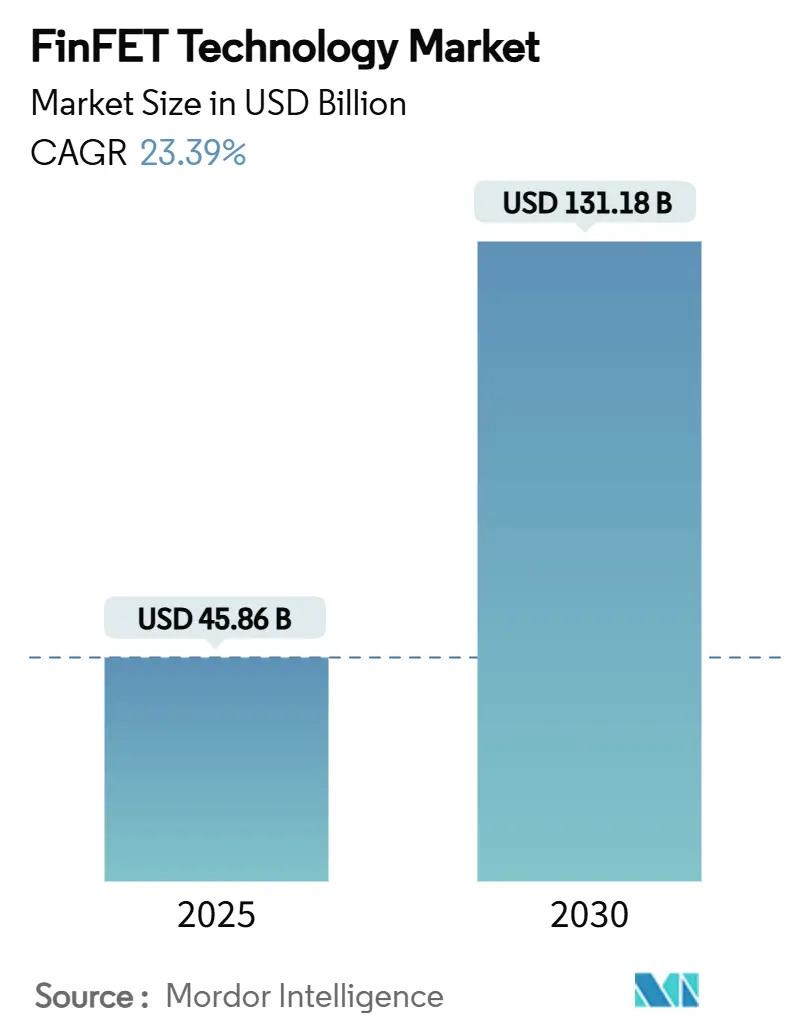
| Market Size (2025) | USD 45.86 Billion |
| Market Size (2030) | USD 131.18 Billion |
| Growth Rate (2025 - 2030) | 23.39% CAGR |
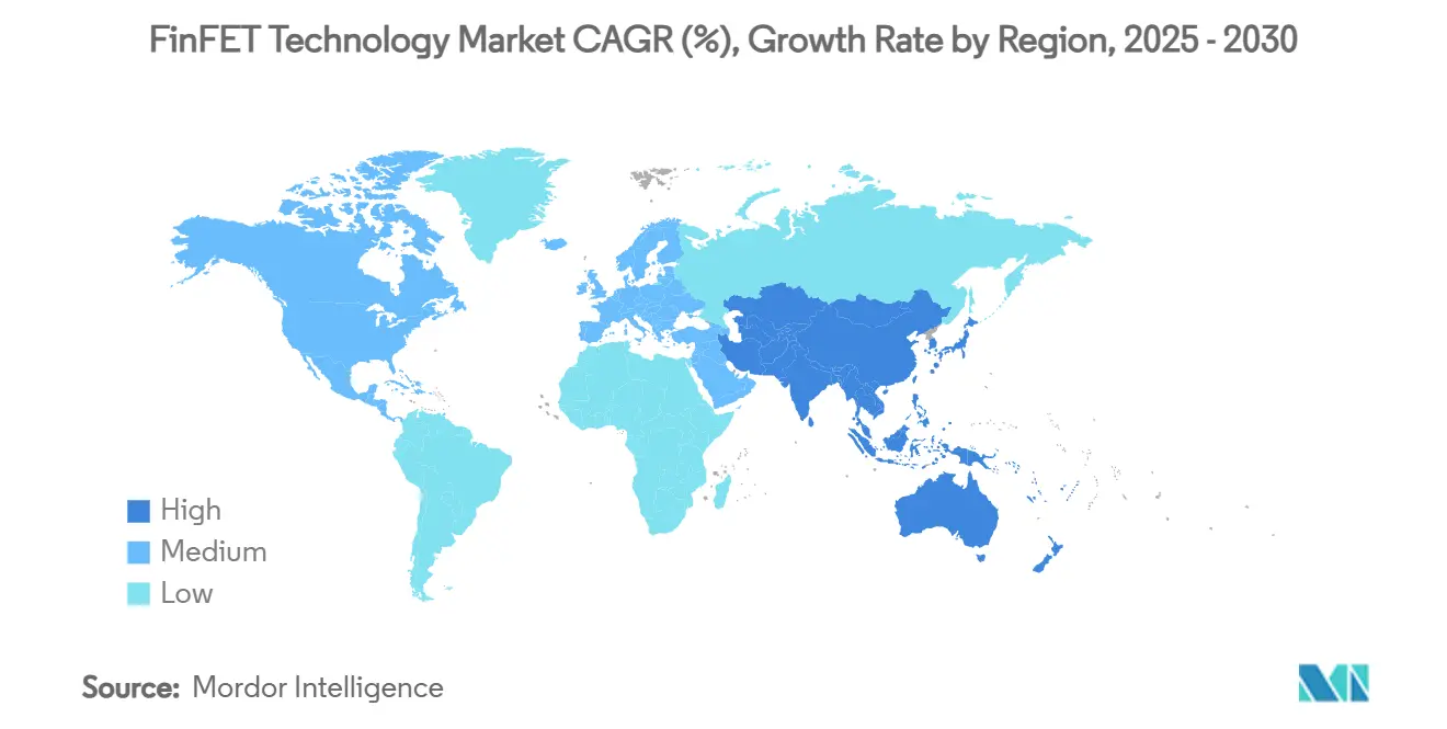
| Fastest Growing Market | Asia Pacific |
| Largest Market | Asia Pacific |
| Market Concentration | High |
Major Players *Disclaimer: Major Players sorted in no particular order Image © Mordor Intelligence. Reuse requires attribution under CC BY 4.0. | |
FinFET Technology Market Analysis by Mordor Intelligence
The FinFET technology market size reached USD 45.86 billion in 2025 and is projected to climb to USD 131.18 billion by 2030, registering a 23.39% CAGR over the forecast period. This rapid expansion is underpinned by the semiconductor sector’s migration to advanced nodes as planar CMOS falls short below the 20 nm threshold. Intensifying compute demand from artificial intelligence, 5G infrastructure, and electric vehicles is concentrating capital on sub-5 nm processes where FinFET devices deliver the required power-performance balance. Subsidy-backed capacity expansions in the United States and European Union are reshaping the geographic footprint of the FinFET technology market, while persistent yield hurdles at the bleeding edge underscore the importance of manufacturing maturity. Simultaneously, heterogeneous integration trends—most notably 3D-IC and chiplet architectures—are multiplying die-level demand for high-performance FinFET wafers.
Key Report Takeaways
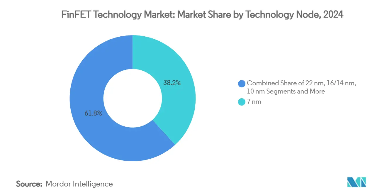
- By technology node, the 7 nm family led with 38.2% of the FinFET technology market share in 2024, while the 5 nm-and-below class is forecast to advance at a 24.2% CAGR through 2030.
- By business model, pure-play foundries controlled 48.6% revenue share in 2024; the IDM segment is expected to post the fastest 25.4% CAGR to 2030.
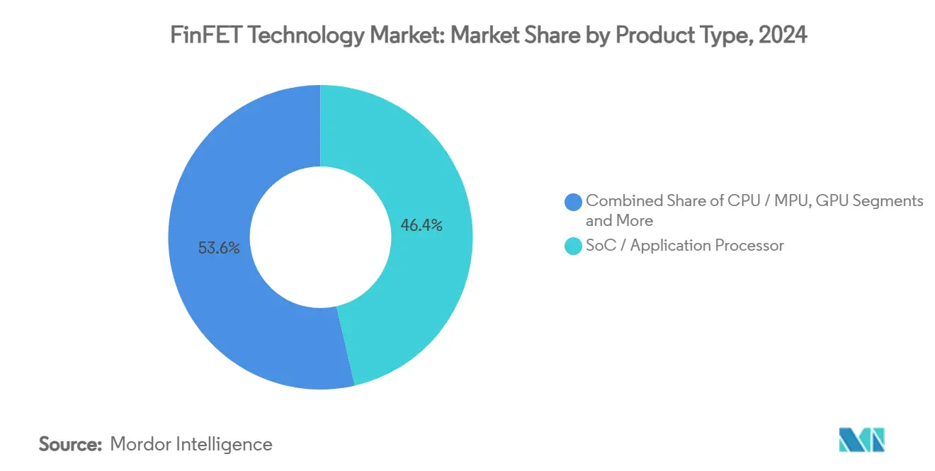
- By product type, system-on-chips and application processors accounted for 46.4% of the FinFET technology market size in 2024, whereas ASIC/accelerators are projected to grow at a 25.6% CAGR.
- By application, smartphones and tablets held a 54.2% share of the FinFET technology market size in 2024, while high-performance computing/data-center devices are expanding at a 24.3% CAGR to 2030.
- By geography, Asia-Pacific captured 61.3% of the FinFET technology market share in 2024 and is anticipated to maintain the fastest 23.8% CAGR through 2030.
Global FinFET Technology Market Trends and Insights
Drivers Impact Analysis*
| Driver | (~) % Impact on CAGR Forecast | Geographic Relevance | Impact Timeline |
|---|---|---|---|
| Explosive 5G/AI-chip demand | +8.2% | Asia-Pacific, North America | Medium term (2-4 years) |
| Transition from planar CMOS below 20 nm | +6.1% | Taiwan, South Korea, global advanced foundries | Long term (≥ 4 years) |
| Automotive ADAS and EV compute surge | +4.7% | Europe, North America, China | Medium term (2-4 years) |
| EU/US CHIPS-Act capacity subsidies | +3.9% | United States, European Union | Long term (≥ 4 years) |
| 3D-IC and advanced packaging pull-through | +3.2% | Asia-Pacific core, spillover to United States and Europe | Medium term (2-4 years) |
| Foundry race for sub-5 nm leadership | +2.8% | Taiwan, South Korea, United States | Short term (≤ 2 years) |
| Source: Mordor Intelligence | |||
Explosive 5G/AI-Chip Demand
Global roll-outs of 5G radios and cloud AI inference engines require logic devices that maximize throughput per watt. Advanced node FinFET processors now dominate high-performance graphics units, dedicated AI accelerators, and custom cloud ASICs, with hyperscale operators signing multi-year wafer agreements to secure capacity. Leading foundries have therefore allocated the majority of their sub-5 nm lines to AI-centric designs, driving tighter cycle times and iterative stepping. The trend is amplified by the rapid adoption of large-language-model workloads that demand trillions of parameters, translating to higher die sizes and elevated transistor counts. As a result, FinFET wafer demand is forecast to accelerate through 2027 before nanosheet transitions gain volume traction. [1]Taiwan Semiconductor Manufacturing Company, “TSMC Arizona and U.S. Department of Commerce Announce up to US$6.6 Billion in Proposed CHIPS Act Direct Funding,” pr.tsmc.com
Transition from Planar CMOS Below 20 nm
Short-channel effects, off-state leakage, and variability rendered two-dimensional transistors impractical beyond the 20 nm node. FinFET’s tri-gate topology restores electrostatic control, enabling threshold voltage scaling alongside gate length reduction. Consequently, nearly every advanced-logic road-map since 2016 has pivoted to FinFET, with bulk and SOI variants delivering steady node-over-node benefits. The coming 2 nm generation will usher in gate-all-around nanosheets, but FinFET remains the volume backbone through 2026 as tool chains, IP libraries, and manufacturing recipes mature. Design houses continue to tape-out FinFET derivatives for risk mitigation until nanosheet yields converge with incumbent 3 nm baselines. [2]Applied Materials, “Gate-All-Around,” appliedmaterials.com
Automotive ADAS and EV Compute Surge
Software-defined vehicles are transforming in-car electronics from distributed microcontrollers to centralized domain computers that rival data-center servers in raw operations per second. Level-3 and higher autonomy stacks require 1,000+ TOPS, mandating advanced FinFET SoCs and dedicated neural-network accelerators. Automotive qualification standards such as AEC-Q100 and ASIL-D favor node-proven FinFET platforms with established reliability. Leading suppliers have introduced 16 nm FinFET microcontrollers featuring embedded MRAM to meet fast write-latency targets, while high-end ADAS processors on 5 nm lines are sampling with OEMs.
EU/US CHIPS-Act Capacity Subsidies
Sovereign concerns over supply-chain concentration have spurred industrial policies offering direct grants, tax credits, and loan guarantees. The United States earmarked USD 39 billion for fabrication grants and an additional USD 75 billion in loan authority, prompting leading foundries to commit multi-fab campuses in Arizona, Ohio, and New York. The European Union’s EUR 43 billion initiative targets a 20% share of global semiconductor manufacturing by 2030, catalyzing a wave of joint ventures focused on automotive and industrial FinFET nodes. These incentives lower initial capital outlays, shorten payback periods, and diversify the customer base, thereby sustaining the FinFET technology market even as node migration costs escalate. [3]Center for Strategic and International Studies, “Tracking CHIPS Act Incentives,” csis.org
Restraints Impact Analysis*
| Restraint | (~) % Impact on CAGR Forecast | Geographic Relevance | Impact Timeline |
|---|---|---|---|
| Rising sub-10 nm capex (> USD 20 billion/fab) | -4.3% | Global | Long term (≥ 4 years) |
| EUV tool supply bottlenecks | -3.1% | Global | Short term (≤ 2 years) |
| Design-rule and EDA complexity spike | -2.7% | Design-intensive regions worldwide | Medium term (2-4 years) |
| Yield variability in multi-foundry flows | -1.9% | Asia-Pacific and emerging foundry geographies | Medium term (2-4 years) |
| Source: Mordor Intelligence | |||
Rising Sub-10 nm Capex
The all-in cost of a greenfield sub-5 nm fab now exceeds USD 25 billion once EUV scanners, high-current implantation, and advanced litho-track clusters are included. Depreciation alone can account for more than 55% of finished-wafer cost, squeezing margins for new entrants and raising the minimum efficient scale. Governments are offsetting part of the burden via grants and tax incentives, yet balance-sheet risks remain elevated, limiting competitive diversity to a small cohort of mega-foundries.[4]SEMI, “300 mm Fab Equipment Spending Forecast to Reach Record USD 137 Billion in 2027,” semi.org
EUV Tool Supply Bottlenecks
Extreme ultraviolet scanners weigh over 150 tonnes, integrate 100,000+ parts, and sell for roughly USD 350 million each. The sole supplier’s annual output is capped by optics polishing, vacuum-chamber machining, and pellicle availability. Queue times stretch beyond 18 months, constraining capacity ramps for both FinFET and upcoming nanosheet nodes. Any disruption—from geopolitical export restrictions to component shortages—immediately cascades through advanced-logic supply chains.
*Our forecasts treat driver/restraint impacts as directional, not additive. The impact forecasts reflect baseline growth, mix effects, and variable interactions.
Segment Analysis
By Technology Node: Sub-5 nm Drives Premium Economics
The 7 nm class commanded 38.2% of the FinFET technology market share in 2024 due to its balance of maturity and performance. Strong tape-out pipelines for flagship handsets, AI accelerators, and automotive domain controllers keep fab loading rates high. Meanwhile, sub-5 nm nodes, including 5 nm and the first-generation 3 nm FinFET processes, recorded the highest uptake trajectory, projected to deliver a 24.2% CAGR by 2030 as cloud providers and automakers migrate workloads toward lower power envelopes. FinFET technology market size contributions from 16/14 nm remain material in cost-sensitive segments, whereas 22 nm mainly serves legacy applications.
Node evolution illustrates a looming architectural pivot: at the 2 nm waypoint, nanosheet transistors take over mainstream production, yet FinFET will coexist for derivative performance-optimized versions until yields equalize. Design houses hedge risk by qualifying both form factors, ensuring continuity for high-volume parts. The bifurcation between ultimate performance requirements and price-sensitive products keeps 10 nm in a demand trough, with customers either staying on 16 nm for cost or leaping to 7 nm for performance gains.


By Foundry Business Model: Pure-Play Stays in Front While IDMs Re-Emerge
Pure-play specialists retained 48.6% revenue share in 2024 as their scale advantages, customer neutrality, and R&D intensity made them the first choice for leading-edge tape-outs. The FinFET technology market size generated by pure-plays benefits from dense customer portfolios across mobile, HPC, and automotive verticals. Nevertheless, integrated device manufacturers are mounting a comeback, forecasting the fastest 25.4% CAGR by leveraging vertical design-to-manufacture control and secure domestic supply chains prioritized by government funding.
This resurgence is most apparent in the United States, where leading IDMs have revamped road maps around ribbon-FET and backside power topologies while simultaneously opening foundry lines to external customers. The fab-lite camp continues to focus on specialized analog-mixed-signal or RF processes, outsourcing the bulk of digital logic to pure-plays. Over time, geopolitical incentives could steer additional volume toward IDMs, but the capital intensity barrier preserves pure-play dominance in the highest-shrinking geometry segments.
By Product Type: AI-Centric ASICs Outpace General-Purpose Devices
System-on-chips and application processors constituted 46.4% of 2024 revenue, reflecting smartphones and consumer electronics. Custom ASIC/accelerators, however, are the fastest-growing slice, projected to rise at 25.6% CAGR as hyperscale operators, automakers, and industrial OEMs redesign workloads for domain-specific silicon. The FinFET technology market size associated with GPU cores remains resilient thanks to AI training demand, but general-purpose CPU sockets face substitution from ARM-based architectures and specialist inferencing chips.
Edge-tier FPGAs fabricated on FinFET nodes are crossing over from prototyping use to production deployments, spurred by configurable logic’s low-latency advantages. Meanwhile, nascent categories such as neuromorphic co-processors rely on FinFET peripherals for control and I/O even when their compute cores adopt alternative device structures. The diversity of product requirements underscores the flexibility of FinFET libraries in balancing power, speed, and leakage across workloads.
By Application: HPC/Data-Center Accelerates Most Rapidly
Smartphones and tablets delivered 54.2% of 2024 shipments, underscoring mobile SoCs’ entrenched dependence on FinFET for battery-life gains. High-performance computing and data-center accelerators now represent the fastest-expanding end-market, with a 24.3% CAGR outlook through 2030 as AI inference and training clusters proliferate. Automotive electronics usage is climbing sharply, anchored by centralized compute stacks that merge infotainment and ADAS functions into 5 nm or 7 nm FinFET processors qualified for ISO 26262 safety levels.
IoT and edge devices open incremental volumes for mature FinFET nodes, where energy efficiency trumps absolute transistor density. Traditional PC and server CPUs are ceding share to accelerator-rich heterogeneous systems, but still consume healthy wafer volumes during generational refresh cycles. Altogether, application segmentation highlights a shift toward data-intensive, latency-sensitive domains that value FinFET’s electrostatic integrity and power efficiency.
Geography Analysis
Asia-Pacific dominated with 61.3% share of the FinFET technology market in 2024, anchored by Taiwan’s extensive foundry network, South Korea’s dual logic-memory capability and China’s ongoing domestic expansion. The region’s 23.8% forecast CAGR reflects continued capital deployment into sub-5 nm lines and advanced packaging facilities. Taiwan alone maintains well over half of global leading-edge capacity, though diversification programs are steering incremental modules to Japan and Singapore for resilience.
North America represents the fastest-growing developed cluster, propelled by CHIPS Act incentives that underwrite greenfield fabs in Arizona, Ohio, and upstate New York. Projected regional share is set to climb from roughly 10% in 2024 to 14% by the early 2030s. Domestic design-to-manufacture loops shorten time-to-market for U.S. cloud and defense customers, while Mexico strengthens its role in assembly-test to leverage USMCA duty advantages.
Europe pursues strategic autonomy with a EUR 43 billion funding envelope that lures joint ventures focused on automotive and industrial FinFET nodes. A landmark German facility, co-sponsored by a Taiwanese foundry leader and local carmakers, will supply 16/12 nm wafers optimized for functional safety. Structural hurdles—talent scarcity and fragmented permitting—could temper the EU’s 20% production share ambition, yet region-specific end-markets guarantee stable pull for qualified FinFET capacity.

Competitive Landscape
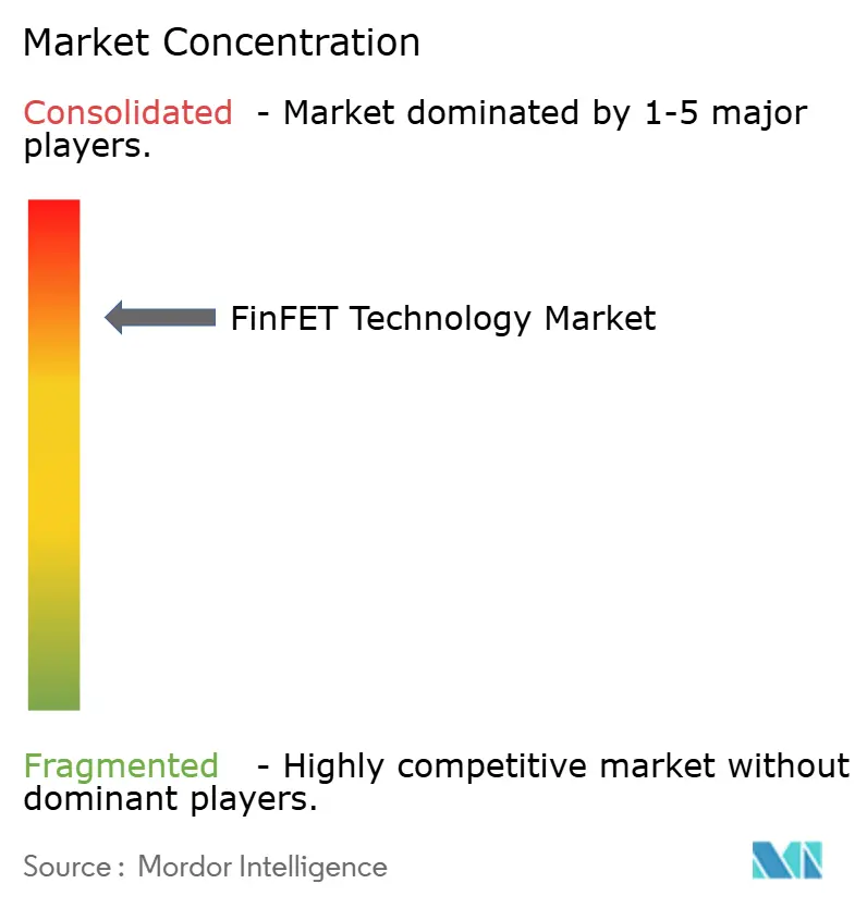
The FinFET technology market is highly concentrated: the largest pure-play foundry accounts for nearly two-thirds of advanced-logic wafer revenue, while the second-ranked supplier holds under 10% and the third is still ramping yield. Escalating capex requirements beyond USD 20 billion per new fab effectively bar late entrants, reinforcing an oligopolistic structure. Leading competitors differentiate via process-design co-optimization, customized transistor libraries and advanced packaging road-maps that bundle logic with high-bandwidth memory.
Recent process milestones include 3 nm FinFET volume ramps achieving high-single-digit defect densities and 2 nm nanosheet risk starts with above-70% yield targets. The market leader has disclosed backside power delivery and nano-flex channel width modulation for its second-generation GAA platform, while a rival emphasizes early High-NA lithography adoption to leapfrog performance metrics. Strategic partnerships between foundries and IP vendors—such as Arm CPU core co-development or EDA tool qualification—further lock in customer ecosystems.
Government incentives tilt competitive positioning. U.S. grants reward domestic tool localization and secure-supply mandates, benefitting IDMs that align with defense procurement. European funding prioritizes automotive reliability enhancements, allowing regional suppliers to capture safety-critical sub-segments. In Asia-Pacific, tax credits and infrastructure co-investment keep operating costs low, ensuring the region retains the largest slice of FinFET technology market size despite reshoring trends elsewhere.
FinFET Technology Industry Leaders
TSMC Limited
Samsung Electronics Co., Ltd.
Intel Corporation
GlobalFoundries Inc.
Semiconductor Manufacturing International Corporation (SMIC)
- *Disclaimer: Major Players sorted in no particular order

Recent Industry Developments
- July 2025: TSMC achieved 90% yield in 2 nm memory chip production, clearing the path for high-volume nanosheet ramp-up.
- July 2025: ASML shipped its first High-NA EUV EXE:5200 scanner to Intel, kick-starting 14 Å node development for 2027 launch.
- April 2025: TSMC unveiled the A14 (1.4 nm-class) platform featuring second-generation nanosheets and NanoFlex Pro channels, targeting mass production in 2028.
- April 2025: Synopsys and Intel Foundry launched full-flow EDA support for 18A and 18A-P processes, streamlining customer transition to ribbon-FET and backside power nodes.


Global FinFET Technology Market Report Scope
| 22 nm |
| 16/14 nm |
| 10 nm |
| 7 nm |
| 5 nm and Below |
| Pure-play Foundry |
| IDM |
| Fab-Lite |
| CPU / MPU |
| GPU |
| SoC / Application Processor |
| FPGA |
| ASIC / Accelerator |
| Others |
| Smartphones and Tablets |
| High-Performance Computing / Data Center |
| Automotive Electronics |
| IoT / Edge Devices |
| Others |
| North America | United States | |
| Canada | ||
| Mexico | ||
| South America | Brazil | |
| Argentina | ||
| Rest of South America | ||
| Europe | Germany | |
| United Kingdom | ||
| France | ||
| Italy | ||
| Russia | ||
| Spain | ||
| Rest of Europe | ||
| Asia-Pacific | China | |
| Japan | ||
| South Korea | ||
| Taiwan | ||
| India | ||
| Rest of Asia-Pacific | ||
| Middle East and Africa | Middle East | Saudi Arabia |
| United Arab Emirates | ||
| Turkey | ||
| Rest of Middle East | ||
| Africa | South Africa | |
| Egypt | ||
| Rest of Africa | ||
| By Technology Node | 22 nm | ||
| 16/14 nm | |||
| 10 nm | |||
| 7 nm | |||
| 5 nm and Below | |||
| By Foundry Business Model | Pure-play Foundry | ||
| IDM | |||
| Fab-Lite | |||
| By Product Type | CPU / MPU | ||
| GPU | |||
| SoC / Application Processor | |||
| FPGA | |||
| ASIC / Accelerator | |||
| Others | |||
| By Application | Smartphones and Tablets | ||
| High-Performance Computing / Data Center | |||
| Automotive Electronics | |||
| IoT / Edge Devices | |||
| Others | |||
| By Geography | North America | United States | |
| Canada | |||
| Mexico | |||
| South America | Brazil | ||
| Argentina | |||
| Rest of South America | |||
| Europe | Germany | ||
| United Kingdom | |||
| France | |||
| Italy | |||
| Russia | |||
| Spain | |||
| Rest of Europe | |||
| Asia-Pacific | China | ||
| Japan | |||
| South Korea | |||
| Taiwan | |||
| India | |||
| Rest of Asia-Pacific | |||
| Middle East and Africa | Middle East | Saudi Arabia | |
| United Arab Emirates | |||
| Turkey | |||
| Rest of Middle East | |||
| Africa | South Africa | ||
| Egypt | |||
| Rest of Africa | |||


Key Questions Answered in the Report
What is driving the rapid growth of the FinFET technology market?
Surging AI workloads, 5G device proliferation and electrification in vehicles are forcing designers to adopt sub-5 nm FinFET nodes that offer superior power efficiency and speed, resulting in a 23.39% CAGR through 2030.
How large will the FinFET technology market be by 2030?
The FinFET technology market size is forecast to reach USD 131.18 billion by 2030, nearly triple its 2025 value.
Which technology node will dominate FinFET revenues during the forecast period?
The 7 nm family currently holds the largest revenue share, but 5 nm-and-below nodes are set to grow the fastest at a 24.2% CAGR as AI and HPC demand accelerate.
Why are government subsidies important for FinFET capacity expansion?
With each new sub-5 nm fab costing more than USD 20 billion, grants and tax credits under the U.S. and EU CHIPS Acts lower capital risk, enabling geographically diversified manufacturing.
Who are the leading players in the FinFET foundry space?
A single Taiwan-based pure-play foundry holds roughly two-thirds of advanced-logic revenue, followed by a South Korean conglomerate and a U.S. IDM pursuing aggressive capacity ramps.
When will gate-all-around devices replace FinFET at scale?
Commercial 2 nm nanosheet production begins in 2025, but mainstream volumes will coexist with FinFET nodes until yields, tool readiness and IP ecosystems converge—likely after 2027.
Page last updated on:


