Gate-all-Around FET Market Size and Share
Market Overview
| Study Period | 2019 - 2030 |
|---|---|
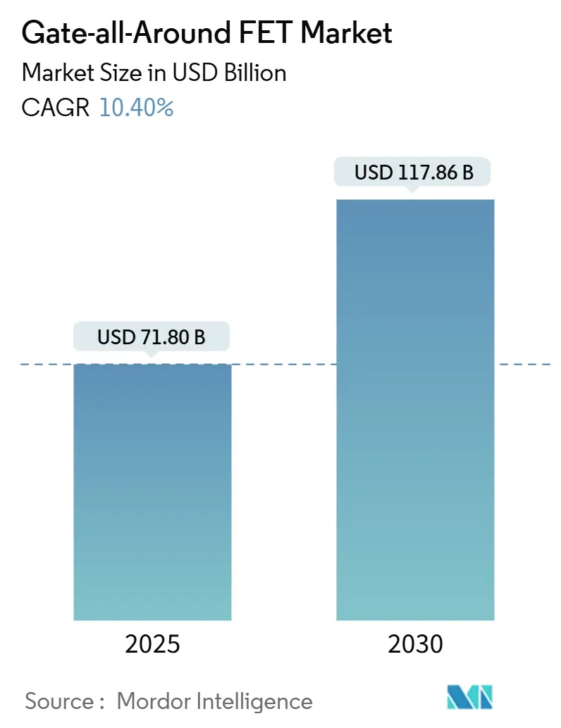
| Market Size (2025) | USD 71.80 Billion |
| Market Size (2030) | USD 117.86 Billion |
| Growth Rate (2025 - 2030) | 10.40% CAGR |
| Fastest Growing Market | Asia Pacific |
| Largest Market | Asia Pacific |
| Market Concentration | High |
Major Players *Disclaimer: Major Players sorted in no particular order Image © Mordor Intelligence. Reuse requires attribution under CC BY 4.0. | |
Gate-all-Around FET Market Analysis by Mordor Intelligence
The Gate-all-Around FET (GAAFET) market size stands at USD 71.8 billion in 2025 and is projected to advance to USD 117.86 billion by 2030, reflecting a 10.40% CAGR. This uptrend is driven by the semiconductor industry’s pivot away from FinFET designs that struggle below the 3 nm node, by the immediate need to curb power consumption for artificial intelligence and 5G workloads, and by the proven ability of Gate-all-Around architectures to secure tighter electrostatic control at atomic dimensions. Robust government incentives for advanced fabrication, greater adoption of backside power-delivery networks, and growing high-density design activity at fabless companies further underpin market momentum. Competitive intensity centers on yield gains, cost curves, and rapid design enablement, and first movers are capturing early design wins that translate into long-term volume commitments.
Key Report Takeaways
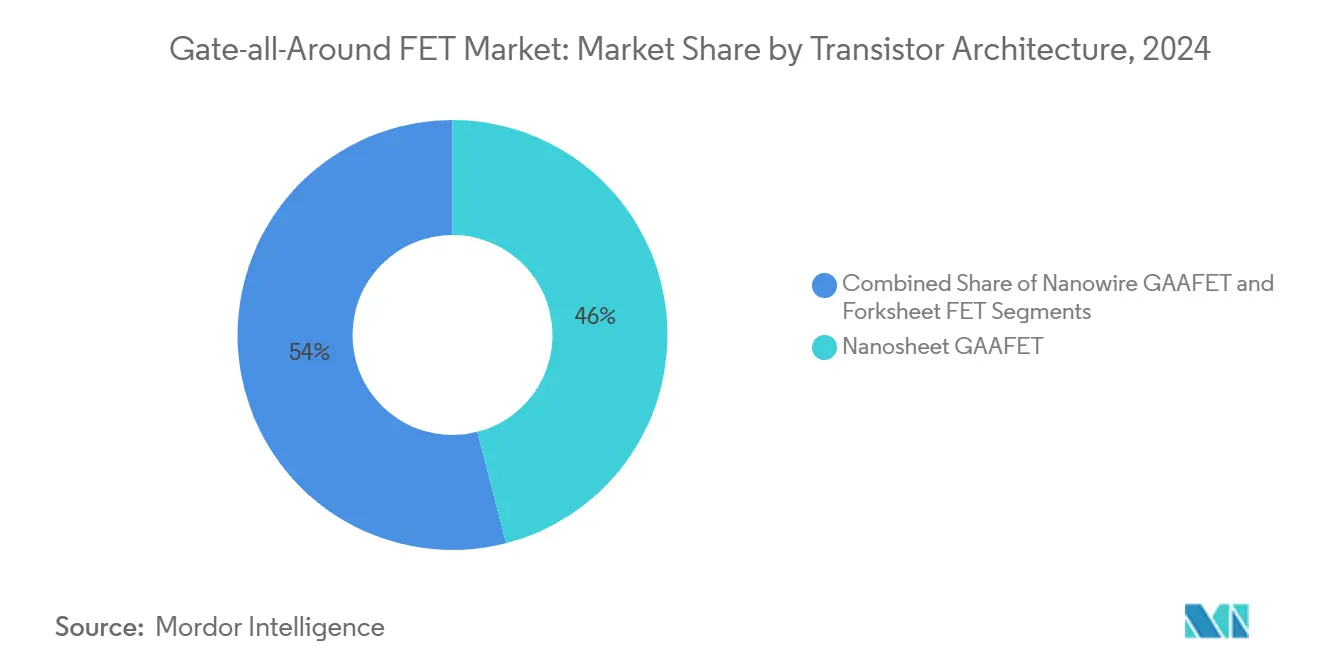
- By transistor architecture, nanosheet designs led with 46% revenue share in 2024 IN the Gate-all-Around FET market; forksheet devices are forecast to expand at an 11.34% CAGR through 2030.
- By wafer size, 300 mm substrates accounted for 63.62% of the Gate-all-Around FET market share in 2024 while recording the highest projected CAGR at 11.78% over the forecast period.
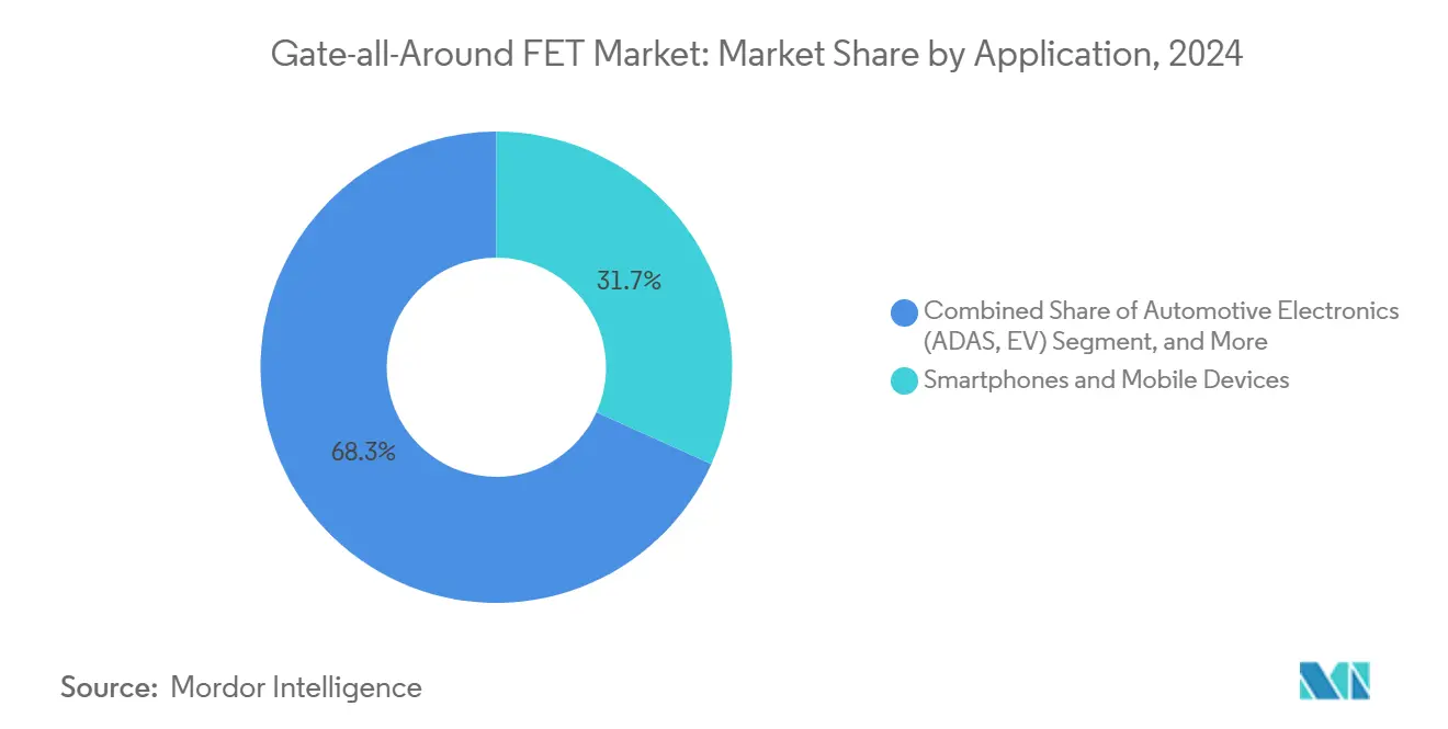
- By application, smartphones and mobile devices held 31.73% of the Gate-all-Around FET market size in 2024, whereas automotive electronics is advancing at a 10.99% CAGR to 2030.
- By end-user, foundries controlled 54.83% of revenue in 2024 of the Gate-all-Around FET market; fabless IC designers present the fastest growth trajectory at an 11.55% CAGR.
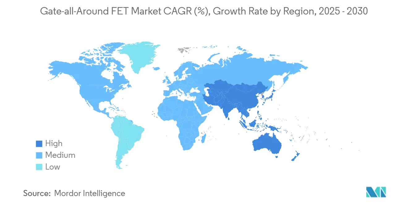
- By geography, Asia-Pacific controlled 56.73% of revenue in 2024 of the Gate-all-Around FET market; Asia-Pacific present the fastest growth trajectory at an 11.66% CAGR.
Global Gate-all-Around FET Market Trends and Insights
Drivers Impact Analysis*
| Driver | (~) % Impact on CAGR Forecast | Geographic Relevance | Impact Timeline |
|---|---|---|---|
| Scaling limits of FinFET below 3 nm | +2.8% | Global with APAC foundry concentration | Medium term (2-4 years) |
| Surging AI and 5G demand for high-performance low-power chips | +2.1% | Global led by North America and APAC | Short term (≤ 2 years) |
| Foundry roadmaps pledging GAAFET production | +1.9% | APAC core and spill-over to North America | Medium term (2-4 years) |
| Backside power-delivery compatibility benefits | +1.4% | Global early adoption in advanced nodes | Long term (≥ 4 years) |
| High-mobility channel material integration | +1.2% | APAC and European research hubs | Long term (≥ 4 years) |
| Advanced-node government incentives | +1.0% | North America, Europe, selective APAC | Medium term (2-4 years) |
| Source: Mordor Intelligence | |||
Scaling limits of FinFET below 3 nm drive architectural transition
FinFETs face fundamental electrostatic limits at channel widths under 5 nm which leads to unacceptable leakage and variability. Gate-all-Around structures restore control by completely enveloping the channel with the gate and therefore sustain Moore’s Law past the 3 nm threshold.[1]L. Kim, “GAAFET Manufacturing Process Optimization,” Journal of Applied Physics, aip.org Leading foundries have invested more than USD 50 billion in Gate-all-Around process development to capture this inevitable transition. Collective R&D accelerates learning cycles that narrow the performance gap between pilot lines and high-volume manufacturing and establishes reliable design rules for ecosystem uptake. The immediate gain in power-performance ratios resonates strongly with mobile and data-center chip designers who compete on performance per watt metrics. These factors elevate Gate-all-Around architectures from a research curiosity to a commercial imperative across advanced nodes.
Surging AI and 5G demand amplifies performance requirements
Artificial intelligence inference engines and 5G radios demand transistors that switch faster at reduced voltages. Vertical gate coverage lowers drain induced barrier lowering and improves sub-threshold slope, permitting operation below 0.7 V without sacrificing speed. Edge AI devices capitalize on such headroom to deliver sustained workloads inside compact thermal envelopes, while 5G macro base stations deploy Gate-all-Around enabled power amplifiers with lower parasitic capacitance for enhanced linearity. GPU vendors validate the performance uplift by taping out next-generation cores exclusively on Gate-all-Around nodes. These high-volume sockets accelerate wafer starts, reduce cost per transistor, and reinforce the technology’s move to mainstream production.
Foundry production roadmaps accelerate commercial deployment
TSMC earmarked USD 40 billion for 2 nm capacity that relies on nanosheet Gate-all-Around devices commencing risk production in 2025. Samsung mirrors this commitment with a comparable nanosheet line aimed at logic and mobile SoCs, while Intel folds Gate-all-Around into a revamped IDM strategy in an effort to regain process parity. Such synchronized roadmaps reassure fabless companies about volume availability and encourage early design engagement. High-volume manufacturing spreads fixed investments across larger output, which consequently drives the cost learning curve down faster than in qualitative pilots. As the fixed overhead is absorbed, accessible price points extend Gate-all-Around uptake to mid-tier product lines beyond flagship phones.
Backside power delivery integration enhances system performance
Gate-all-Around devices pair naturally with backside power-delivery networks that route power beneath the active circuitry, freeing interconnect layers for signal routing and reducing IR drop. Experimental data indicates a 30% improvement in power-delivery efficiency in conjunction with an 8% chip area reduction. These system-level gains resonate most in high-core-count CPUs and GPUs where power integrity directly influences attainable clock frequencies. Early silicon validation by major foundries confirms process co-optimization, bolstering the commercial case for backside power deployment alongside Gate-all-Around logic at 2 nm and below.
Restraints Impact Analysis*
| Restraint | (~) % Impact on CAGR Forecast | Geographic Relevance | Impact Timeline |
|---|---|---|---|
| Immature mass-production yields | -1.8% | Global with highest impact on new entrants | Short term (≤ 2 years) |
| High re-tooling and capital expenditure requirements | -1.2% | Global with concentration in foundry hubs | Medium term (2-4 years) |
| Nascent EDA and IP ecosystem for GAAFET | -0.9% | Global design centers | Short term (≤ 2 years) |
| Self-heating in stacked nanosheets | -0.7% | Global high-performance applications | Medium term (2-4 years) |
| Source: Mordor Intelligence | |||
Manufacturing yield challenges constrain early adoption
Initial Gate-all-Around yield ranges between 40% and 60% versus 85% or higher for mature FinFET lines, raising wafer cost and narrowing commercial viability to premium chips. Yield learning demands statistical process control across multiple epitaxy and etch steps with atomic precision. Variability in nanosheet width or spacing triggers device failure, forcing aggressive binning and price premiums that deter cost-sensitive segments. Early 3 nm runs at a leading Korean foundry reported yields under 50% and prompted selective customer engagement with higher average selling prices. Over the next two years, iterative process refinements and equipment upgrades are expected to raise yields to economic thresholds compatible with high-volume consumer electronics.
Capital expenditure requirements limit industry participation
Gate-all-Around fabrication depends on extreme ultraviolet lithography, atomic layer deposition, selective epitaxy, and high density plasma etch tools that together require near USD 20 billion to outfit a modern 300 mm fab. The capital intensity favors incumbent megafabs and deters smaller IDMs, effectively reshaping competitive dynamics toward a concentrated supplier base. Equipment lead times stretch beyond a year, extending ramp timelines and magnifying execution risk. As a mitigation strategy, select governments underwrite advanced node investments through subsidy programs that offset upfront costs and secure domestic supply lines.
*Our forecasts treat driver/restraint impacts as directional, not additive. The impact forecasts reflect baseline growth, mix effects, and variable interactions.
Segment Analysis
By Transistor Architecture: Nanosheet leadership faces forksheet challenge
Nanosheet devices captured 46% revenue in 2024, underscoring their first-mover edge and alignment with existing FinFET process flows. The Gate-all-Around FET market size for nanosheets is projected to reach USD 54.2 billion by 2030, growing at a 10.1% CAGR as leading foundries standardize this topology in 3 nm and 2 nm offerings. Commercial validation by smartphone flagships and datacenter accelerators accelerates IP reuse and shortens design tape-out cycles. Nanowire derivatives pursue extreme electrostatic control but remain in limited pilot volumes because three-dimensional channel formation multiplies process steps.
Forksheet transistors record an 11.34% CAGR to 2030, the fastest within architecture categories, channeling interest from chip designers that chase density gains beyond nanosheets. Forksheet’s parallel channels and shared diffusions reduce cell height, which directly converts into more cores per die in high-performance use cases. Process maturity lags approximately two years behind nanosheets, yet ecosystem activity rises as early-stage PDKs become available. The technology’s scaling promise positions it to overtake nanosheets late in the decade, provided yield and thermal performance milestones are achieved on schedule.


By Wafer Size: 300 mm dominance reflects manufacturing economics
The 300 mm segment represented 63.62% revenue in 2024 and is forecast to compound at 11.78% annually, outpacing smaller diameters due to lower cost per die and tighter uniformity control. The Gate-all-Around FET market share for 300 mm substrates gains further as all new mega-fabs are specified for this diameter. High equipment utilization rates and larger die yields create a resilient cost structure that appeals to both foundry and fabless business models. Continuous improvements in substrate defect density and equipment throughput reinforce the economic advantage of staying on 300 mm for at least the next two process nodes.
Sub-300 mm wafers persist mainly in R&D and low-volume specialty logic where legacy tool sets prevail. Conversion economics do not justify retrofitting older 200 mm lines with EUV capability, so these nodes confine themselves to power devices, sensors, and specialty analog that do not require atomic-scale gates. Below 150 mm, academic and pilot facilities rely on the smaller platform for flexibility and rapid changes in experimental wafer runs. While incremental niche revenues remain, migration to 300 mm in volume logic production is effectively complete.
By Application: Mobile dominance yields to automotive growth
Smartphones and mobile devices commanded 31.73% revenue in 2024, sustaining the first commercial deployments of Gate-all-Around logic in 3 nm application processors. Tier-one handset OEMs prioritize power efficiency and battery life, parameters that directly benefit from the lower subthreshold slope of the new architecture. As mobile penetration matures, share gains slow, yet unit scale remains attractive for capacity fills.
Automotive electronics posts a brisk 10.99% CAGR through 2030, fueled by advanced driver assistance systems, zonal controllers, and powertrain inverters that require dense compute with strict thermal profiles. Functional safety mandates heighten the need for predictable electrical behavior over extended temperature ranges, attributes enabled by Gate-all-Around transistors’ superior gate control. Lengthy qualification cycles mean revenue ramps lag mobile introductions, but once validated, automotive demand sustains multi-year volume certainty that stabilizes fab utilization.
By End-User Industry: Foundries lead while fabless designers accelerate
Foundries generated 54.83% of 2024 sales, reflecting their pivotal role in manufacturing and technology enablement. The Gate-all-Around FET market is expected to see foundry revenue advance steadily as more design houses migrate advanced nodes to external manufacturing partners. Capacity allocation policies favor strategic commitments and yield learning partnerships that lower per-die cost over time.
Fabless IC designers, growing at 11.55% per year, leverage the foundry model to gain early access to 2 nm and forksheet nodes without capital outlays. Rapid iteration in AI accelerators, networking ASICs, and custom compute silicon positions these firms to monetize the performance-per-watt upside swiftly. Integrated device manufacturers weigh the balance between investing in captive Gate-all-Around capacity and tapping external foundries, a decision that hinges on volume forecasts, funding access, and strategic control considerations.
Geography Analysis
Asia-Pacific carried 56.73% share in 2024 and is projected to expand at 11.66% CAGR to 2030, propelled by Taiwan’s dominant foundry footprint, South Korea’s process breakthroughs, and substantial Chinese state funding. Regional governments subsidize advanced equipment purchases, swift utility hook-ups, and workforce development to anchor fabrication onshore. Local clustering of design, packaging, and test services forms end-to-end ecosystems that shorten cycle times and lower logistical overhead. High density of smartphone OEMs and HPC designers ensures stable demand queues that fill 2 nm and 3 nm lines as soon as capacity opens.
North America commands sizeable revenue anchored in a vibrant fabless hub and renewed federal incentives under the CHIPS and Science Act, which earmarks USD 52 billion for domestic manufacturing.[2]U.S. Department of Commerce, “CHIPS Act Implementation Update,” commerce.gov Intel’s multibillion investments in Arizona and Ohio target 2 nm Gate-all-Around volumes, aiming to blend internal usage with foundry services for external customers. Proximity between design centers in California, Texas, and Massachusetts and pilot fabs tightens feedback loops that speed device optimization.
Europe pursues technology sovereignty by funding pilot lines and ecosystem build-outs through the European Chips Act.[3]European Commission, “European Chips Act Implementation,” europa.eu Germany’s automotive supply chain pushes for long-term local access to Gate-all-Around chips that meet functional safety protocols. The Netherlands’ ASML remains central to lithography enablement, while new initiatives in France and Italy foster design IP and packaging capabilities. Although the region trails APAC in capacity, its specialized automotive and industrial focus delivers a stable demand mix with higher margins. The Middle East and Africa currently serve as an emerging demand pool for consumer electronics and data centers but lack meaningful fabrication. Investments in knowledge transfer and training programs are underway to create initial design hubs that can eventually anchor small-scale manufacturing.

Competitive Landscape
Gate-all-Around FET market competition centers on a small cadre of players that control leading edge process nodes and have the balance sheet to deploy multibillion-dollar capex. TSMC, Samsung, and Intel own the majority of active 2 nm roadmaps, creating a tri-lateral race to secure early customer tape-out commitments. Each firm invests aggressively in yield ramp programs, materials innovation, and equipment partnerships to shorten time to cost parity with mature FinFET nodes. Equipment suppliers such as ASML, Applied Materials, and Lam Research engage in joint development projects that align tool roadmaps with foundry production timelines. Strategic supplier–customer interlocks protect process know-how and mitigate supply chain risk.
Intellectual property depth and aligned EDA tool flows form secondary competitive fronts. Cadence and Synopsys release Gate-all-Around optimized libraries and design rule kits that shave months from layout cycles, increasing stickiness with early adopter designers. Patent filings on selective epi, backside power routing, and low-k spacer materials escalate, prompting broader cross-licensing arrangements that keep litigation exposure manageable.[4]United States Patent and Trademark Office, “Patent Database Search Results,” uspto.gov Barriers to entry rise as each incumbent secures ecosystem lock-in across capital equipment, process recipes, and IP availability. Nevertheless, niche opportunities persist for specialist foundries and research fabs serving automotive, aerospace, or defense programs that value tailored reliability features over pure cost.
Looking ahead, competition may pivot toward forksheet and complementary stacked nanosheet topologies as density and performance ceilings approach for standard nanosheets. Early R&D consortia aim to define patterning schemes and align precursor chemistries slotting into existing 300 mm lines. If yields track the nanosheet learning curve, time-to-profit windows could compress, raising pressure on lagging players to either license, partner, or exit advanced logic altogether. Vendors that can master both front-end device scaling and back-end power delivery integration stand to secure above market returns throughout the forecast horizon.
Gate-all-Around FET Industry Leaders
Taiwan Semiconductor Manufacturing Company Limited
Samsung Electronics Co., Ltd.
Intel Corporation
GlobalFoundries Inc.
Semiconductor Manufacturing International Corporation
- *Disclaimer: Major Players sorted in no particular order

Recent Industry Developments
- March 2025: TSMC expanded 2 nm Gate-all-Around capacity in Taiwan with a USD 12 billion investment to support high-volume manufacturing planned for 2026.
- February 2025: Samsung won USD 8.5 billion in Korean incentives earmarked for Gate-all-Around scaling and yield optimization programs.
- January 2025: Intel acquired advanced packaging technology from a European equipment firm for USD 2.3 billion to accelerate Gate-all-Around integration in HPC processors.
- December 2024: Applied Materials unveiled selective deposition systems tailored for nanosheet channel formation, addressing a key yield limiter.


Global Gate-all-Around FET Market Report Scope
| Nanosheet GAAFET |
| Nanowire GAAFET |
| Forksheet FET |
| 300 mm |
| 200 mm |
| Below 150 mm |
| Smartphones and Mobile Devices |
| High-Performance Computing and Data Centers |
| Automotive Electronics (ADAS, EV) |
| Internet of Things and Edge Devices |
| RF and Analog |
| Other Applications |
| Foundries |
| Integrated Device Manufacturers (IDMs) |
| Fabless IC Designers |
| Research and Academia |
| North America | United States |
| Canada | |
| Mexico | |
| South America | Brazil |
| Rest of South America | |
| Europe | Germany |
| France | |
| United Kingdom | |
| Rest of Europe | |
| Asia-Pacific | China |
| Taiwan | |
| South Korea | |
| Japan | |
| India | |
| Rest of Asia-Pacific | |
| Middle East and Africa | Middle East |
| Africa |
| By Transistor Architecture | Nanosheet GAAFET | |
| Nanowire GAAFET | ||
| Forksheet FET | ||
| By Wafer Size | 300 mm | |
| 200 mm | ||
| Below 150 mm | ||
| By Application | Smartphones and Mobile Devices | |
| High-Performance Computing and Data Centers | ||
| Automotive Electronics (ADAS, EV) | ||
| Internet of Things and Edge Devices | ||
| RF and Analog | ||
| Other Applications | ||
| By End-User Industry | Foundries | |
| Integrated Device Manufacturers (IDMs) | ||
| Fabless IC Designers | ||
| Research and Academia | ||
| By Geography | North America | United States |
| Canada | ||
| Mexico | ||
| South America | Brazil | |
| Rest of South America | ||
| Europe | Germany | |
| France | ||
| United Kingdom | ||
| Rest of Europe | ||
| Asia-Pacific | China | |
| Taiwan | ||
| South Korea | ||
| Japan | ||
| India | ||
| Rest of Asia-Pacific | ||
| Middle East and Africa | Middle East | |
| Africa | ||


Key Questions Answered in the Report
What is the projected revenue for Gate-all-Around FET (GAAFET)devices by 2030?
The segment is forecast to reach USD 117.86 billion by 2030 on a 10.40% CAGR.
Which region leads in advanced Gate-all-Around fabrication capacity?
Asia-Pacific holds 56.73% revenue in 2024 due to strong Taiwanese and Korean foundry footprints.
Why are nanosheet transistors dominant today?
They align with existing FinFET process flows, enabling faster yield ramps and cost efficiencies that secured 46% of 2024 sales.
How fast will forksheet technology grow?
Forksheet devices are expected to expand at 11.34% CAGR through 2030 driven by higher transistor density.
What drives Gate-all-Around adoption in automotive electronics?
ADAS and electric drive systems require power-efficient high-compute chips, propelling a 10.99% CAGR in automotive uptake.
Page last updated on:


