Diffractive Optical Elements Market Size and Share
Market Overview
| Study Period | 2021 - 2031 |
|---|---|
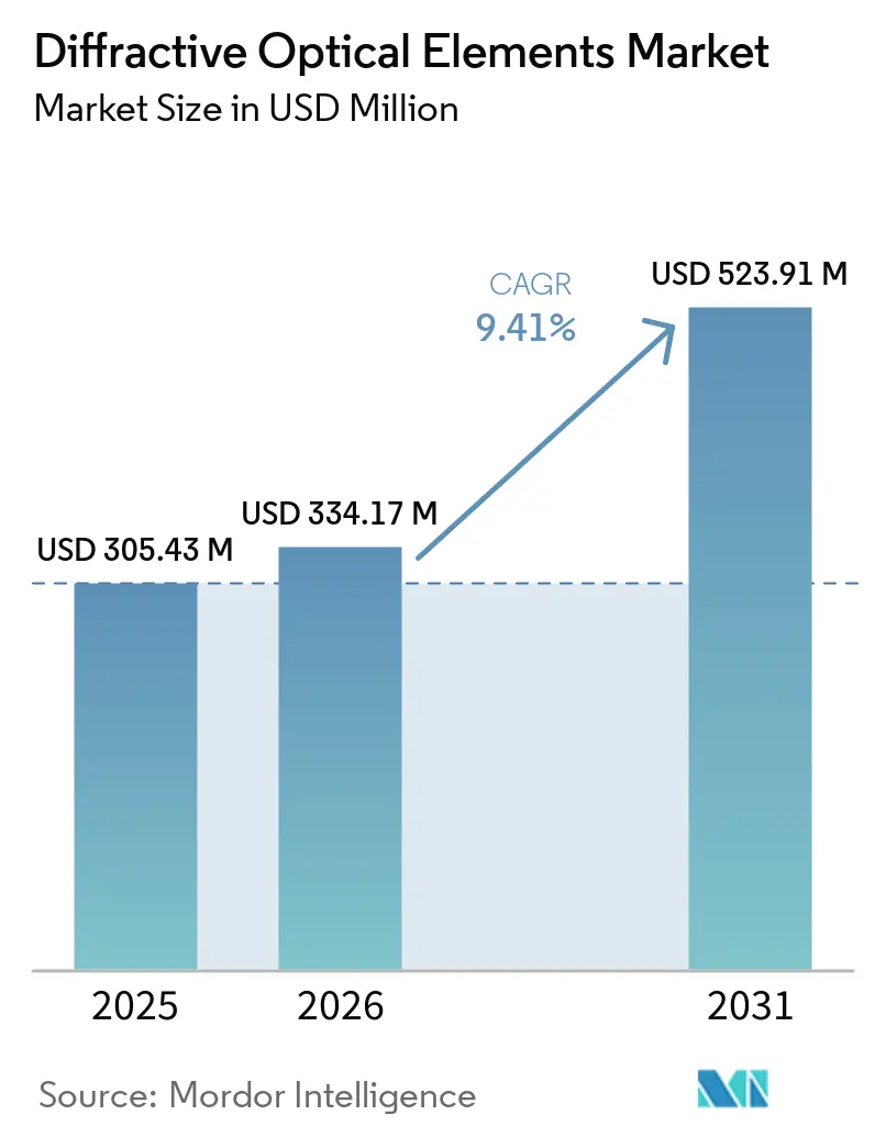
| Market Size (2026) | USD 334.17 Million |
| Market Size (2031) | USD 523.91 Million |
| Growth Rate (2026 - 2031) | 9.41% CAGR |
| Fastest Growing Market | Asia Pacific |
| Largest Market | Asia Pacific |
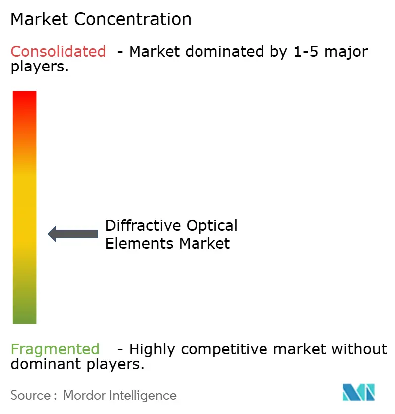
| Market Concentration | Medium |
Major Players *Disclaimer: Major Players sorted in no particular order Image © Mordor Intelligence. Reuse requires attribution under CC BY 4.0. | |
Diffractive Optical Elements Market Analysis by Mordor Intelligence
The diffractive optical elements market was USD 305.43 million in 2025 and USD 334.17 million in 2026, and is forecast to reach USD 523.91 million by 2031, growing at a CAGR of 9.41% from 2026 to 2031. Widening use in laser material processing, smartphone 3-D sensing, and automotive LiDAR is driving demand for wafer-scale beam-shaping solutions that can withstand kilowatt-class power while shrinking module height to below 20 millimeters. Polymer and silicon-nitride metasurfaces are moving into high-volume consumer products as cost pressures favor injection-molded replication over photolithography-etched fused silica. Defense programs continue to specify diamond or fused-silica substrates for extreme thermal conductivity and laser-induced damage thresholds above 10 J/cm². With Asia-Pacific fabs ramping roll-to-roll metalens printing and North American data-center operators investing in silicon photonics, the competitive field now spans legacy optics houses, fab-lite metasurface startups, and vertically integrated semiconductor suppliers.
Key Report Takeaways
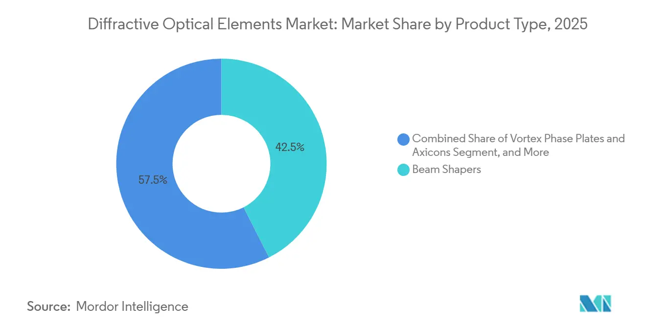
- By product type, beam shapers led with 42.52% of 2025 revenue, whereas vortex phase plates and axicons are advancing at an 11.42% CAGR through 2031.
- By material, fused silica and quartz captured 51.85% of 2025 sales, while diamond substrates recorded the fastest expansion at a 12.21% CAGR in 2031.
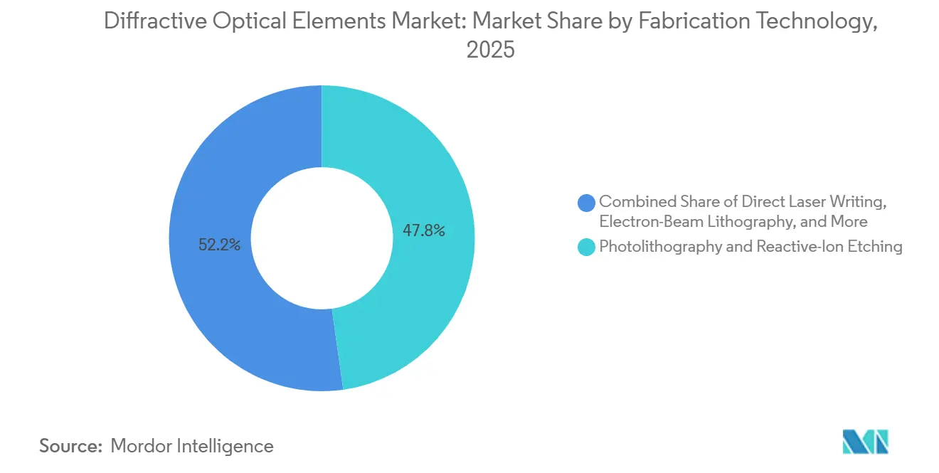
- By fabrication technology, photolithography-reactive ion etching accounted for 47.78% of 2025 revenue, whereas nano-imprint and injection molding are rising at a 10.56% CAGR to 2031.
- By application, laser material processing claimed 37.23% of 2025 revenue, while augmented and virtual reality displays are forecast to grow at a 13.24% CAGR in 2031.
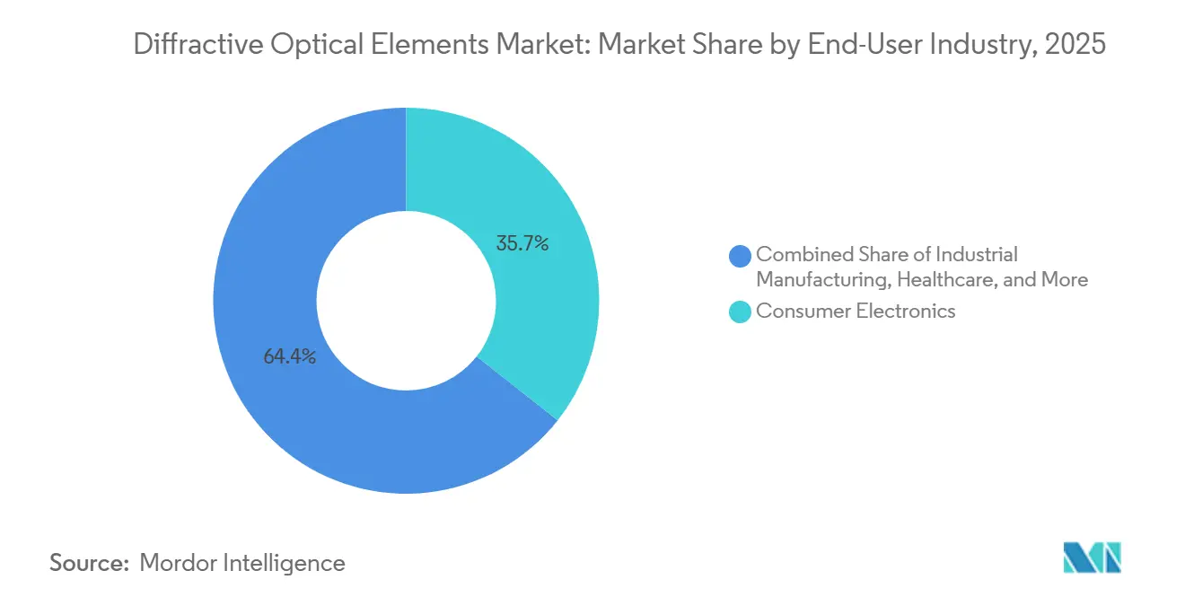
- By end-user industry, consumer electronics generated 35.65% of 2025 revenue, yet healthcare is projected to expand at a 12.65% CAGR in 2031.
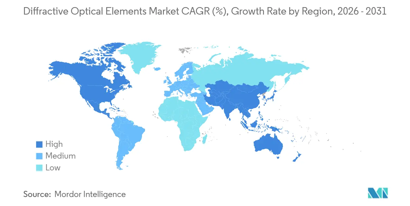
- By geography, Asia-Pacific accounted for 40.32% of 2025 revenue and is projected to grow at a 12.89% CAGR through 2031.
Note: Market size and forecast figures in this report are generated using Mordor Intelligence’s proprietary estimation framework, updated with the latest available data and insights as of January 2026.
Global Diffractive Optical Elements Market Trends and Insights
Drivers Impact Analysis*
| Driver | (~) % Impact on CAGR Forecast | Geographic Relevance | Impact Timeline |
|---|---|---|---|
| Rising Adoption of Beam-Shaping DOEs in High-Power Fiber Lasers | +2.1% | Germany, China, Japan | Medium term (2-4 years) |
| Cost Reduction Pressure Accelerating Injection-Molded Polymer DOEs | +1.8% | Asia-Pacific core, North America spill-over | Short term (≤ 2 years) |
| Surge in Automotive LiDAR Programs Integrating Meta-Surface DOEs | +1.6% | North America and Europe OEMs, Asia-Pacific manufacturing | Medium term (2-4 years) |
| Emerging Quantum Photonics Applications Requiring Complex Phase Plates | +0.9% | North America research labs, European consortia | Long term (≥ 4 years) |
| Increased Deployment of 3-D Sensing Cameras in Smartphones | +1.4% | China, South Korea, Japan, United States | Short term (≤ 2 years) |
| Defense Investments in High-Energy Laser Weapon Beam Splitters | +1.3% | United States, Middle East allies | Medium term (2-4 years) |
| Source: Mordor Intelligence | |||
Rising Adoption Of Beam-Shaping DOEs In High-Power Fiber Lasers
In the diffractive optical elements market, industrial welding, cutting, and additive manufacturing require uniform irradiance profiles that refractive optics cannot maintain at multi-kilowatt power levels. Recent nanoimprint-fabricated elements combine beam shaping and splitting in a single wafer, cutting part count and thermal lensing risks. Thin fused-silica substrates maintain high damage thresholds and minimal dispersion for femtosecond pulses, while off-the-shelf availability has trimmed traditional 8-12 week lead times to a matter of days, accelerating system-integrator deployment.[1]Coherent Corp., “Diffractive Optical Elements for High-Power Industrial Lasers,” coherent.comIndustrial laser lines for battery welding, sheet cutting, and turbine drilling require uniform irradiance that conventional refractive optics cannot deliver at kilowatt levels, so integrators now specify fused-silica diffractive beam shapers that withstand >10 J cm⁻² fluence with negligible dispersion.
Cost Reduction Pressure Accelerating Injection-Molded Polymer DOEs
Injection molding and nanoimprint replication reduce unit cost by roughly one order of magnitude versus etched fused silica. In 2026, a smartphone platform integrated nanopillar metasurfaces, achieving a 73% cost reduction and paving the way for mass-market 3-D sensing.[2]arXiv Authors, “iPhone 17 Pro Max Metasurface DOE Integration,” arxiv.org Metalenz licensed its metasurface IP to STMicroelectronics, and more than 140 million polymer metasurface units shipped by mid-2025, confirming the yield scalability of wafer-level replication. VIAOPTIC studies show that polymethyl methacrylate delivers high optical purity, while polycarbonate withstands 145 °C cabin peaks, so handset and automotive Tier-1s match polymers to use cases.
Surge in Automotive LiDAR Programs Integrating Meta-Surface DOEs
Level 2+ advanced driver assistance systems demand wide-field-of-view beam steering without bulky scanning mirrors in the diffractive optical elements market. Single-layer metasurface objectives demonstrated in 2026 offer sub-10-minute grayscale-lithography cycle times and material costs near USD 23 per micrometer of phase depth.[3]American Chemical Society, “Low-Cost Grayscale Lithography for DOEs,” acs.orgPartnerships between optic suppliers and perception-software firms are pushing integration into 2027 model-year vehicles, with micro-lens arrays reducing module height for flush roofline installation. Automotive original equipment manufacturers seek solid-state LiDAR that fits rooflines under 20 mm tall, and metasurface beam splitters remove bulky refractive expanders while steering multiple dots across a 120-degree horizontal field.
Increased Deployment Of Three-Dimensional Sensing Cameras In Smartphones
Quantum computing and secure communications require orbital-angular-momentum beams and entangled-photon sources, which static diffractive elements provide more efficiently than spatial light modulators. Vortex phase plates have generated optical skyrmion lattices with topological stability, while monolithic phase-modulated laser arrays shrink quantum sensor footprints tenfold.[4]American Physical Society, “Optical Skyrmion Lattices Using Q-Plates,” aps.orgStructured-light depth cameras rely on uniform speckle projection, and metasurface DOEs now integrate directly atop vertical-cavity surface-emitting lasers, creating a single packaged emitter less than 1 mm thick. STMicroelectronics hit its 140 million-unit milestone by embedding Metalenz metasurfaces inside standard time-of-flight packages, proving that CMOS fabs can handle diffractive top layers without downstream bottlenecks.
Restraints Impact Analysis*
| Restraint | (~) % Impact on CAGR Forecast | Geographic Relevance | Impact Timeline |
|---|---|---|---|
| High Precision Fabrication Cost for Sub-Micron Features | -1.4% | North America and Europe high-mix lines | Short term (≤ 2 years) |
| Limited Thermal Stability of Polymer DOEs in Harsh Environments | -0.8% | Middle East and Africa outdoor sensors, global automotive | Medium term (2-4 years) |
| Supply Chain Bottlenecks for Ultrapure Fused Silica Blanks | -0.6% | Global semiconductor lithography and defense programs | Medium term (2-4 years) |
| IP Fragmentation Hindering Standardization Across Suppliers | -0.5% | Global AR/VR and EUV ecosystems | Long term (≥ 4 years) |
| Source: Mordor Intelligence | |||
High Precision Fabrication Cost for Sub-Micron Features
In the diffractive optical elements market, photolithography combined with reactive-ion etching delivers ±5-nanometer depth control, yet throughput remains near 15 cm² per hour on 150-millimeter wafers, pushing custom DOE prices above USD 500 per piece. Grayscale-lithography shortcuts can lower cost but are limited to binary or four-level phase structures, which restricts advanced wavefront engineering. The resulting bifurcation places nanoimprint lines in consumer electronics and direct-write shops in aerospace, leaving mid-volume tooling underserved.
Limited Thermal Stability of Polymer DOEs in Harsh Environments
PMMA gratings lost 12% reflectivity when heated from 20 °C to 80 °C in fiber tests, which disqualifies bare polymer optics for Middle Eastern roadside LiDAR and under-hood cameras. Polycarbonate withstands 145 °C peaks but introduces chromatic blur due to a lower Abbe number, so automotive Tier-1s either accept color fringes or revert to glass. CYTOP fluoropolymer retains efficiency across the same span but costs more and remains hard to pattern on circular fibers. Adhesively bonding thin polymer DOEs to fused silica mitigates heat, but differential thermal expansion can delaminate layers during prolonged desert cycles. These reliability risks cap polymer share in harsh-environment deployments.
*Our forecasts treat driver/restraint impacts as directional, not additive. The impact forecasts reflect baseline growth, mix effects, and variable interactions.
Segment Analysis
By Product Type: Beam Shapers Dominate While Vortex Plates Gain Momentum
Beam shapers captured 42.52% of 2025 revenue, reflecting their role in battery-pack welding, turbine-blade drilling, and sheet-metal cutting lines where top-hat profiles prevent edge burn-through. Diffractive diffusers also support fractional dermatology lasers cleared by the U.S. FDA, enabling uniform micro-spot arrays that quicken patient recovery. The diffractive optical elements market for beam shapers is expected to continue expanding as industrial OEMs prequalify off-the-shelf diffusers to shorten design cycles.
Vortex phase plates and axicons are projected to grow at an 11.42% CAGR through 2031, as quantum research teams exploit orbital-angular-momentum beams for information encoding. Demonstrations of spiral zone plates with 40% first-order efficiency point toward optical trapping and free-space communication payloads. Although unit volumes remain modest, the diffractive optical elements market share held by vortex products is poised to expand as chip-scale phase-modulated lasers enter commercial quantum sensors.


By Material: Fused-Silica Leads While Diamond Substrates Emerge
Fused-silica and quartz supplied 51.85% of 2025 material revenue thanks to low thermal expansion below 0.5 ppm/K and UV-to-IR transmission that meets semiconductor lithography and high-energy laser demands. Global capacity, however, is constrained by parts-per-billion impurity specifications that only a handful of suppliers achieve, prolonging lead times for next-generation EUV optics. The diffractive optical elements market size tied to fused-silica products, therefore, commands a pricing premium that buffers suppliers against commodity pressures.
Diamond substrates are forecast to clock a 12.21% CAGR on the back of defense laser splitters requiring thermal conductivity near 2000 W/m-K. SBIR awards in the United States have enabled small-batch production of 300-kilowatt continuous-wave systems, validating technical feasibility even as wafer costs exceed USD 5,000 per 100-millimeter wafer. Once deposition yields improve, diamond could erode fused silica’s market share in diffractive optical elements for weapon-class applications.
By Fabrication Technology: Photolithography-RIE Remains Predominant, Nano-Imprint Surges
Photolithography with reactive-ion etching accounted for 47.78% of 2025 revenue by delivering sub-100-nanometer features and depth control within ±5 nanometers, benchmarks still unmatched at an increased throughput of 15 cm² per hour on a 150-millimeter mass scale. Hybrid femtosecond-laser plus ICP-RIE flows have increased throughput to 15 cm² per hour on 150-millimeter wafers, keeping the platform relevant for semiconductor-grade DOEs.
Nano-imprint and injection-molded lines are projected to post a 10.56% CAGR through 2031 as consumer electronics aim to bring unit costs below USD 1. Roll-to-roll metalens printing in South Korea surpassed 300 lenses per second at>90% efficiency in 2026, demonstrating the volume potential. If defect density can be tamed, these routes may capture a larger slice of the diffractive optical elements market size for smartphone and AR glasses optics.
By Application: Laser Processing Anchors, AR/VR Displays Accelerate
Laser material processing accounted for 37.23% of 2025 revenue, driven by automotive and renewable energy manufacturing lines. DOE beam splitters that multiply beams onto photovoltaic wafers boost throughput past 0.19 m²/min, supporting gigawatt-scale cell plants. Healthcare lasers rely on diffractive homogenizers to minimize hot spots, enhancing patient comfort during dermatology procedures cleared under recent FDA 510(k) filings.
AR/VR and holographic displays are expected to expand at a 13.24% CAGR through 2031 as thin waveguide combiners replace bulky refractive stacks. A 2024 Nature study demonstrated full-color holographic optics with sub-millimeter thickness, signaling readiness for consumer headsets. This upswing should broaden the footprint of the diffractive optical elements industry in entertainment and enterprise training.
By End-User Industry: Consumer Electronics Leads, Healthcare Grows Fastest
Smartphones, tablets, and wearables held 35.65% of 2025 revenue, embedding metasurface diffusers for facial recognition and depth mapping. Shipment volumes above 140 million units validate the cost model of wafer-level replication at ≥200 millimeter diameters. Industrial manufacturers rely on DOE beam shapers to raise yields in battery welding and turbine drilling, while aerospace firms adopt reflective DOEs that eliminate chromatic dispersion in ultrafast machining.
Healthcare is forecast to record a 12.65% CAGR as multifocal intraocular lenses and fractional dermatology systems exploit diffractive zones to deliver simultaneous near and distance vision. As presbyopia incidence climbs with aging populations, the diffractive optical elements market size in ophthalmology devices is set to widen, aided by continual FDA approvals that assure clinic adoption.
Geography Analysis
Asia-Pacific generated 40.32% of 2025 revenue and is on track for a 12.89% CAGR through 2031. Wafer-scale metasurface projects in Tianjin and roll-to-roll metalens printing breakthroughs in South Korea point to dominant regional capacity, while Japanese optoelectronics firms commercialize phase-modulated laser arrays that collapse module footprints. Local governments continue to subsidize 12-inch wafer fabs that will push the diffractive optical elements market deeper into consumer electronics and automotive perception modules.
North America benefits from defense funding and the expansion of cloud data centers. A USD 2 billion equity investment tied to AI optical interconnects underscores a strategic commitment to wafer-level DOE fabrication. Concurrent SBIR awards target 300-kilowatt naval laser splitters, aligning with diamond-substrate development timelines. The region, therefore, balances high-mix aerospace orders with volume silicon photonics programs, diversifying its share of the diffractive optical elements market.
Europe sustains momentum through automotive LiDAR integration and semiconductor lithography optics. Clean-room expansions in Germany will add EUV and high-NA immersion capacity by 2027, while regional carmakers specify metasurface beam shapers to meet Euro NCAP safety targets. South America, the Middle East and Africa remain nascent, but solar-panel texturing and oil-field inspection create niche demand for rugged fused-silica DOEs in high-temperature and high-dust conditions.

Competitive Landscape
Competition is moderately fragmented. Legacy vendors such as Jenoptik and Coherent integrate design, lithography, and metrology under one roof, commanding loyalty from industrial laser integrators. Specialized DOE producers, including HOLO/OR and SILIOS, win on depth-of-expertise, supplying custom phase profiles with damage thresholds above 10 J/cm². Metasurface startups led by Metalenz and Meta Materials leverage nanoimprint replication to undercut etched fused-silica pricing by up to 70%, shifting bargaining power in consumer electronics.
Several firms pursue vertical integration: Coherent’s eight-week rapid-prototype service spans nanoimprint, lithography, and glass molding, while Edmund Optics’ acquisition of an ultra-precision machining firm adds diamond-turning capability for hybrid refractive-diffractive optics. Patent portfolios around EUV zone plates and AR waveguides remain concentrated, yet ISO 15902:2019 vocabulary adoption eases multi-supplier qualification, enabling OEMs to dual-source without redesigning fixture libraries.
Technology differentiation centers on laser-induced damage resistance, chromatic dispersion management, and thermal stability. Reflective coatings on fused-silica DOEs eliminate dispersion for sub-200-fs pulses, whereas CYTOP-based polymer gratings maintain efficiency across 20 °C-80 °C. Diamond-substrate development, though capital intensive, promises unmatched heat dissipation for future 500 kilowatt directed-energy platforms. With cost and performance vectors now diverging between consumer and defense markets, supplier positioning hinges on mastering both wafer-level replication and ultra-high-precision etching.
Diffractive Optical Elements Industry Leaders
Carl Zeiss AG
Jenoptik AG
HOLO/OR Ltd.
SUSS MicroTec SE
Coherent Corp.
- *Disclaimer: Major Players sorted in no particular order

Recent Industry Developments
- April 2026: Apple integrated nanopillar metasurface DOEs into the iPhone 17 Pro Max Face ID module, realizing a 73% cost drop versus fused-silica diffusers.
- April 2026: South Korean researchers demonstrated roll-to-roll metalens printing at 300 lenses per second and 90% efficiency, signaling high-volume readiness.
- April 2026: Kunyou Optoelectronics secured CNY 400 million (USD 55 million) Series C+ for wafer-level optics aimed at smartphone camera modules.
- March 2026: NVIDIA invested USD 2 billion in Coherent to expand silicon photonics and optical interconnect capacity for AI data centers.


Global Diffractive Optical Elements Market Report Scope
Diffractive Optical Elements (DOE) are optical components that use micro- or nano-structured surface patterns to manipulate light through diffraction, enabling functions such as beam shaping, beam splitting, diffusion, and phase modulation by precisely controlling the wavefront of incident light.
The Diffractive Optical Elements Market Report is Segmented by Product Type (Beam Shapers, Diffusers, Beam Splitters, Vortex Plates), Material (Fused Silica, Polymers, Silicon, Diamond), Fabrication (Photolithography-RIE, Laser Writing, E-Beam, Nano-Imprint), Application (Laser Processing, Medical, 3D Sensing, Optical Comms, AR/VR), End-User (Industrial, Healthcare, Consumer Electronics, Automotive, Aerospace), and Geography (North America, South America, Europe, Asia-Pacific, Middle East and Africa). The Market Forecasts are Provided in Terms of Value (USD).
| Beam Shapers |
| Diffusers/Homogenizers |
| Beam Splitters |
| Vortex Phase Plates and Axicons |
| Fused Silica and Quartz |
| Polymers (PMMA, Polycarbonate, Zeonex) |
| Silicon and Silicon Nitride |
| Diamond |
| Photolithography and Reactive-Ion Etching |
| Direct Laser Writing |
| Electron-Beam Lithography |
| Nano-Imprint / Injection Molding |
| Laser Material Processing |
| Medical and Aesthetic Procedures |
| 3-D Sensing and LiDAR |
| Optical Communications and Free-Space Optics |
| AR/VR and Holographic Displays |
| Industrial Manufacturing |
| Healthcare |
| Consumer Electronics |
| Automotive and Transportation |
| Aerospace and Defense |
| North America | United States |
| Canada | |
| Mexico | |
| South America | Brazil |
| Argentina | |
| Rest of South America | |
| Europe | Germany |
| France | |
| United Kingdom | |
| Italy | |
| Rest of Europe | |
| Asia-Pacific | China |
| Japan | |
| South Korea | |
| India | |
| Rest of Asia-Pacific | |
| Middle East and Africa |
| By Product Type | Beam Shapers | |
| Diffusers/Homogenizers | ||
| Beam Splitters | ||
| Vortex Phase Plates and Axicons | ||
| By Material | Fused Silica and Quartz | |
| Polymers (PMMA, Polycarbonate, Zeonex) | ||
| Silicon and Silicon Nitride | ||
| Diamond | ||
| By Fabrication Technology | Photolithography and Reactive-Ion Etching | |
| Direct Laser Writing | ||
| Electron-Beam Lithography | ||
| Nano-Imprint / Injection Molding | ||
| By Application | Laser Material Processing | |
| Medical and Aesthetic Procedures | ||
| 3-D Sensing and LiDAR | ||
| Optical Communications and Free-Space Optics | ||
| AR/VR and Holographic Displays | ||
| By End-User Industry | Industrial Manufacturing | |
| Healthcare | ||
| Consumer Electronics | ||
| Automotive and Transportation | ||
| Aerospace and Defense | ||
| By Geography | North America | United States |
| Canada | ||
| Mexico | ||
| South America | Brazil | |
| Argentina | ||
| Rest of South America | ||
| Europe | Germany | |
| France | ||
| United Kingdom | ||
| Italy | ||
| Rest of Europe | ||
| Asia-Pacific | China | |
| Japan | ||
| South Korea | ||
| India | ||
| Rest of Asia-Pacific | ||
| Middle East and Africa | ||


Key Questions Answered in the Report
What is the current diffractive optical elements market size and how fast is it growing?
The diffractive optical elements market size stands at USD 334.17 million in 2026 and is forecast to reach USD 523.91 million by 2031, advancing at a 9.41% CAGR, according to Mordor Intelligence.
Which region leads demand for diffractive optical elements?
Asia-Pacific accounts for 40.32% of 2025 revenue and is forecast to remain the largest as wafer-scale metasurface capacity comes online in China and South Korea.
Which product segment is growing the fastest?
Vortex phase plates and axicons are expected to register an 11.42% CAGR through 2031, driven by quantum photonics and atmospheric research programs.
Why are diamond substrates gaining interest?
Defense laser systems need extreme thermal conductivity and radiation hardness, properties that chemical-vapor-deposited diamond provides, supporting a projected 12.21% CAGR for diamond-based DOEs.
How are cost pressures being addressed in consumer applications?
Injection-molded metasurface optics cut unit prices by up to 70% versus etched fused-silica, enabling high-volume smartphone and AR headset deployment.
What restraint could most slow market growth?
High-precision sub-micron fabrication remains expensive, with custom etched DOEs still exceeding USD 500 per piece, tempering adoption in price-sensitive segments.
Page last updated on:


