Diffractive Optical Element Market Size and Share
Market Overview
| Study Period | 2019 - 2030 |
|---|---|
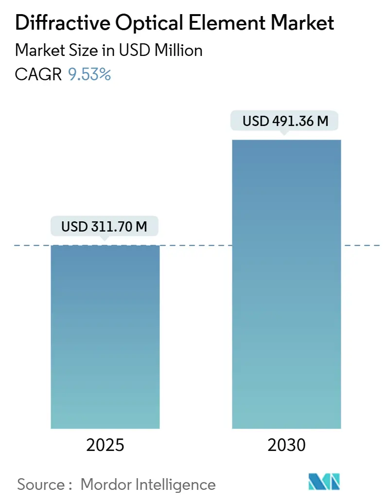
| Market Size (2025) | USD 311.70 Million |
| Market Size (2030) | USD 491.36 Million |
| Growth Rate (2025 - 2030) | 9.53% CAGR |
| Fastest Growing Market | Asia Pacific |
| Largest Market | Asia Pacific |
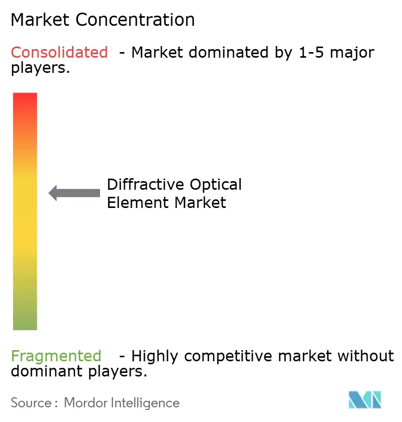
| Market Concentration | Medium |
Major Players *Disclaimer: Major Players sorted in no particular order Image © Mordor Intelligence. Reuse requires attribution under CC BY 4.0. | |
Diffractive Optical Element Market Analysis by Mordor Intelligence
The diffractive optical element market size reached USD 311.70 million in 2025 and is forecast to attain USD 491.36 million by 2030, translating to a 9.53% CAGR. Market expansion is fueled by extreme ultraviolet lithography investments, growing automotive LiDAR deployments, and structured-light 3D sensing in flagship smartphones. Precision metasurface designs improve energy efficiency in high-power laser processing, while standardized libraries in silicon photonics reduce development costs for telecom transceivers. Supply chain localization policies in China and the United States channel capital toward domestic foundries, tightening lead-times for large-area fused-silica parts. Vendor focus on metasurface production processes improves wafer-level yields and lowers per-unit costs for consumer electronics assemblies.
Key Report Takeaways
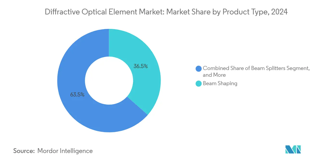
- By product type, beam shaping elements held 36.52% of the diffractive optical element market share in 2024. Vortex phase plates are projected to expand at a 10.13% CAGR through 2030.
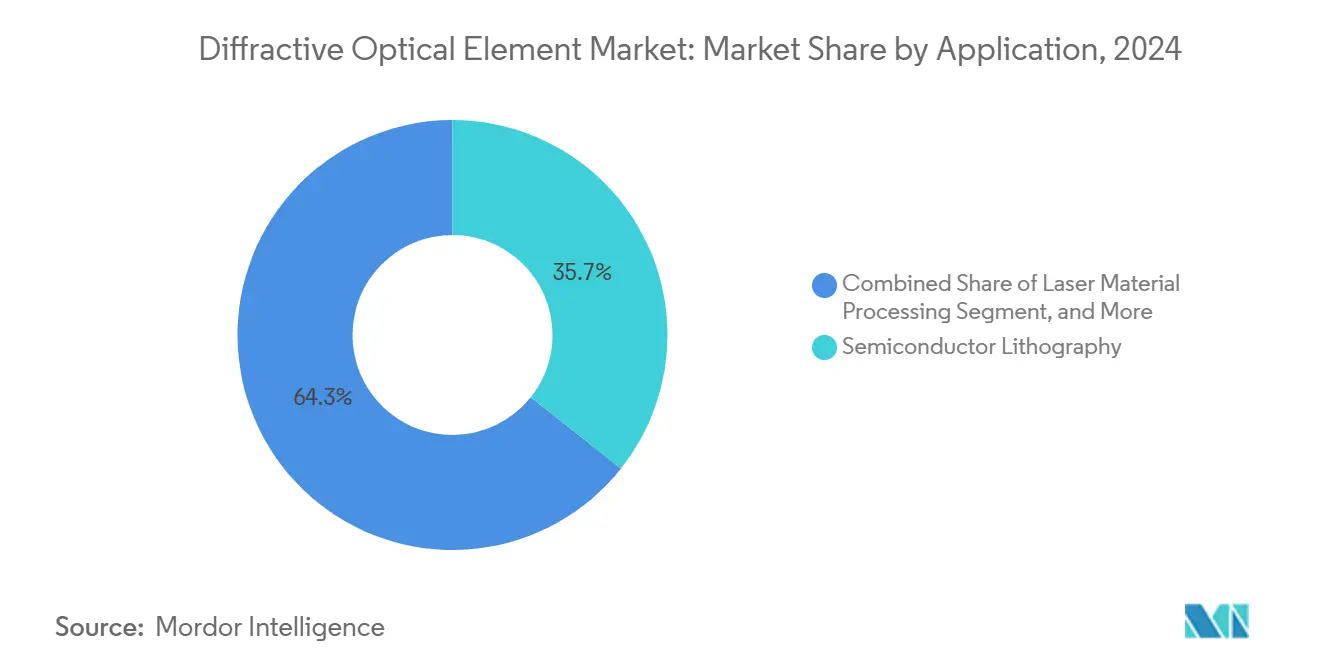
- By application, semiconductor lithography accounted for a 35.67% share of the diffractive optical element market size in 2024. Automotive LiDAR and ADAS is advancing at a 10.74% CAGR through 2030.
- By material, fused silica led with 43.89% revenue share in 2024. Gallium nitride is forecast to grow at an 11.42% CAGR to 2030.
- By end-use industry, semiconductor and electronics commanded 39.67% of revenue in 2024. Automotive applications are set to rise at a 9.89% CAGR between 2025-2030.
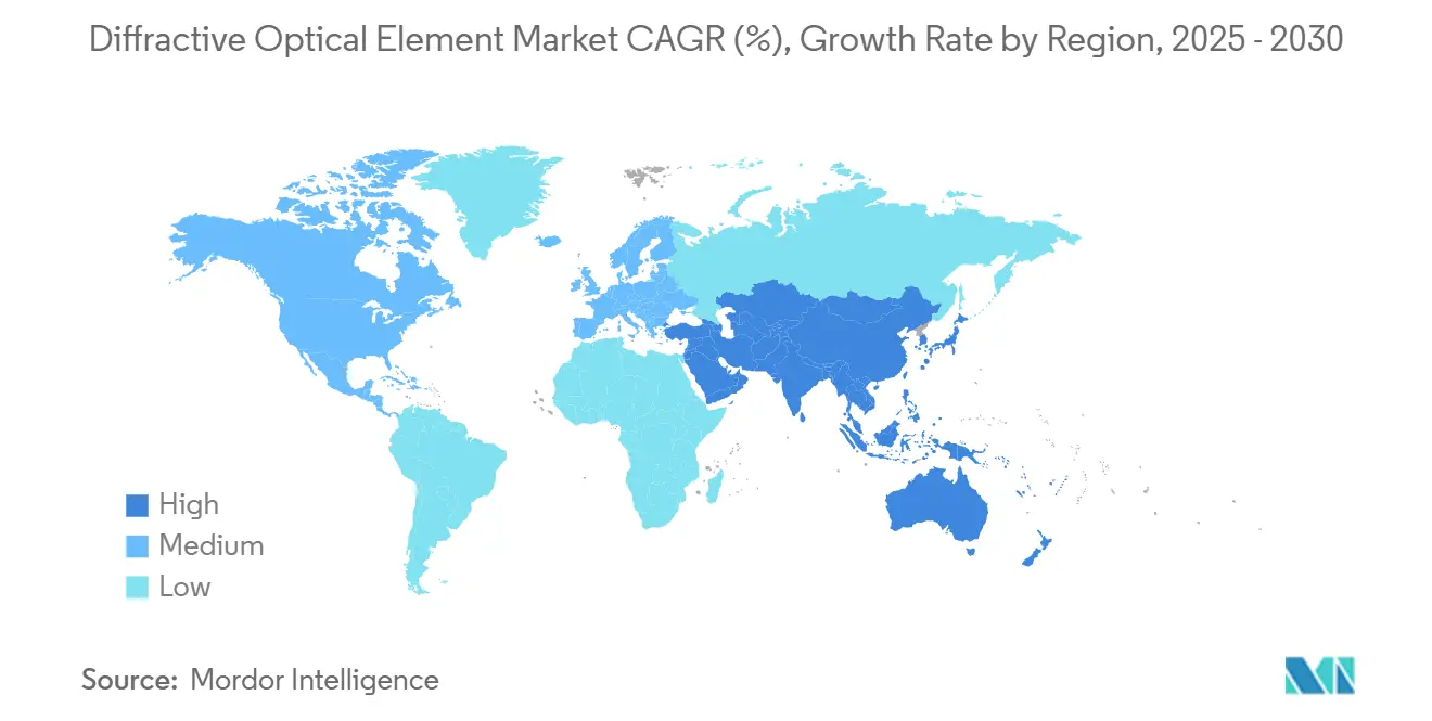
- By geography, Asia-Pacific captured 45.23% of sales in 2024, while the same region is poised to record a 10.39% CAGR over the outlook period.
Global Diffractive Optical Element Market Trends and Insights
Drivers Impact Analysis*
| Driver | (~) % Impact on CAGR Forecast | Geographic Relevance | Impact Timeline |
|---|---|---|---|
| Accelerated EUV lithography node migration | +2.1% | Taiwan, South Korea, Netherlands, United States | Medium term (2-4 years) |
| High-power fiber-laser beam homogenization for EV battery welding | +1.8% | China, Germany, United States | Short term (≤ 2 years) |
| Structured-light 3D sensing modules in smartphones | +1.6% | Asia-Pacific manufacturing hubs | Short term (≤ 2 years) |
| Standardized DOE libraries in photonic integrated circuits | +1.2% | North America, Europe, Asia-Pacific | Medium term (2-4 years) |
| Metasurface DOEs in solid-state automotive LiDAR | +1.4% | North America, Europe, Asia-Pacific | Medium term (2-4 years) |
| Spaceborne optical phased-array antennas | +0.8% | North America, Europe, Asia-Pacific | Long term (≥ 4 years) |
| Source: Mordor Intelligence | |||
Accelerated EUV Lithography Node Migration
Foundries scaling to 3 nm and below require sub-nanometer surface accuracy in diffractive gratings that condition 13.5 nm EUV light. Each ASML EUV scanner integrates multiple DOEs for beam shaping, flare suppression, and mask inspection. Taiwan Semiconductor Manufacturing Company plans to operate 20 EUV tools in 2025, elevating regional demand for ultra-clean fused-silica substrates. Incremental tool purchases by Samsung and Intel sustain global volume growth, while European optics firms secure multi-year purchase orders tied to capacity expansions.
High-Power Fiber-Laser Beam Homogenization for EV Battery Welding
Laser welding of prismatic and cylindrical cells relies on diffractive beam homogenizers that spread kilowatt-class energy uniformly across tab surfaces. Tesla’s Gigafactory integration of 4680 cell lines illustrates industry scale-up, prompting tier-one suppliers to validate 1,064 nm fused-silica homogenizers rated above 8 kW continuous power. [1]TRUMPF Group, “Laser Welding Solutions for EV Batteries,” TRUMPF.COM German automakers replicate similar processes for pouch cells, accelerating near-term shipment growth.
Structured-Light 3D Sensing Modules in Smartphones
Flagship devices adopt compact projector assemblies where metasurface DOEs split infrared beams into tens of thousands of dots for face authentication and augmented-reality depth capture. Apple’s Face ID roadmap and Meta’s smart-glasses prototypes depend on flat optics that maintain efficiency under 3 mm thickness constraints. Asian contract manufacturers extend capacity for wafer-level nanoimprint lithography, enhancing cost competitiveness for Android OEMs.
Standardized DOE Libraries in Photonic Integrated Circuits
Open-access design kits from AIM Photonics now include verified diffractive beam splitters, steering elements, and polarization converters. Device designers drag-and-drop pre-qualified cells, avoiding costly custom etch development and accelerating time-to-market for 800G and 1.6 Tbps transceiver modules. [2]American Institute for Manufacturing Integrated Photonics, “PDK Release Notes,” AIMPHOTONICS.COMFoundry adoption of library revisions every six months sustains a pipeline of incremental functionality and supports multi-project wafer subscriptions.
Restraints Impact Analysis*
| Restraint | (~) % Impact on CAGR Forecast | Geographic Relevance | Impact Timeline |
|---|---|---|---|
| Limited foundry capacity for large-area fused-silica etching | -1.5% | Global specialty foundries | Short term (≤ 2 years) |
| High qualification costs in medical laser endoscopy optics | -0.8% | North America, Europe | Medium term (2-4 years) |
| IP fragmentation around binary phase patterns | -0.6% | Global multi-jurisdiction | Long term (≥ 4 years) |
| Thermal stability limits of polymer DOEs in harsh-environment LiDAR | -0.9% | Global automotive and aerospace | Medium term (2-4 years) |
| Source: Mordor Intelligence | |||
Limited Foundry Capacity for Large-Area Fused-Silica Etching
Meter-scale gratings used in laser-fusion experiments exceed common lithography tool footprints. Only a handful of facilities can etch 1 m × 0.5 m plates to sub-75 nm depth tolerance, and backlogs stretch beyond 12 months. The National Ignition Facility booked nearly all 2025 slot capacity, limiting availability for space-borne telescope programs.
High Qualification Costs in Medical Laser Endoscopy Optics
FDA 510(k) submissions for novel diffractive tip optics require extensive biocompatibility, sterilization, and photothermal testing. Compliance fees and clinical data collection can raise unit development costs by USD 0.5 million, discouraging smaller suppliers. [3]U.S. Food and Drug Administration, “510(k) Premarket Notification Overview,” FDA.GOV European MDR rules add parallel documentation layers, extending time-to-market and dampening near-term adoption.
*Our forecasts treat driver/restraint impacts as directional, not additive. The impact forecasts reflect baseline growth, mix effects, and variable interactions.
Segment Analysis
By Product Type: Beam Shaping Elements Anchor Revenue
Beam shaping components accounted for 36.52% of revenue in 2024 and remain core to semiconductor lithography steppers and high-precision cutting lasers. Diffraction-limited top-hat generators deliver consistent dose uniformity that mitigates localized thermal gradients during wafer exposure. Beam splitters and diffusers supply display backlighting and ophthalmic surgery systems, sustaining steady demand. Vortex phase plates represent the fastest rising category with a 10.13% CAGR, enabled by quantum communication links that encode orbital angular momentum states and microscopy methods that improve resolution below the diffraction limit. The diffractive optical element market benefits from single-point diamond turning advances that polish fused-silica masters to 5 nm roughness. Nanostencil imprint tools now pattern multi-level phase features at 1,000 wafer-per-hour throughput, driving economies of scale. Emerging binary superpixel architectures demonstrate 1.44 kHz refresh capability, supporting dynamic holographic displays for next-generation headsets.
Continued R&D investment bolsters product breadth. Automotive LiDAR suppliers co-develop metasurface beam steering units with foundries to eliminate mechanical scanners. Medical device OEMs request hermetically-sealed beam shapers resistant to repeated autoclave cycles. Defense integrators specify radiation-hardened gratings for satellite laser communications. Each niche pushes vendors to expand design libraries and secure material supply agreements. The diffractive optical element market records rising multi-year framework contracts as customers lock capacity for critical nodes.


By Material: Fused Silica Retains Leadership
Fused silica commanded 43.89% share in 2024 due to its 0.55 ppm/K thermal expansion and low absorption at deep-ultraviolet wavelengths. These attributes are indispensable for 13.5 nm EUV beam conditioning where surface figure drift must remain below 50 pm. Gallium nitride is the fastest growing material with an 11.42% CAGR. Its high refractive index enables sub-wavelength metasurface designs that deliver broadband phase control while tolerating 250 °C operating temperatures. Silicon and quartz substrates satisfy CMOS back-end integration and birefringent filtering needs, respectively. Polymer surfaces including PMMA achieve high replication yields for consumer camera diffractive lenses but face outgassing and deformation limits in vehicle engine bays.
Material suppliers expand melt-drawing capacity for ultra-low OH- content silica blanks, while epitaxy vendors trial 200 mm GaN-on-sapphire growth for optics. Flexible nanoimprint lithography reduces per-lens costs by 30%, fostering uptake in augmented-reality modules. The diffractive optical element market observes R&D toward gallium phosphide and diamond substrates targeting vacuum ultraviolet astronomy and high-power directed energy systems, yet commercialization sits beyond the forecast horizon.
By Application: Semiconductor Lithography Dominates Precision Demand
Semiconductor lithography held 35.67% revenue share in 2024. Each EUV scanner employs dozens of beam homogenizers, pupil filters, and phase shifters to maintain critical dimension uniformity below 1.4 nm. Process node migrations sustain long-term replacement cycles and drive specialty order flow. Automotive LiDAR and ADAS exhibit the fastest CAGR at 10.74%. Solid-state LiDAR architecture replaces rotating mirrors with planar diffractive beam steering stacks, lowering parts count and improving shock resistance. Telecommunications and datacom employ standardized splitters in co-packaged optics reaching 1.6 Tbps, expanding volume baseline. Medical imaging, including ophthalmic OCT and endoscopy, integrates custom DOEs to enhance contrast and reduce form factor. High-power material processing lasers continue to adopt top-hat generators that improve cut edge quality in 6 mm stainless steel plate.
Silicon photonics merges optical and electronic functionality, allowing monolithic integration of small-footprint diffractive elements. AI accelerators leveraging photonic tensor cores generate a pipeline for specialized phase shifters and interferometers. The diffractive optical element market size for AI datacenters is projected to climb steadily as energy budgets push co-packaged optics adoption.
By End-Use Industry: Semiconductor Electronics Preserve Volume Leadership
The semiconductor and electronics sector accounted for 39.67% of shipments in 2024. EUV tool purchases, wafer inspection platforms, and advanced packaging lines account for bulk demand. Automotive applications show a 9.89% CAGR, aided by electric vehicle penetration and autonomy investments. Precision optics ensure battery welding consistency and LiDAR reliability under vibration and temperature extremes. Healthcare equipment maintains mid-single-digit growth through adoption of minimally invasive surgery tools and ocular implants. Defense programs fund spaceborne laser communications and directed energy research, creating low-volume, high-margin demand. Industrial manufacturing, including additive manufacturing and glass processing, rounds out the customer mix.
Tier-one automotive suppliers negotiate multi-year supply agreements that include performance guarantees over −40 °C to 125 °C cycles. Medical OEMs emphasize ISO-13485 certified production lines. Semiconductor customers prioritize sub-0.3 nm repeatability in critical surface features. Meeting diverse specifications compels vendors to widen metrology capabilities and implement advanced statistical process controls. The diffractive optical element market therefore shows balanced exposure across cyclical and secular growth end markets.
Geography Analysis
Asia-Pacific’s diffractive optical element market represent 45.23% of global demand. Robust 10.39% CAGR through 2030 aligns with continued wafer-fab expansion in Taiwan and mainland China, as well as Japanese leadership in precision metrology. Government incentives such as China’s “Photonics Valley” program earmark multi-year grants for metasurface pilot lines, while Japan’s NEDO funds EUV resist research that needs custom diffractive masks. South Korea’s memory makers and display panel fabs secure local optics to shorten logistics chains. Regional vendors benefit from vertically integrated supply chains that co-locate wafer polishing, photolithography, and thin-film coating, lowering unit costs and enabling rapid prototyping. International customers tap the region for cost-competitive high-mix low-volume batches.
North America commands strong positions in defense, aerospace, and data-center optics. U.S. laser fusion projects at Lawrence Livermore National Laboratory order large-aperture gratings that few global shops can make. Silicon Valley photonics startups leverage venture funding to commercialize GaN metasurfaces for AR/VR headsets. Canada’s quantum computing research institutes partner with local optics firms on photon-based qubit manipulation, adding niche orders. Mexico’s emerging EV supply chain imports beam shaping units for battery welding lines, inserting incremental volume into regional flow. Regional collaboration programs link universities with defense primes, ensuring workforce development in nano-fabrication skills.
Europe accounts for 24.5% of worldwide consumption. German automakers accelerate LiDAR integration in Level-3 driver-assistance systems, driving demand for high-efficiency metasurface beam steering parts. The Netherlands’ ASML anchors a cluster of optical suppliers proficient in deep-ultraviolet metrology. French aerospace primes procure space-qualified gratings for telecommunication satellite constellations. The new EU Medical Device Regulation elevates compliance overhead, encouraging consolidation among small-and-medium optics workshops. Joint research initiatives such as Horizon Europe fund quantum photonics programs that consume vortex plates and binary phase elements. The region’s mature quality standards position suppliers to address high-reliability sectors but add cost pressure versus Asian peers.
Middle East and Africa remain nascent, collectively below 3% share. Yet sovereign investment funds in the Gulf pursue semiconductor diversification that may trigger greenfield fabs with localized optics purchasing. South Africa’s astronomy installations, including the Square Kilometer Array, require specialized diffractive elements for adaptive optics experiments, providing modest high-value orders.

Competitive Landscape
The diffractive optical element market features moderate concentration. The top five vendors control an estimated 46% of global revenue, balancing scale advantages against a vibrant field of niche innovators. Jenoptik grows through vertical integration that covers blank production, lithography, and anti-reflective coatings. HOLOEYE leverages proprietary design software to deliver rapid-turn custom spatial light modulators. Holo/Or maintains a robust patent portfolio in beam shaping, securing multi-year supply contracts with laser tool OEMs.
Metasurface startups aim to disrupt incumbents by depositing nano-pillar arrays via high-throughput etching. Surfaced-etched flat lenses promise 30% lower weight and improved thermal stability for smart-phone depth cameras. Patent filings in 2024 grew 12% year on year, reflecting race conditions around automotive waveguide and AR headset optics. Consolidation continues, as Teledyne’s USD 710 million acquisition of Excelitas business units extends reach into medical and industrial sectors, while G&H’s purchase of Phoenix Optical adds high-power grating capability.
Supply-chain vulnerabilities in ultra-low-defect fused-silica remain pinch points. Vendors sign multi-year take-or-pay contracts to secure furnace slots. Regionalization strategies see U.S. and European customers qualifying secondary sources to mitigate geopolitical risk. Compliance with IEC 60825-1 laser safety standards increases documentation requirements but favors established players with mature quality systems. Competitive differentiation focuses on application-specific expertise, metrology automation, and end-to-end modeling support that shorten customer design cycles.
Diffractive Optical Element Industry Leaders
Jenoptik AG
Holo/Or Ltd.
HOLOEYE Photonics AG
LightTrans International UG
Edmund Optics, Inc.
- *Disclaimer: Major Players sorted in no particular order

Recent Industry Developments
- June 2025: LASER World of Photonics forum spotlighted projected USD 100 billion fusion-energy optics demand, emphasizing large-area fused-silica supply challenges.
- April 2025: ISO released new guidelines for presbyopia-correcting intraocular lenses, tightening clinical evidence standards.
- March 2025: POET Technologies demonstrated an optical interposer reaching 1.6 Tbps and 3.2 Tbps data rates for AI clusters.
- February 2025: Researchers achieved 100 nm resolution laser writing on glass using dual-beam setups, accelerating micro-optics fabrication.


Global Diffractive Optical Element Market Report Scope
| Beam Shaping Elements |
| Beam Splitters |
| Diffusers / Homogenisers |
| Vortex / Spiral Phase Plates |
| Grating-based DOEs |
| Fused Silica |
| Quartz |
| Silicon |
| Gallium Nitride |
| Polymers (PMMA, PC) |
| Laser Material Processing |
| Semiconductor Lithography |
| Medical and Life-Science Imaging |
| Telecommunications and Datacom |
| Automotive LiDAR and ADAS |
| Semiconductor and Electronics |
| Healthcare |
| Automotive |
| Defense and Aerospace |
| Industrial Manufacturing |
| North America | United States | |
| Canada | ||
| Mexico | ||
| South America | Brazil | |
| Argentina | ||
| Rest of South America | ||
| Europe | Germany | |
| United Kingdom | ||
| France | ||
| Russia | ||
| Rest of Europe | ||
| Asia-Pacific | China | |
| Japan | ||
| India | ||
| South Korea | ||
| Australia | ||
| Rest of Asia-Pacific | ||
| Middle East and Africa | Middle East | Saudi Arabia |
| United Arab Emirates | ||
| Rest of Middle East | ||
| Africa | South Africa | |
| Egypt | ||
| Rest of Africa | ||
| By Product Type | Beam Shaping Elements | ||
| Beam Splitters | |||
| Diffusers / Homogenisers | |||
| Vortex / Spiral Phase Plates | |||
| Grating-based DOEs | |||
| By Material | Fused Silica | ||
| Quartz | |||
| Silicon | |||
| Gallium Nitride | |||
| Polymers (PMMA, PC) | |||
| By Application | Laser Material Processing | ||
| Semiconductor Lithography | |||
| Medical and Life-Science Imaging | |||
| Telecommunications and Datacom | |||
| Automotive LiDAR and ADAS | |||
| By End-Use Industry | Semiconductor and Electronics | ||
| Healthcare | |||
| Automotive | |||
| Defense and Aerospace | |||
| Industrial Manufacturing | |||
| By Geography | North America | United States | |
| Canada | |||
| Mexico | |||
| South America | Brazil | ||
| Argentina | |||
| Rest of South America | |||
| Europe | Germany | ||
| United Kingdom | |||
| France | |||
| Russia | |||
| Rest of Europe | |||
| Asia-Pacific | China | ||
| Japan | |||
| India | |||
| South Korea | |||
| Australia | |||
| Rest of Asia-Pacific | |||
| Middle East and Africa | Middle East | Saudi Arabia | |
| United Arab Emirates | |||
| Rest of Middle East | |||
| Africa | South Africa | ||
| Egypt | |||
| Rest of Africa | |||


Key Questions Answered in the Report
What is the projected value of the diffractive optical element market in 2030?
The market is expected to reach USD 491.36 million by 2030, growing at a 9.53% CAGR.
Which region leads global demand for diffractive optical elements?
Asia-Pacific held 45.23% of global revenue in 2024 and shows the fastest growth at 10.39% CAGR through 2030.
Which application segment is expanding most rapidly?
Automotive LiDAR and ADAS applications exhibit the highest growth, registering a 10.74% CAGR during 2025-2030.
Why is gallium nitride gaining traction as a substrate material?
GaN offers a high refractive index and thermal tolerance, driving an 11.42% CAGR by enabling compact metasurface designs for high-power lasers.
What is the main restraint affecting near-term supply?
Limited foundry capacity for large-area fused-silica etching extends lead times beyond 12 months for meter-scale components.
How concentrated is vendor competition?
The top five companies control roughly 46% of global revenue, indicating a moderately concentrated landscape with space for emerging specialists.
Page last updated on:


