Co-packaged Optics Market Size and Share
Market Overview
| Study Period | 2020 - 2031 |
|---|---|
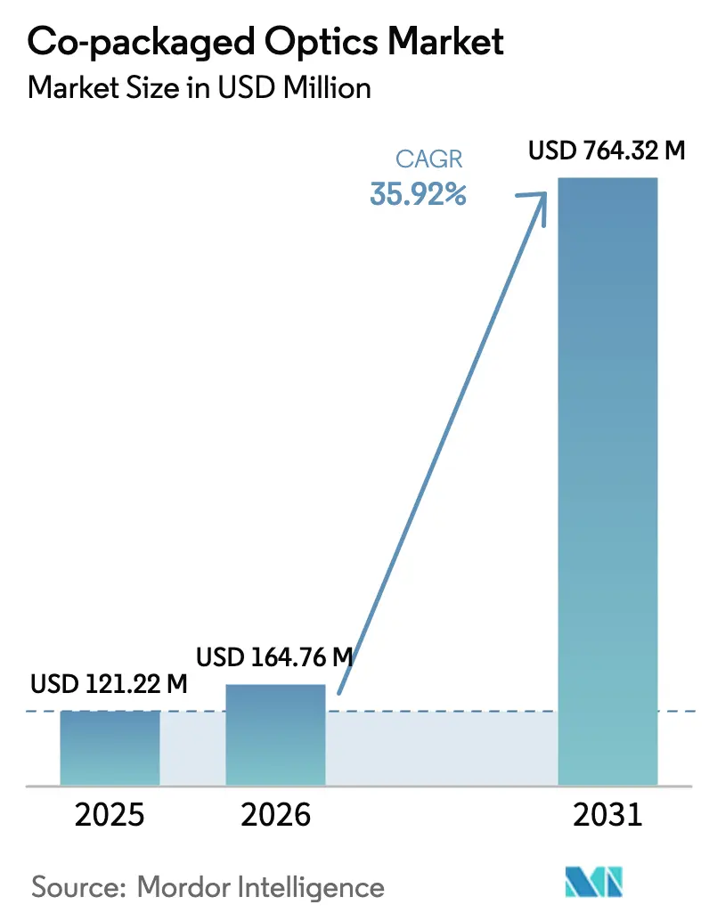
| Market Size (2026) | USD 164.76 Million |
| Market Size (2031) | USD 764.32 Million |
| Growth Rate (2026 - 2031) | 35.92% CAGR |
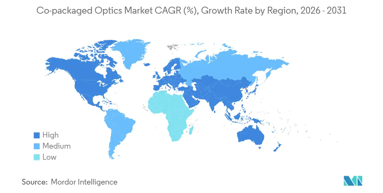
| Fastest Growing Market | Asia Pacific |
| Largest Market | North America |
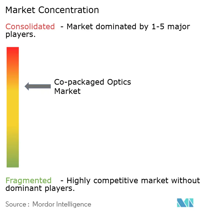
| Market Concentration | Medium |
Major Players *Disclaimer: Major Players sorted in no particular order Image © Mordor Intelligence. Reuse requires attribution under CC BY 4.0. | |
Co-packaged Optics Market Analysis by Mordor Intelligence
The co-packaged optics market size is projected to be USD 121.22 million in 2025, USD 164.76 million in 2026, and reach USD 764.32 million by 2031, growing at a CAGR of 35.92% from 2026 to 2031. Surging switch-silicon bandwidth, stricter energy-efficiency mandates, and the thermal ceiling of 800 G and 1.6 T pluggables are accelerating the adoption of switch-integrated photonics. Foundry participation led by TSMC is unlocking volume economics that were previously unattainable in boutique silicon photonics runs. Early revenue shipments from Broadcom’s second-generation Tomahawk 5-Bailly switches confirm that the technology has left the prototype phase and entered mainstream deployment. At the same time, vertically integrated device makers are capturing system-level value, squeezing margins for standalone transceiver vendors. Finally, open hardware specifications published by the Open Compute Project are lowering vendor lock-in risks and encouraging multi-source strategies.
Key Report Takeaways
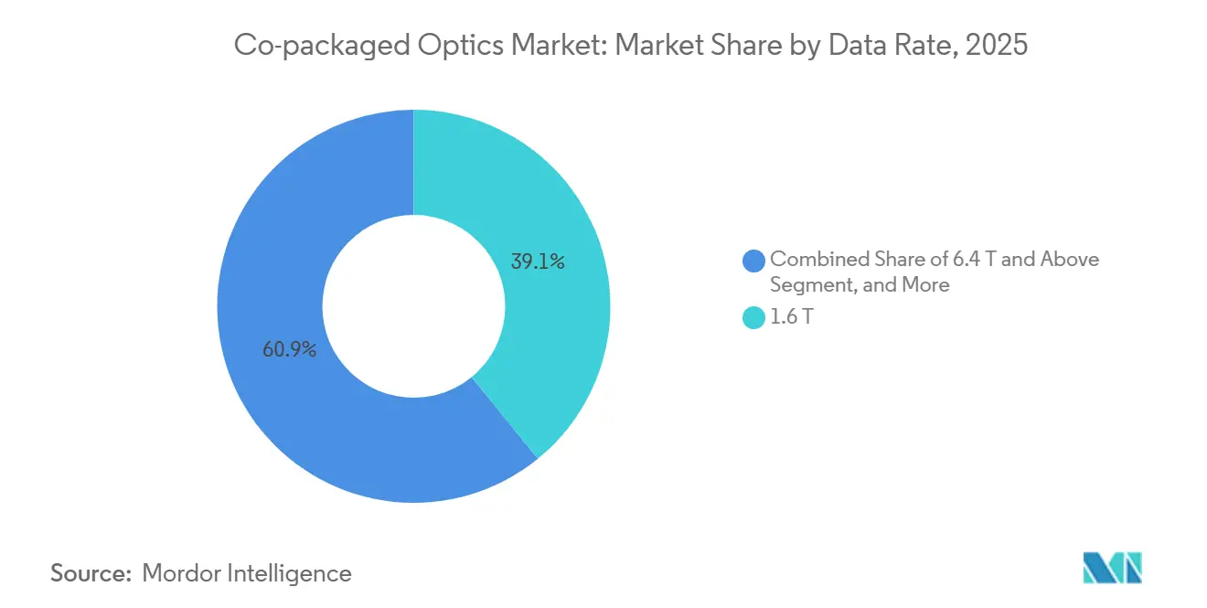
- By data rate, 1.6 T commanded 39.12% share of the co-packaged optics market in 2025, while the 6.4 T and above segment is forecast to grow at a 36.69% CAGR through 2031.
- By component, optical engines led with 43.76% revenue share in 2025; laser sources are advancing at a 36.89% CAGR during 2026-2031.
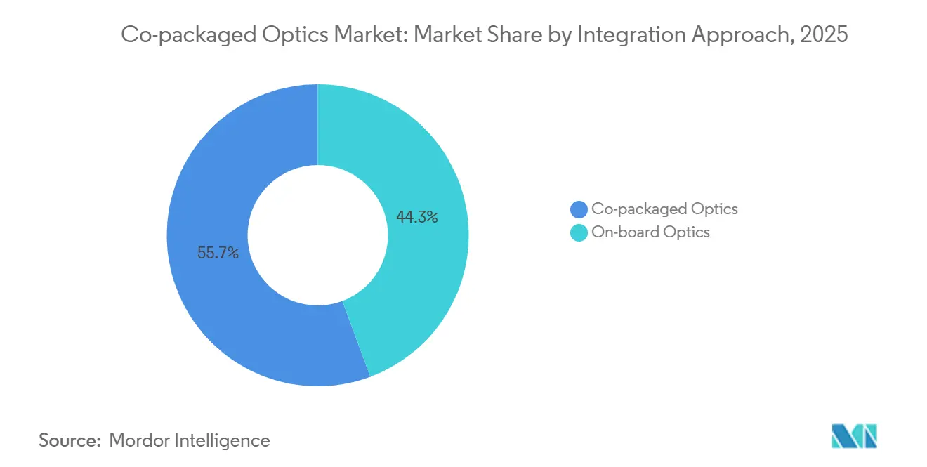
- By integration approach, co-packaged architectures captured a 55.67% share in 2025 and are projected to expand at a 36.17% CAGR to 2031.
- By end use, hyperscale cloud data centers held a 62.34% share in 2025, whereas HPC and AI/ML clusters are expected to grow at a 36.96% CAGR over the forecast period.
- By geography, North America accounted for a 47.83% share in 2025; Asia Pacific is set to grow at a 36.91% CAGR, the highest among all regions.
Note: Market size and forecast figures in this report are generated using Mordor Intelligence’s proprietary estimation framework, updated with the latest available data and insights as of 2026.
Global Co-packaged Optics Market Trends and Insights
Drivers Impact Analysis*
| Driver | (~) % Impact on CAGR Forecast | Geographic Relevance | Impact Timeline |
|---|---|---|---|
| Ramp-up of 51.2 T switch silicon requiring 1.6 T CPO | +7.2% | North America and Asia Pacific core, spill-over to Europe | Short term (≤ 2 years) |
| Hyperscale data-center energy-efficiency mandates | +6.8% | Global, with early enforcement in North America and EU | Medium term (2-4 years) |
| Surge in AI/ML cluster bandwidth demand | +8.1% | North America and Asia Pacific, concentrated in hyperscaler regions | Short term (≤ 2 years) |
| Transition to 800 G/1.6 T pluggables hitting thermal limits | +5.9% | Global | Short term (≤ 2 years) |
| Foundry participation enabling volume economics | +4.7% | Asia Pacific core, with TSMC Taiwan and secondary nodes in North America | Medium term (2-4 years) |
| Open Compute-driven CPO collaboration reducing vendor lock-in | +3.5% | Global, with strongest adoption in North America hyperscalers | Long term (≥ 4 years) |
| Source: Mordor Intelligence | |||
Ramp-Up of 51.2 T Switch Silicon Requiring 1.6 T CPO
Second-generation 51.2 T switch ASICs integrate 64 ports of 800 G optics to sustain radix within a single rack unit.[1]Broadcom Inc., “Broadcom Tomahawk 5 Technology Brief,” broadcom.com Broadcom’s Tomahawk 5-Bailly platform ships in volume, proving manufacturability at 100 G per lane. NVIDIA’s Quantum-X800 InfiniBand device delivers 144 ports of 800 G with only 4 dB insertion loss, a 63-fold eye-opening improvement over pluggables. Hyperscalers have pre-allocated foundry capacity through multi-year purchase commitments, effectively locking in demand. The architecture also lets operators collapse spine tiers, cutting capital expenditure per terabit. Sampling of 102.4 T silicon in late 2026 will pull 3.2 T and 6.4 T co-packaged interfaces into qualification cycles.
Hyperscale Data-Center Energy-Efficiency Mandates
The United States data-center power draw is projected to scale from 176 TWh in 2023 to as high as 580 TWh by 2028, with networking already near 23 TWh.[2]Lawrence Berkeley National Laboratory, “United States Data Center Energy Usage 2023-2028,” lbl.gov Co-packaged optics remove retimers and DSP stages, lowering per-port power by 30-40% at 800 G-plus speeds. Operators in power-constrained campuses now include “watts per terabit” in vendor scorecards, while EU directives embed efficiency metrics into tender documents. By reducing thermal load at the faceplate, co-packaged designs defer expensive electrical infrastructure upgrades. Regulatory pressure to curb carbon emissions is turning energy-efficient interconnects from an optimization lever into a procurement prerequisite.
Surge in AI/ML Cluster Bandwidth Demand
Training runs for trillion-parameter models saturate conventional three-tier Clos fabrics. NVIDIA’s DGX SuperPOD specifies 3.2 T of bi-directional bandwidth for every GPU, a figure that will double with next-generation accelerators.[3]NVIDIA Corporation, “Quantum-X800 Technical Architecture,” nvidia.com Rail-optimized topologies become feasible when port density and power envelopes align, a balance enabled by co-packaged optics. Meta’s AI Research SuperCluster shaved 18% off training time for a 175-billion-parameter model after migrating from pluggable to 800 G co-packaged links. As real-time inference spreads to autonomous vehicles and interactive agents, latency budgets continue to tighten, boosting demand for integrated photonics.
Transition to 800 G - 1.6 T Pluggables Hitting Thermal Limits
OSFP and QSFP-DD modules cap heat dissipation near 18 W. Climbing to 1.6 T requires 200 G lanes, PAM4 modulation, and tighter FEC overhead, which raise bit-error rates beyond forward-error thresholds on moderate-reach links. Co-packaged engines distribute thermal load onto the ASIC heatsink, where vapor chambers and embedded heat pipes operate unconstrained by front-panel mechanics. Broadcom’s third-generation roadmap moves to 200 G lanes and charts a path toward 400 G lanes, a trajectory that pluggables cannot replicate without radical form-factor change.
Restraints Impact Analysis*
| Restraint | (~) % Impact on CAGR Forecast | Geographic Relevance | Impact Timeline |
|---|---|---|---|
| Manufacturing complexity and heterogeneous-integration yield | -4.3% | Global, with acute impact in North America and Europe due to limited foundry capacity | Short term (≤ 2 years) |
| Interoperability and standards immaturity | -3.1% | Global | Medium term (2-4 years) |
| Shift of optical-module ownership to switch-ASIC vendors | -2.6% | Global, with concentrated impact on traditional optical-module suppliers in Asia Pacific | Medium term (2-4 years) |
| Photonic-packaging workforce skills gap | -1.9% | North America and Europe, with emerging impact in Asia Pacific | Long term (≥ 4 years) |
| Source: Mordor Intelligence | |||
Manufacturing Complexity and Heterogeneous-Integration Yield
Bonding III-V lasers, silicon-photonic waveguides, and CMOS logic within one package requires sub-micron alignment tolerance. Several foundries reported yields under 70% as of early 2026, inflating unit cost for all but the densest switches. TSMC’s early COUPE production targets 60-65% yield, implying 35-40% scrap. Advanced metrology, such as optical coherence tomography, is improving process control, yet the learning curve remains steeper than for electronic packaging. Until yields cross the high-80% threshold, enterprise and telco deployments will continue favoring legacy pluggables on a pure cost basis.
Interoperability and Standards Immaturity
The Open Compute Project released a mechanical spec in 2025, but wavelength grids, modulation formats, and FEC schemes still vary by customer. IEEE 802.3 groups expect to ratify co-packaged Ethernet at 800 G and 1.6 T only in late 2027. In the interim, every hyperscaler qualifies modules against bespoke test plans, limiting second-source viability. The Optical Internetworking Forum has proposed interoperability suites, yet participation is voluntary, and coverage is incomplete. Vendor-specific paths risk marooning early deployments on incompatible islands.
*Our forecasts treat driver/restraint impacts as directional, not additive. The impact forecasts reflect baseline growth, mix effects, and variable interactions.
Segment Analysis
By Data Rate: 6.4 T Interfaces Anchor Next-Generation Fabrics
In 2025, the 1.6 T segment captured a dominant 39.12% of the co-packaged optics market, while projections indicate that the segment of 6.4 T and above is set to expand at a robust CAGR of 36.69% through 2031. Early movers such as Tomahawk 5 and Quantum-X800 standardize on 2x800G breakouts or 16x100G lanes. Rapid sampling of 102.4 T silicon means 3.2 T and 6.4 T ports will dominate qualification roadmaps during 2026-2028. Operators with legacy 400 G fiber plants continue to use below-1.6 T links in brownfield upgrades, but new hyperscale builds prioritize port densities that only higher-rate optics enable.
TSMC’s mass-production COUPE flow supports up to 6.4 T per package by integrating modulators and detector arrays into a single interposer. Intel’s roadmap echoes this trajectory, aiming for 6.4 T by 2027 with monolithically integrated lasers. As AI cluster node counts balloon, network architects value bisection bandwidth over incremental cost, driving a secular mix-shift toward 6.4 T and above. Consequently, the 6.4 T cohort is forecast to capture an outsized share of the co-packaged optics market between 2028 and 2031.


By Component: Integrated Laser Sources Accelerate
Optical engines led the revenue stack at 43.76% in 2025, consolidating modulation, detection, and multiplexing on silicon. The laser-source category is set to post a 36.89% CAGR, the quickest among components, once heterogeneous III-V bonding matures. Coherent’s indium-phosphide designs target sub-500 mW per wavelength, unlocking new cost curves. Lumentum’s quantum-dot arrays improve wavelength uniformity, addressing reliability needs inside thermally turbulent switch enclosures.
Electrical IC content shrinks per port as SerDes functions co-locate within the switch die. Packaging and connector innovations, such as 64-fiber MPOs, raise panel density without sacrificing insertion loss. Miscellaneous passive components remain incremental plays. Over the forecast period, greater integration of lasers into the photonic stack is expected to lift the laser segment’s share of the overall co-packaged optics market.
By Integration Approach: Co-Packaged Dominates New Designs
Co-packaged architectures held a 55.67% share in 2025 and will widen their lead, growing at a 36.17% CAGR to 2031. By directly linking switch SerDes blocks to photonic modulators, engineers have shortened the electrical path length to under 1 mm, ensuring eye margins are maintained at 100 G lanes. NVIDIA's Quantum-X800 integrates 144 ports of 800G optics within its package, doing away with the requirement for a separate retimer power.
On-board optics remain serviceable for enterprise and telco workloads that value module swaps, yet their added latent heat and trace loss impose penalties at 200 G and beyond. Ayar Labs’ optical-interposer chiplet approach offers a middle ground, enabling mix-and-match integration while still qualifying as co-packaged. As yields rise and cost deltas narrow, co-packaged solutions will dominate incremental port additions, reinforcing their leadership in the co-packaged optics market.
By End-Use Application: HPC and AI/ML Clusters Accelerate
Hyperscale cloud data centers captured 62.34% of revenue in 2025, driven by the concentrated buying power of four dominant operators. However, HPC and AI/ML clusters are expected to expand at a 36.96% CAGR, the swiftest among applications, as frontier model training requires near-line-rate, all-to-all fabrics. Meta’s SuperCluster improved training time by 18% after shifting to co-packaged optics, validating the upside in performance.
Enterprise data centers are selectively adopting the technology, with a keen focus on latency-sensitive sectors like financial trading. While telco central offices represent a smaller segment, they are placing a premium on 5G core densification. Catering to this specialized need, Nokia has introduced its carrier-grade CPO platform. Furthermore, clusters that alleviate network bottlenecks not only address server underutilization but also position integrated photonics as a significant return on investment lever.
Geography Analysis
North America accounted for 47.83% of 2025 revenue, anchored by U.S. hyperscalers and CHIPS Act grants that subsidize domestic photonics pilot lines. In 2024-2025, Intel, Ayar Labs, and a consortium of universities garnered a combined USD 280 million for their silicon photonics R&D endeavors. While the funding has a cross-border dimension, it's limited: Canada is home to connector assembly plants, and Mexico specializes in back-end testing and finishing.
Asia Pacific is forecast to log a 36.91% CAGR through 2031, the quickest globally. TSMC’s COUPE ramp offers immediate volume in Taiwan, while Japanese and South Korean firms add connector and laser capacity. Chinese vendors innovate around export-control constraints by integrating hybrid components into mature nodes. India and Australia offer greenfield data center incentives, yet front-end wafer production remains concentrated in Taiwan and Japan.
Europe, the Middle East, and Africa account for the balance. The EU Chips Act backs photonics research at IMEC and Fraunhofer, but limited high-volume foundry capacity caps regional output. Germany, the United Kingdom, and France host niche optical component suppliers that have yet to meet hyperscale cost curves. Middle Eastern sovereign clouds drive pockets of demand, while African adoption stays embryonic.

Competitive Landscape
The arena shows moderate concentration. Broadcom, NVIDIA, and Marvell secure most hyperscale sockets by vertically integrating switch silicon and photonics. Broadcom’s early engagements translated into 50,000-plus CPO switches shipped by 2025, squeezing standalone transceiver margins. NVIDIA leverages its GPU dominance to bundle Quantum-series networks, while Marvell’s Teralynx sampling widens customer choice.
Traditional module vendors face a squeeze: Coherent bought InnoLight to gain scale, and Sumitomo Electric is ramping 64-fiber connectors to defend its share. Ayar Labs and POET Technologies pursue chiplet-based white-label optics that slot into custom ASICs without full vertical stacks. Patents around wafer-level bonding and photonic wire-bonding raise barriers for new entrants, but open specifications may mitigate lock-in risks over time.
In the telco and enterprise segments, opportunities abound. Vendors offering "right-sized" optics, tailored and not overly specified for hyperscale needs, can find their niche. Ranovus is focusing on edge computing with its quantum-dot lasers. Meanwhile, Sicoya is championing European silicon photonics, emphasizing data center sovereignty in the region. As design victories become more concentrated and cost curves rise, a wave of consolidation seems imminent.
Co-packaged Optics Industry Leaders
Ayar Labs Inc.
Broadcom Inc.
Cisco Systems Inc.
Intel Corporation
TE Connectivity Ltd.
- *Disclaimer: Major Players sorted in no particular order

Recent Industry Developments
- February 2026: TSMC moved COUPE into risk production with AMD, targeting 6.4 T per package high-volume runs in 2H 2026.
- January 2026: Broadcom confirmed shipments of more than 50,000 Tomahawk 5-Bailly CPO switches during 2025 and previewed its 200 G-per-lane third-generation platform.
- November 2025: NVIDIA unveiled Quantum-X800 InfiniBand, integrating 144 ports of 800 G CPO and claiming a 63-fold signal-integrity gain versus OSFP modules.
- September 2025: Intel announced a USD 150 million expansion of its New Mexico silicon-photonics fab, slated to open in early 2027.


Global Co-packaged Optics Market Report Scope
The Co-packaged Optics Market Report is Segmented by Data Rate (Below 1.6 T, 1.6 T, 3.2 T, 6.4 T and Above), Component (Optical Engine, Electrical IC, Laser Source, Connector and Packaging, Other Components), Integration Approach (On-board Optics, and Co-packaged Optics), End-use Application (Hyperscale Cloud Data Centers, Enterprise Data Centers, Telco Central Offices, HPC and AI/ML Clusters, Other End-use Applications), and Geography (North America, South America, Europe, Asia Pacific, Middle East, Africa). The Market Forecasts are Provided in Terms of Value (USD).
| Below 1.6 T |
| 1.6 T |
| 3.2 T |
| 6.4 T and Above |
| Optical Engine |
| Electrical IC |
| Laser Source |
| Connector and Packaging |
| Other Components |
| On-board Optics |
| Co-packaged Optics |
| Hyperscale Cloud Data Centers |
| Enterprise Data Centers |
| Telco Central Offices |
| HPC and AI/ML Clusters |
| Other End-use Applications |
| North America | United States | |
| Canada | ||
| Mexico | ||
| South America | Brazil | |
| Argentina | ||
| Rest of South America | ||
| Europe | Germany | |
| United Kingdom | ||
| France | ||
| Italy | ||
| Russia | ||
| Rest of Europe | ||
| Asia Pacific | China | |
| Japan | ||
| South Korea | ||
| India | ||
| Australia | ||
| Rest of Asia Pacific | ||
| Middle East and Africa | Middle East | United Arab Emirates |
| Saudi Arabia | ||
| Turkey | ||
| Rest of Middle East | ||
| Africa | South Africa | |
| Egypt | ||
| Rest of Africa | ||
| By Data Rate | Below 1.6 T | ||
| 1.6 T | |||
| 3.2 T | |||
| 6.4 T and Above | |||
| By Component | Optical Engine | ||
| Electrical IC | |||
| Laser Source | |||
| Connector and Packaging | |||
| Other Components | |||
| By Integration Approach | On-board Optics | ||
| Co-packaged Optics | |||
| By End-use Application | Hyperscale Cloud Data Centers | ||
| Enterprise Data Centers | |||
| Telco Central Offices | |||
| HPC and AI/ML Clusters | |||
| Other End-use Applications | |||
| By Geography | North America | United States | |
| Canada | |||
| Mexico | |||
| South America | Brazil | ||
| Argentina | |||
| Rest of South America | |||
| Europe | Germany | ||
| United Kingdom | |||
| France | |||
| Italy | |||
| Russia | |||
| Rest of Europe | |||
| Asia Pacific | China | ||
| Japan | |||
| South Korea | |||
| India | |||
| Australia | |||
| Rest of Asia Pacific | |||
| Middle East and Africa | Middle East | United Arab Emirates | |
| Saudi Arabia | |||
| Turkey | |||
| Rest of Middle East | |||
| Africa | South Africa | ||
| Egypt | |||
| Rest of Africa | |||


Key Questions Answered in the Report
What is the projected value of the co-packaged optics market in 2031?
The market is forecast to reach USD 764.32 million by 2031.
Why are hyperscalers moving from pluggable to co-packaged optics?
Integrated photonics cut per-port power by around 30-40% and remove thermal limits that cap pluggable modules at 800 G.
Which data-rate segment will grow the fastest through 2031?
Interfaces at 6.4 T and above are expected to expand at a 36.69% CAGR.
Which region will show the highest growth in adoption?
Asia Pacific is set to grow at a 36.91% CAGR, driven by TSMC’s production ramp and regional component supply.
Who are the leading vendors in the space?
Broadcom, NVIDIA and Marvell hold the majority of hyperscale design wins, while Coherent and Ayar Labs are notable challengers.
What is the main manufacturing bottleneck today?
Heterogeneous-integration yields below 70% remain the chief headwind, elevating unit cost compared to legacy pluggables.
Page last updated on:


