Optical Waveguide Market Size and Share
Market Overview
| Study Period | 2020 - 2031 |
|---|---|
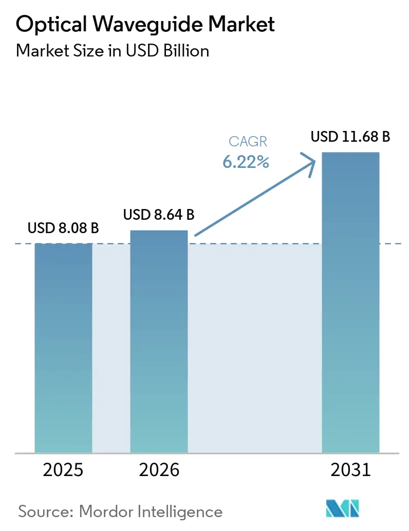
| Market Size (2026) | USD 8.64 Billion |
| Market Size (2031) | USD 11.68 Billion |
| Growth Rate (2025 - 2030) | 6.22% CAGR |
| Fastest Growing Market | Asia Pacific |
| Largest Market | Asia Pacific |
| Market Concentration | Low |
Major Players *Disclaimer: Major Players sorted in no particular order Image © Mordor Intelligence. Reuse requires attribution under CC BY 4.0. | |
Optical Waveguide Market Analysis by Mordor Intelligence
The optical waveguide market size is projected to expand from USD 8.08 billion in 2025 and USD 8.64 billion in 2026 to USD 11.68 billion by 2031, registering a CAGR of 6.22% between 2026 to 2031. Structural migration toward co-packaged optics is compressing the bill of materials by removing pluggable transceivers, thereby elevating demand for on-die waveguides embedded alongside switch ASICs. Semiconductor foundries are monetizing this pivot by opening 300-millimeter pilot lines that integrate silicon photonics and advanced packaging, while polymer waveguide suppliers accelerate time-to-market through low-temperature processing.[1] Telecommunications roll-outs for 25 gigabit-per-second passive optical networks keep legacy planar-lightwave-circuit volumes steady, yet hyperscale datacenter retrofits remain the single largest incremental revenue driver. Investment programs under the CHIPS Act, Photonics21, and multiple Asia-Pacific semiconductor funds ensure capital availability, but high lithography costs preserve moderate entry barriers that temper over-capacity risk.
Key Report Takeaways
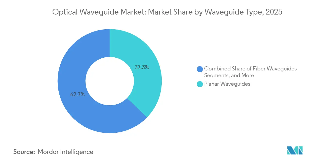
- By waveguide type, planar architectures led with 37.29% of the optical waveguide market share in 2025, while photonic-crystal designs are forecast to expand at a 7.11% CAGR through 2031.
- By material, glass and silica commanded 48.91% of the optical waveguide market share in 2025, whereas polymer waveguides are projected to grow at a 6.72% CAGR to 2031.
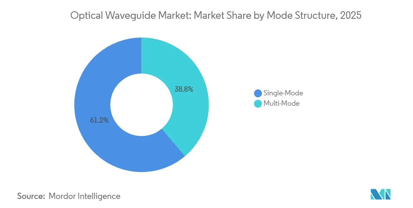
- By mode structure, single-mode designs held 61.19% share of the optical waveguide market share in 2025 and multi-mode configurations are advancing at a 6.85% CAGR to 2031.
- By application, telecommunications and datacom represented 43.43% of the optical waveguide market share in 2025, while consumer electronics and AR/VR are recording the highest projected CAGR at 6.94% through 2031.
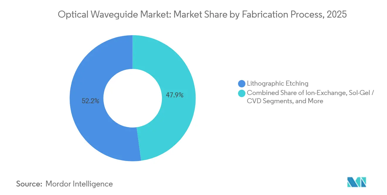
- By fabrication process, lithographic etching captured 52.15% of the optical waveguide market share in 2025, but ultrafast laser inscription is forecast to expand at a 7.06% CAGR to 2031.
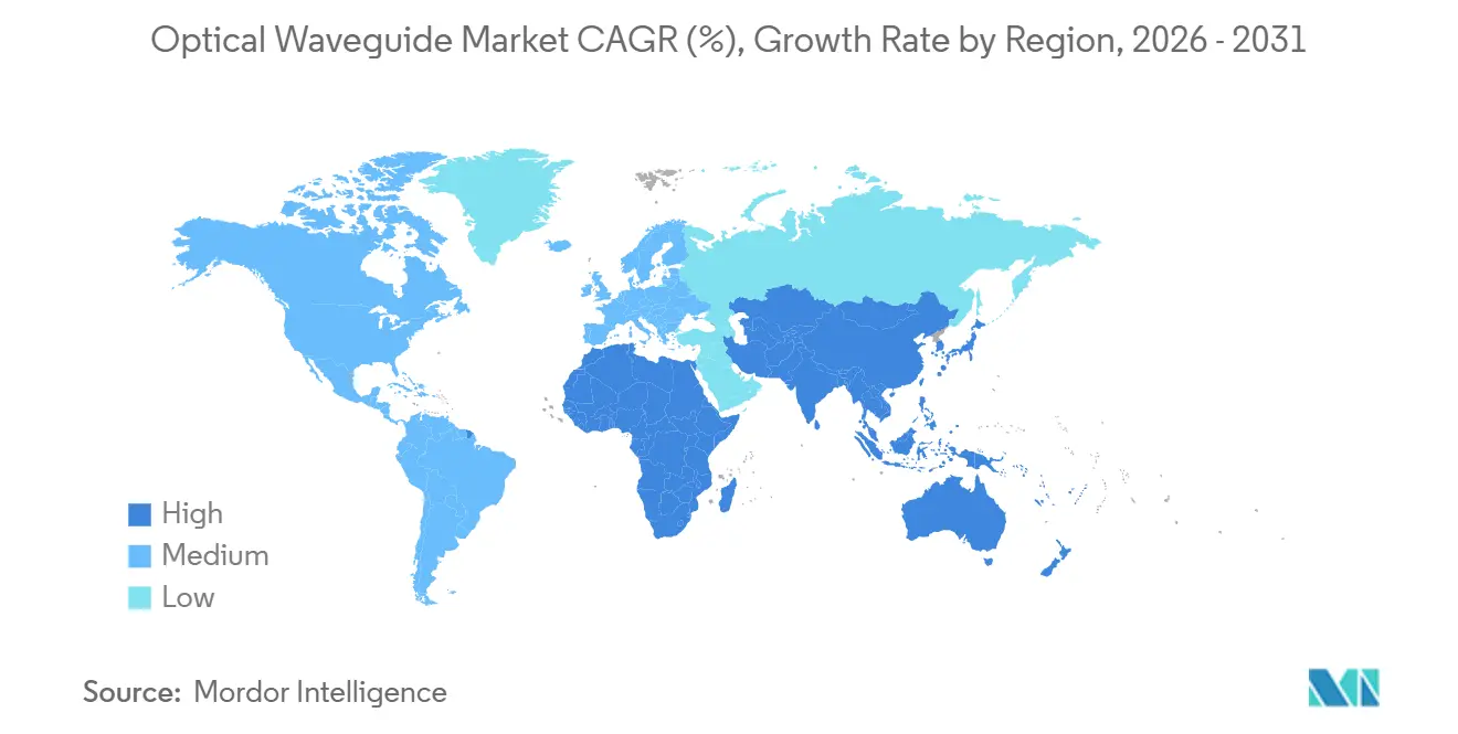
- By geography, Asia-Pacific commanded 32.63% of the optical waveguide market share in 2025, and is expanding at a 7.25% CAGR through 2031
Note: Market size and forecast figures in this report are generated using Mordor Intelligence’s proprietary estimation framework, updated with the latest available data and insights as of January 2026.
Global Optical Waveguide Market Trends and Insights
Drivers Impact Analysis*
| Driver | (~) % Impact on CAGR Forecast | Geographic Relevance | Impact Timeline |
|---|---|---|---|
| Surge in silicon-photonics datacenter deployments | +1.8% | Global, with concentration in North America and Asia-Pacific hyperscale clusters | Medium term (2-4 years) |
| 5G and fiber-to-the-home roll-outs demanding low-loss integrated waveguides | +1.5% | Asia-Pacific core, spill-over to Middle East and South America | Medium term (2-4 years) |
| Rapid adoption of polymer waveguides in co-packaged optics modules | +1.2% | North America and Europe, early adoption in Asia-Pacific fabs | Short term (≤ 2 years) |
| Mid-infrared sensing driving fluoride-glass waveguide demand | +0.7% | Europe and North America for industrial monitoring, Asia-Pacific for environmental compliance | Long term (≥ 4 years) |
| Defense LiDAR programs leveraging low-size-weight-and-power photonic integrated circuit waveguides | +0.6% | North America and Europe defense contractors, selective Asia-Pacific programs | Long term (≥ 4 years) |
| Government chip-on-board photonics funding | +0.5% | United States (CHIPS Act), European Union (Photonics21), China (National IC Fund), Japan (METI) | Medium term (2-4 years) |
| Source: Mordor Intelligence | |||
Surge in Silicon-Photonics Datacenter Deployments
Hyperscale operators are shifting from discrete optics to co-packaged architectures that situate silicon-nitride or silicon-rich-oxide waveguides beside 5-nanometer switch cores. Multi-year purchase commitments from tier-one cloud providers now underwrite entire foundry runs, accelerating design cycles and standardizing electro-optical interfaces across switch silicon. Volume production that began in 2026 collapses qualification timelines because the photonics die and ASIC share a single test flow, boosting the optical waveguide market penetration in core switches and line cards. Power envelopes below 5 watts per 1.6 terabit lane make optical links attractive against retimer-heavy electrical backplanes, especially as rack densities move past 30 kilowatts. Combined, these forces elevate attach rates in datacenter capital-expenditure budgets and underpin the most influential demand inflection for the optical waveguide market this decade.
5G and Fiber-to-the-Home Roll-Outs Demanding Low-Loss Integrated Waveguides
Carrier-grade passive optical networks split a single feeder into 32 to 64 drops, mandating planar-lightwave-circuit splitters with sub-0.3 decibel insertion loss. National broadband programs underway across Asia-Pacific, the Middle East, and parts of South America upgrade copper last-mile links to fiber, guaranteeing multi-year volume visibility for low-loss silica and glass waveguides. Equipment vendors integrate waveguide-based wavelength-division multiplexers directly into optical line terminals, shrinking the rack footprint and trimming power draw by eliminating separate splitter trays. Urban build-outs are mirrored by rural subsidies that fund hardened outdoor enclosures where polymer waveguides tolerate extreme temperature swings better than silica, further broadening the materials mix. Deployment velocity keeps factory utilization high and offsets cyclical pauses in datacenter spending, stabilizing baseline growth for the optical waveguide market.
Rapid Adoption of Polymer Waveguides in Co-Packaged Optics Modules
Polymer waveguides are processed at temperatures below 200 degrees Celsius, aligning with organic-substrate reflow temperatures and avoiding coefficient-of-thermal-expansion mismatches that warp silicon-on-insulator stacks.[2]IEEE Xplore Authors, “Polymer Waveguides for Co-Packaged Optics,” ieee.org Propagation losses near 0.1 decibel per centimeter, once relegated to academic proofs, now meet hyperscaler loss budgets after 2025 material refinements. Shorter cycle times, days instead of weeks, enable design iterations that match the cadence of electronic chiplets, allowing photonic and logic teams to share agile methodologies. High refractive-index contrast enables 200-micrometer bend radii, packing hundreds of optical traces under a single heat spreader and advancing chiplet-to-chiplet communication fabrics. As co-packaged optics migrates from switches to AI accelerators, the optical waveguide market benefits from polymer’s speed-to-scale and cost-retention advantages.
Mid-Infrared Sensing Driving Fluoride-Glass Waveguide Demand
Industrial emissions monitoring and environmental compliance regulations specify mid-infrared spectroscopy, a window where silica absorbs strongly. Fluoride-glass waveguides transmit wavelengths of 2 to 5 micrometers with losses below 1 decibel per meter, enabling distributed sensors that detect methane or volatile organic compounds in pipelines and chemical plants. European mandates for continuous emissions scanning and North American methane-fee frameworks are accelerating commercial orders for fluoride-glass components beyond the traditional telecom base. Recent demonstrations of high-power fluoride-glass lasers have validated reliability at field temperatures from −40 to +85 degrees Celsius, satisfying oil-and-gas ruggedization standards. Although a niche in revenue terms, unit prices are several times higher than those of telecom splitters, raising value density and diversifying the optical waveguide market revenue pool.
Restraints Impact Analysis*
| Restraint | (~) % Impact on CAGR Forecast | Geographic Relevance | Impact Timeline |
|---|---|---|---|
| High capital intensity of lithographic fabs for sub-micron waveguides | -1.1% | Global, acute in regions lacking established semiconductor ecosystems | Long term (≥ 4 years) |
| Complex coupling losses versus optical fibers | -0.9% | Global, particularly impacting short-reach datacenter and telecom applications | Medium term (2-4 years) |
| Material thermo-optic instability in extreme environments | -0.5% | Aerospace, defense, and automotive sectors in North America and Europe | Medium term (2-4 years) |
| Intellectual property bottlenecks around proprietary planar lightwave circuit and arrayed waveguide grating designs | -0.4% | Asia-Pacific manufacturers seeking to enter North American and European markets | Short term (≤ 2 years) |
| Source: Mordor Intelligence | |||
High Capital Intensity of Lithographic Fabs for Sub-Micron Waveguides
Extreme-ultraviolet (193-nanometer) immersion tools cost upward of USD 150 million, and only a dozen global customers operate the latest steppers. Photonic designers therefore compete with higher-margin logic and memory for wafer starts, stretching prototype lead times to months. Shared foundry models help amortize costs but still impose minimum orders that early-stage firms cannot meet, narrowing the supplier base. Nations without semiconductor ecosystems face additional hurdles in securing utilities, cleanroom talent, and equipment import licenses, delaying waveguide capacity expansion. Unless dedicated photonic fabs achieve sustained utilization or lower-cost maskless lithography matures, capital intensity will remain the chief brake on the growth of the optical waveguide market.
Complex Coupling Losses Versus Optical Fibers
Mode-field mismatch between 9-micrometer fiber cores and sub-micron silicon waveguides introduces 1 to 3 decibels of insertion loss per interface, eroding power budgets and requiring additional gain stages. Grating couplers reduce assembly tolerances but incur polarization sensitivity, while edge-coupled facets require sub-nanometer surface polish, which elevates die cost. Automated 3D-printed lenses cut manual alignment time, yet each channel adds material expense that accumulates across 32-lane modules. Yield penalties multiply when multiple optical dies populate a single package, challenging wafer-level test coverage and stressing supply plans. Until average losses fall below 0.3 decibels per transition, the optical waveguide market penetration into legacy fiber plants and cost-sensitive edge nodes will stay constrained.
*Our forecasts treat driver/restraint impacts as directional, not additive. The impact forecasts reflect baseline growth, mix effects, and variable interactions.
Segment Analysis
By Waveguide Type: Planar Strength Meets Photonic-Crystal Momentum
Planar designs captured 37.29% of revenue in 2025, anchoring telecom passive components through maturity, low cost, and insertion losses below 0.2 decibels per centimeter. Photonic-crystal implementations, although starting from a small base, are forecast to grow at 7.11% annually as defense contractors embed air-core bandgap structures into compact LiDAR, widening the optical waveguide market addressable sensor field. Channel, fiber, and ridge variants serve optical backplanes and modulators that trade ultra-low loss for tighter bends, while the photonic-crystal class sacrifices fabrication simplicity for unmatched confinement. Together, these form factors illustrate how the optical waveguide market balances legacy volume with frontier performance needs.
Volume advantages accrue to planar silica, where wafer-scale dicing yields thousands of identical splitters that underpin passive optical networks worldwide. Fiber waveguides, although technologically static, remain irreplaceable wherever splice compatibility outweighs integration density. Ridge geometries occupy the performance midpoint and dominate silicon photonics modulators shipped in 400-gigabit and 800-gigabit pluggable transceivers. Photonic-crystal lines are incubated in defense labs and now migrate to commercial drones, spotlighting a premium niche whose influence on the broader optical waveguide market will expand alongside advanced sensing budgets.


By Material: Silica Entrenched as Polymers and Semiconductors Surge
Glass and silica platforms held 48.91% of 2025 revenue, underscoring their 30-year incumbency and unrivaled loss floor in passive splitters, an advantage that stabilizes half of the optical waveguide market size. Polymer lines, on a 6.72% CAGR path, benefit from low-temperature deposition that pairs seamlessly with package substrates, enabling faster prototyping and lower capex per layer. Semiconductor materials, silicon, silicon nitride, indium phosphide, and gallium arsenide, provide active modulation, detection, and amplification, prerequisites for co-packaged AI accelerators and coherent telecom links.
Silica’s dominance persists in fiber-to-the-home gear, yet data-center silicon-nitride circuits already integrate drivers, photodiodes, and waveguides on one die, cutting board real estate by double digits. Lithium niobate thin films re-enter volume production with CHIPS Act funding, offering electro-optic coefficients an order of magnitude above those of silicon while keeping propagation loss below 0.1 decibel per centimeter.[3]GAO, “CHIPS Act Implementation Review GAO-25-105678,” gao.gov The diverging performance envelopes enable material coexistence and broaden the market's application reach, a duality that enhances the optical waveguide market's resilience against single-material supply disruptions.
By Mode Structure: Single-Mode Core, Multi-Mode Upside
Single-mode architectures contributed 61.19% of 2025 deployments, leveraging dispersion-free propagation indispensable for coherent long-haul systems. Multi-mode designs, gaining at a 6.85% CAGR, deliver relaxed alignment and cost efficiency in short-reach datacenter interposers, expanding the optical waveguide market beyond telecom trenches. As clock rates exceed 100 gigabaud, single-mode remains the only option for error-free transmission over kilometers, but multi-mode’s wider cores and graded-index profiles now push one-kilometer reach, opening brownfield switch-to-server upgrades without tight tolerance demands.
Fabricators balance these traits by mixing single-mode paths for clock distribution and multi-mode traces for bulk data, demonstrating hybrid photonic packaging flexibility. Bend-loss ceilings differ; multi-mode channels sustain 10 micrometer radii that single-mode cannot match, enabling dense routing under chip heat spreaders. Such complementary roles reinforce the market's application diversity, which fortifies the outlook for the optical waveguide market.
By Application: Telecom Foundation, AR/VR Acceleration
Telecommunications and datacom retained a 43.43% share in 2025, underwriting base volumes through passive optical network rollouts and 800-gigabit coherent upgrades. Consumer electronics and AR/VR, however, chart the fastest expansion at 6.94% CAGR, with holographic combiners and diffractive displays injecting new unit demand. Industrial sensing, medical diagnostics, and defense LiDAR layer auxiliary revenue streams that buffer the optical waveguide market against swings in carrier capital expenditure.
Telecom growth moderates as fiber access saturates mature economies, yet co-packaged optics refresh cycles inject a second upgrade phase within the same racks. AR/VR’s upside remains contingent on stylish, lightweight glasses overcoming yield and cost hurdles, yet every prototype iteration consumes pilot lots of polymer and diffractive waveguides. Environmental regulation and point-of-care diagnostics ensure recurring shipments in sensing and medical verticals, knitting a balanced application portfolio that underlies sustained expansion of the optical waveguide market.
By Fabrication Process: Lithography Scale, Laser Agility
Lithographic etching secured 52.15% of 2025 revenue, translating semiconductor fab discipline into photonics with overlay accuracy below 5 nanometers that dense arrayed waveguide gratings demand. Ultrafast laser inscription, poised for a 7.06% CAGR, fabricates three-dimensional paths inside bulk glass without masks, shortening prototype turnaround and enabling quantum photonic layouts that planar tracks cannot emulate. Ion-exchange and sol-gel routes serve specialty optics where sub-micron resolution is secondary to cost and volume flexibility, keeping small-batch innovators active in the optical waveguide market.
Economies of scale favor lithography whenever volumes crest thousands of wafers, yet femtosecond-laser writing’s serial process sidesteps USD 500,000 mask sets, appealing to academia and defense labs. Shared fabs offering multi-project wafers democratize access, but maskless alternatives garner traction in regions lacking advanced lithography. This dual-track evolution enables the optical waveguide market to accommodate both mass-produced datacenter gear and bespoke photonic circuits for emerging quantum and sensing use cases.
Geography Analysis
Asia-Pacific contributed 32.63% of global revenue in 2025 and is expanding at a 7.25% CAGR, the fastest regional pace in the optical waveguide market. China, Japan, and South Korea collectively invest more than USD 21 billion in silicon photonics capacity, funding 300-millimeter fabs that co-package waveguides with memory and logic. National broadband policies extend fiber-to-the-home beyond megacities, securing large passive component orders that lock in fab utilization.
North America remains critical due to CHIPS Act incentives exceeding USD 30 billion and its outsized share of hyperscale data centers. Pilot lines for indium-phosphide and lithium-niobate modulators progress, but construction lead times prolong first-silicon into late 2027, tempering near-term shipment growth. Europe targets a USD 56.5 billion turnover by 2035 under Photonics21, yet fragmented national programs delay the development of unified supply chains, a gap that Asia-Pacific bridges through centrally planned megafabs.[4]Photonics21, “Strategic Roadmap 2025,” photonics21.org
South America scales fiber backbones across Brazil and Argentina, importing planar-lightwave circuits from Asia-Pacific to sidestep local capex. Middle Eastern smart-city ventures such as NEOM specify 10 terabit backbones populated with waveguide-based multiplexers, although project slippage past 2030 blunts immediate impact. Africa’s fiber penetration below 5% signals long-term potential but near-term demand headwinds. Overall, regional dynamics preserve Asia-Pacific’s lead while keeping multilateral funding momentum intact for the optical waveguide market.

Competitive Landscape
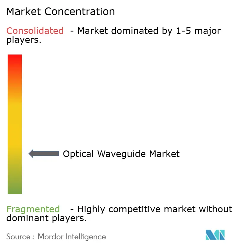
Revenue concentration is moderate: the top five suppliers control about 40% to 45% share. Vertically integrated fiber incumbents, Corning, Sumitomo Electric, Fujikura, Prysmian, and YOFC, bundle passive splitters with connectors and fusion splicers, shielding share in legacy telecom deployments. Yet co-packaged optics disrupts this moat because fabless photonic designers license intellectual property to open-access foundries, bypassing discrete module vendors and shortening design loops to months.
Ayar Labs, Lightmatter, and other chiplet specialists leverage GlobalFoundries and TSMC multi-project wafers to land Meta and Microsoft reference designs, proving fab-light models viable.[5]Ayar Labs, “TeraPHY Chiplet Press Release 2025,” ayarlabs.com Mid-infrared sensing carves a premium niche for fluoride-glass suppliers whose unit prices eclipse telecom averages, while ultrafast laser inscription vendors unlock 3D waveguide routing for quantum photonics. Patent filings show divergent bets: NTT and Furukawa Electric pursue athermal arrayed waveguide grating solutions, whereas Lightwave Logic doubles down on electro-optic polymers that promise sub-one-volt modulators, pending proof of material lifetime. Equipment vendor ASML anchors capital barriers; extreme-ultraviolet steppers above the USD 200 million threshold, new entrants, and consolidation of high-volume photonic runs at a handful of semiconductor mega-fabs.
Strategic moves continue. NVIDIA’s USD 4 billion, multi-year allocation locks in supply from Lumentum and Coherent, while Coherent’s own USD 112 million federally backed expansion strengthens thin-film lithium-niobate throughput. Joint programs such as LIGENTEC and X-FAB’s polymer-waveguide pilot halve flow time and open polymer platforms to a broader design community, injecting agility into a market historically defined by glass and silica incumbents. The competitive frontier, therefore, pivots less on unit share and more on materials breakthroughs, access to fabrication, and package-level integration roadmaps that will set the trajectory for the optical waveguide market over the next decade.
Optical Waveguide Industry Leaders
Corning Incorporated
Sumitomo Electric Industries, Ltd.
Fujikura Ltd.
Prysmian S.p.A.
Yangtze Optical Fibre and Cable Joint Stock Limited Company
- *Disclaimer: Major Players sorted in no particular order

Recent Industry Developments
- March 2026: STMicroelectronics began commercial shipments of 1.6 terabit-per-second co-packaged optics modules that eliminate the need for external fiber-optic transceivers in datacenter switches.
- March 2026: NVIDIA committed USD 4 billion to Lumentum and Coherent for waveguide-integrated chiplets powering hyperscale AI clusters.
- February 2026: TSMC announced volume production of its COUPE co-packaged optics platform, integrating silicon-nitride waveguides with high-bandwidth memory, delivering 10 terabit aggregate bandwidth per package.
- January 2025: Infinera received a USD 93 million CHIPS Act incentive to expand indium phosphide coherent transceiver production in California.


Global Optical Waveguide Market Report Scope
The Optical Waveguide Market Report is Segmented by Waveguide Type (Planar, Channel/Strip, Fiber, Ridge/Rib, Photonic-Crystal), Material (Glass/Silica, Polymer, Semiconductor, Lithium-Niobate and Other Crystalline), Mode Structure (Single-Mode, Multi-Mode), Application (Telecommunications and Datacom, Industrial and Environmental Sensing, Medical and Life Sciences, Consumer Electronics and AR/VR, Defense and Aerospace), Fabrication Process (Lithographic Etching, Ultrafast Laser Inscription, Ion-Exchange, Sol-Gel/CVD), and Geography (North America, South America, Europe, Asia-Pacific, Middle East, Africa). The Market Forecasts are Provided in Terms of Value (USD).
| Planar Waveguides |
| Channel / Strip Waveguides |
| Fiber Waveguides |
| Ridge / Rib Waveguides |
| Photonic-Crystal Waveguides |
| Glass / Silica |
| Polymer |
| Semiconductor (Si, SiN, InP, GaAs) |
| Lithium-Niobate and Other Crystalline |
| Single-Mode |
| Multi-Mode |
| Telecommunications and Datacom |
| Industrial and Environmental Sensing |
| Medical and Life Sciences |
| Consumer Electronics and AR/VR |
| Defense and Aerospace |
| Lithographic Etching |
| Ultrafast Laser Inscription |
| Ion-Exchange |
| Sol-Gel / CVD |
| North America | United States |
| Canada | |
| Mexico | |
| South America | Brazil |
| Argentina | |
| Rest of South America | |
| Europe | Germany |
| United Kingdom | |
| France | |
| Russia | |
| Rest of Europe | |
| Asia-Pacific | China |
| Japan | |
| India | |
| South Korea | |
| Australia | |
| Rest of Asia-Pacific | |
| Middle East | Saudi Arabia |
| United Arab Emirates | |
| Rest of Middle East | |
| Africa | South Africa |
| Egypt | |
| Rest of Africa |
| By Waveguide Type | Planar Waveguides | |
| Channel / Strip Waveguides | ||
| Fiber Waveguides | ||
| Ridge / Rib Waveguides | ||
| Photonic-Crystal Waveguides | ||
| By Material | Glass / Silica | |
| Polymer | ||
| Semiconductor (Si, SiN, InP, GaAs) | ||
| Lithium-Niobate and Other Crystalline | ||
| By Mode Structure | Single-Mode | |
| Multi-Mode | ||
| By Application | Telecommunications and Datacom | |
| Industrial and Environmental Sensing | ||
| Medical and Life Sciences | ||
| Consumer Electronics and AR/VR | ||
| Defense and Aerospace | ||
| By Fabrication Process | Lithographic Etching | |
| Ultrafast Laser Inscription | ||
| Ion-Exchange | ||
| Sol-Gel / CVD | ||
| By Geography | North America | United States |
| Canada | ||
| Mexico | ||
| South America | Brazil | |
| Argentina | ||
| Rest of South America | ||
| Europe | Germany | |
| United Kingdom | ||
| France | ||
| Russia | ||
| Rest of Europe | ||
| Asia-Pacific | China | |
| Japan | ||
| India | ||
| South Korea | ||
| Australia | ||
| Rest of Asia-Pacific | ||
| Middle East | Saudi Arabia | |
| United Arab Emirates | ||
| Rest of Middle East | ||
| Africa | South Africa | |
| Egypt | ||
| Rest of Africa | ||


Key Questions Answered in the Report
What is the projected value of the optical waveguide market by 2031?
The optical waveguide market size is expected to reach USD 11.68 billion by 2031 at a 6.22% CAGR.
Which region is growing fastest in optical waveguides?
Asia-Pacific leads growth with a 7.25% CAGR, supported by large semiconductor and broadband investments.
Why are polymer waveguides gaining traction?
They process below 200 °C, cut cycle times in half and meet datacenter loss budgets, making them ideal for co-packaged optics.
What is the main restraint limiting wider adoption?
High capital intensity of extreme-ultraviolet lithography keeps new fabs scarce and raises entry barriers.
How do co-packaged optics influence demand?
By integrating waveguides next to switch ASICs, co-packaged optics remove pluggable modules, driving a step-change in embedded waveguide volumes.
Page last updated on:


