
Semiconductor Laser Market Size and Share
Market Overview
| Study Period | 2020 - 2031 |
|---|---|
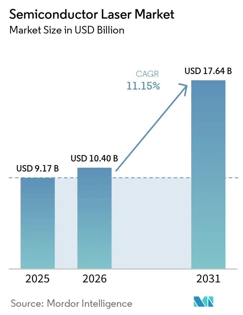
| Market Size (2026) | USD 10.40 Billion |
| Market Size (2031) | USD 17.64 Billion |
| Growth Rate (2026 - 2031) | 11.15 % |
| Fastest Growing Market | Middle East |
| Largest Market | Asia Pacific |
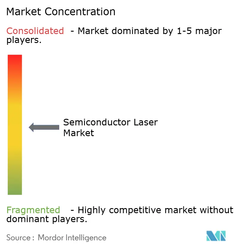
| Market Concentration | Medium |
Major Players *Disclaimer: Major Players sorted in no particular order Image © Mordor Intelligence. Reuse requires attribution under CC BY 4.0. | |
Semiconductor Laser Market Analysis by Mordor Intelligence
The Semiconductor Laser Market size is expected to increase from USD 9.17 billion in 2025 to USD 10.40 billion in 2026 and reach USD 17.64 billion by 2031, growing at a CAGR of 11.15% over 2026-2031. Persistent upgrades to data-center bandwidth, rising automotive safety mandates, and wider consumer adoption of 3D sensing are supporting double-digit revenue expansion, even as compound-semiconductor wafer shortages and thermal-management limits at higher power densities moderate the growth trajectory. Vertical-cavity surface-emitting lasers (VCSELs) held the leading 37.8% share in 2025, propelled by smartphone facial authentication and time-of-flight modules, while quantum cascade lasers (QCLs) are forecast to grow the fastest at a 16.3% CAGR thanks to stronger budgets for industrial gas-sensing and defense chemical-detection systems. Communication applications represented the largest 34.12% revenue slide in 2025, yet automotive end-use is advancing the quickest at 13.2% CAGR as Euro NCAP’s 2025 rules make LiDAR-enabled autonomous emergency braking compulsory. Infrared wavelengths dominated with a 42.5% share, but ultraviolet variants are accelerating at 14.8% CAGR, driven by the demand for extreme-ultraviolet (EUV) lithography tools and medical UV-curable additive manufacturing. Asia-Pacific contributed 48.2% of 2025 revenue, buoyed by China’s gallium-arsenide substrate capacity and Japan’s legacy edge-emitting production; the Middle East is the fastest-growing sub-region at 12.9% CAGR as Saudi Vision 2030 and UAE smart-city programs scale photonics investment.
Key Report Takeaways
- By laser type, VCSELs captured a 37.8% market share of the semiconductor laser market in 2025, while QCLs are set to log the steepest 16.3% CAGR through 2031.
- By application, communication retained the top 34.12% share in 2025, whereas the automotive sector is expanding fastest at a 13.2% CAGR, thanks to LiDAR integration.
- By wavelength, infrared accounted for a dominant 42.5% share in 2025; ultraviolet is forecast to rise at a 14.8% CAGR to 2031.
- By power output, the 100 mW-to-1 W bracket held 46.6% of the semiconductor laser market share in 2025, while devices exceeding 5 W are expected to grow at a 15.7% CAGR over the forecast period.
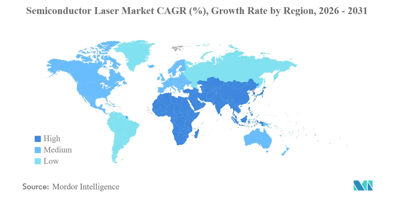
- By geography, Asia Pacific held 48.2% was the largest semiconductor laser market in 2025, while Middle-east and Africa is expected to lead 12.9% CAGR growth through 2031 as manufacturing capacity and data-center-driven photonics demand accelerate.
Note: Market size and forecast figures in this report are generated using Mordor Intelligence’s proprietary estimation framework, updated with the latest available data and insights as of January 2026.
Market Trends and Insights
Drivers Impact Analysis of Semiconductor Laser Market*
| Driver | (~) % Impact on CAGR Forecast | Geographic Relevance | Impact Timeline |
|---|---|---|---|
| Rapid Expansion of 3D Sensing in Consumer Electronics | +3.2% | Global, with concentration in Asia-Pacific manufacturing hubs and North America design centers | Short term (≤ 2 years) |
| Emerging Demand from Silicon Photonics Interconnects | +2.8% | North America and Asia-Pacific data-center corridors, spillover to Europe | Medium term (2-4 years) |
| Proliferation of Semiconductor Laser Applications | +2.5% | Global | Medium term (2-4 years) |
| Government-Backed Photonics Manufacturing Initiatives | +1.9% | United States, European Union, China, Japan | Long term (≥ 4 years) |
| Growth in Fiber Laser Adoption | +1.5% | Global, with emphasis on Asia-Pacific and European industrial manufacturing regions | Medium term (2-4 years) |
| Preference for Semiconductor Lasers over Other Light Sources | +1.2% | Global | Medium term (2-4 years) |
| Source: Mordor Intelligence | |||
Rapid Expansion of 3D Sensing in Consumer Electronics
VCSEL array shipments for time-of-flight and structured-light modules surged as smartphone vendors broadened facial authentication and augmented-reality features, with wall-plug efficiencies topping 45% and reliable operation up to 150 °C without active cooling [1]Source: Nature Photonics, “VCSEL Technology Advances for 3D Sensing Applications,” nature.com . Sony leveraged its back-illuminated sensor expertise to co-package VCSEL dies and CMOS detectors, reducing module footprints by 30% and lowering unit costs to below USD 2 in high-volume orders. Android flagship adoption increased from 18% in 2023 to an estimated 42% in 2025, as manufacturers sought to secure payments and differentiate their products. Euro NCAP cabin-monitoring rules triggered dual-zone VCSEL illuminators that withstand temperatures ranging from -40 °C to +85 °C, thereby tightening epitaxial uniformity requirements. Wearables add another growth vector, with smart glasses and health monitors forecast to exceed 50 million units annually by 2028 as sub-5 mm VCSEL modules enable gesture recognition and non-contact heart-rate sensing.
Emerging Demand from Silicon Photonics Interconnects
Hyperscale operators transitioned from 400G to 800G Ethernet between 2024 and 2025, integrating heterogeneously bonded III-V lasers on silicon to achieve sub-3W lane power and coupling losses of below 0.5 dB. Co-packaged optics place laser arrays directly on switch ASICs, eliminating SerDes bottlenecks and cutting latency by 40 ns, an edge prized for AI training clusters. DARPA committed USD 203 million in 2025 to lift heterogeneous integration yields toward 95%. The current wall-plug efficiency hovers near 10%, falling short of the 20% thermal envelope for air-cooled racks, which has spurred research on quantum-dot gain media and photonic-crystal cavities aimed at achieving 15% by 2027. Kerr frequency combs are displacing discrete arrays, providing 80 channels from one micro-resonator and reducing transceiver bills of materials by 35% in metro networks.
Proliferation of Semiconductor Laser Applications
Automotive body-in-white welding now utilizes 8 kW semiconductor-pumped fiber lasers, whose 100 µm beams enable single-pass welds on 3 mm aluminum without preheating. Medical manufacturers utilize 355 nm UV lasers for sub-10 µm stent cutting, with heat-affected zones of less than 5 µm. Military rangefinders moved to compact semiconductor lasers, slashing system weight by 40% and extending battery life to 72 hours, aligning with NATO soldier-modernization goals. Quantum cascade networks detect methane leaks with a sensitivity of sub-ppb, fulfilling the U.S. EPA's 2024 rule for upstream oil and gas operators. Additive manufacturing leverages 365 nm and 405 nm diodes to cure layers in under 2 seconds, enabling biocompatible implants with <1 µm surface roughness.
Government-Backed Photonics Manufacturing Initiatives
The CHIPS and Science Act earmarks USD 52.7 billion for semiconductors, including USD 300 million for advanced packaging that specifically names photonics. DARPA’s LUMOS program invests USD 10 million to demonstrate monolithic distributed-feedback lasers on silicon. The EU’s Horizon initiative commits EUR 25 million to integrated photonics, targeting <1 dB coupling loss and 200 mm wafer scaling. China’s Phase III Big Fund reserves CNY 200 billion (≈ USD 28 billion) for gallium-nitride and indium-phosphide capacity, with provincial subsidies covering 30% of capex. Japan’s METI launched a JPY 50 billion (~ USD 340 million) photonics program in 2025 to build 6-inch gallium-arsenide pilot lines and cut costs by 20% through automation.
Restraints Impact Analysis of Semiconductor Laser Market*
| Restraint | (~) % Impact on CAGR Forecast | Geographic Relevance | Impact Timeline |
|---|---|---|---|
| Supply Chain Volatility of Compound Semiconductor Wafers | -1.8% | Global, with acute pressure in North America and Europe, dependent on the Asia-Pacific substrate supply | Short term (≤ 2 years) |
| Thermal Management Challenges at High Power Outputs | -1.3% | Global, most pronounced in industrial and automotive high-power applications | Medium term (2-4 years) |
| Stringent Export Controls on Advanced Photonics | -0.9% | Global, particularly affecting trade between the United States, the European Union, and China | Medium term (2-4 years) |
| Difficulties Regarding Reliability and Testing | -0.7% | Global, with heightened impact in automotive and medical device qualification cycles | Medium term (2-4 years) |
| Source: Mordor Intelligence | |||
Supply Chain Volatility of Compound Semiconductor Wafers
Four suppliers control 78% of global gallium-arsenide wafer capacity, leaving the semiconductor laser market exposed to sudden demand swings. China’s August 2023 curbs on gallium and germanium stretched 6-inch substrate lead times from 12 to 26 weeks and pushed spot prices 40% higher by early 2024. Hyperscale buyers locked long-term indium-phosphide contracts, crowding smaller diode makers toward less flexible gallium-arsenide alternatives. Dual-sourcing requires 18–24 months of AEC-Q100 and Telcordia GR-468-CORE testing, which delays diversification. Scaling from 4- to 6-inch wafers remains capital-intensive; a single MOCVD reactor costs USD 4 million and needs 95% utilization for a 5-year payback.
Thermal Management Challenges at High Power Outputs
Junction temperatures above 100 °C in ≥5 W lasers shift wavelengths by 0.3 nm/°C and reduce quantum efficiency by 15% compared to 25 °C baselines. Thermoelectric coolers add USD 8–12 per module and 3–5 W of parasitic power, tightening system-level efficiency. Achieving <2 K/W thermal resistance in <10 mm² packages needs gold-tin or sintered-silver attach, increasing assembly cost by 25% and lowering yields. Catastrophic optical damage risk climbs when local heating exceeds 150 °C, shortening mean time between failures from 100,000 hours at 25 °C to <20,000 hours at 85 °C. Liquid cooling works in labs but is impractical for consumer and automotive gear, forcing designers to trade output power against reliability and size.
*Our forecasts treat driver/restraint impacts as directional, not additive. The impact forecasts reflect baseline growth, mix effects, and variable interactions.
Semiconductor Laser Market Segment Analysis
By Wavelength:
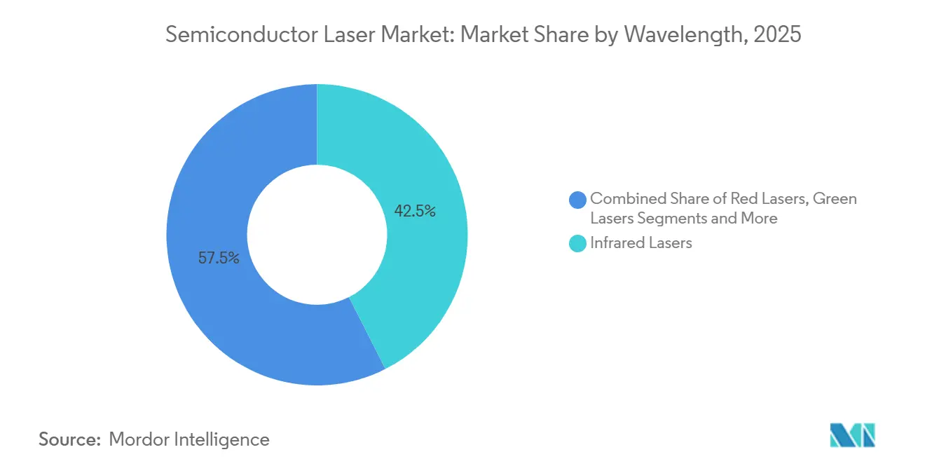
Infrared Scale Anchors Growth While Ultraviolet AcceleratesInfrared lasers accounted for 42.5% of 2025 revenue, underpinning the semiconductor laser market through 850 nm and 1,550 nm devices that dominate consumer 3D sensing and long-haul fiber links [2]Source: Optica Publishing Group, “Miniaturized VCSEL Modules,” opg.optica.org. Ultraviolet variants, although smaller in absolute dollars, will climb at a 14.8% CAGR to 2031 on EUV lithography shipments and medical UV-curable prototyping, pointing to a rising semiconductor laser market size contribution from advanced manufacturing tools. The rising demand for semiconductor chips throughout various end-user sectors creates a favorable market setting for the semiconductor laser equipment market's growth.
VCSEL-based infrared modules deliver circular beams that simplify coupling, while QCL-based mid-infrared sources provide tunability for gas sensing. Ultraviolet penetration remains cost-sensitive but emerging 266 nm diodes promise higher yields and longer lifetimes. Regulatory IEC 60825 Class 3B and Class 4 limits demand sophisticated interlocks above 5 mW, influencing design budgets and time to market. As advanced logic nodes migrate below 3 nm, lithography tool vendors will propel ultraviolet demand, reinforcing its double-digit climb within the semiconductor laser market.



By Laser Type:
VCSEL Leadership Faces Quantum Cascade MomentumVCSELs captured a 37.8% share, thanks to wafer-scale testing that reduces die cost below USD 0.50, thereby safeguarding their leadership in the semiconductor laser market. QCLs, however, are racing ahead at a 16.3% CAGR through 2031, as mid-infrared spectroscopy gains regulatory tailwinds, suggesting a growing impact on the semiconductor laser market size from environmental and defense programs.
Edge-emitting bars retain relevance for multi-kilowatt industrial cutting, yet their 6% CAGR lags. Fiber lasers, although technically outside the pure semiconductor classification, depend on diode pumping and maintain a 9% trajectory. Narrow-linewidth external-cavity diodes fill metrology niches requiring <1 MHz linewidth. Over the forecast period, design wins in automotive LiDAR and gas monitoring will help QCLs erode VCSEL dominance, diversifying revenue streams within the semiconductor laser market.
By Application:
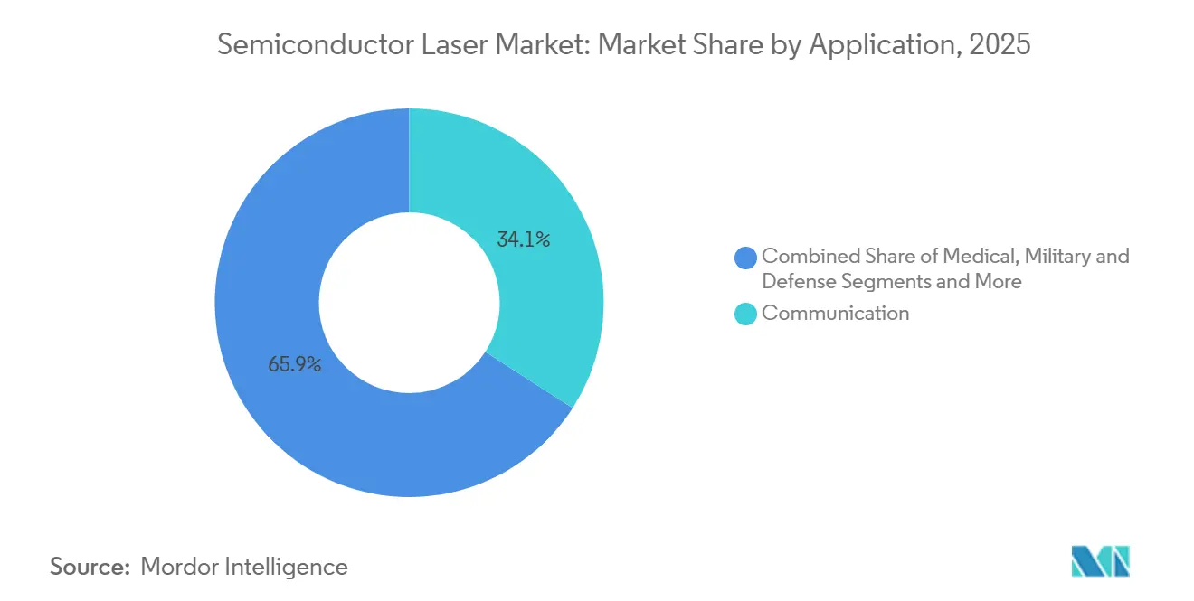
Communication Dominance Meets Automotive UpswingCommunication retained the largest 34.12% revenue slice in 2025, leveraging VCSEL-based 100 Gbit short-reach links and 1,550 nm coherent modules for metro spans. Automotive, however, is tracking a 13.2% CAGR, and its expanding sensor suite is set to lift the semiconductor laser market size in safety-critical systems through 2031.
Medical demand advances 8% annually as femtosecond ophthalmic and dermatology systems grow procedure volumes. Military programs sustain a 10% CAGR on airborne rangefinders and directed-energy prototype funding. Industrial automation and instrumentation continue to maintain steady single-digit gains, but LiDAR-driven automotive growth keeps the spotlight on as original-equipment manufacturers secure multi-year contracts.
By Power Output:
Mid-Range Prevalence Yields to High-Power MomentumLasers rated 100 mW–1 W held 46.6% of the semiconductor laser market share in 2025, anchored by consumer biometrics and short-reach optics. Devices above 5 W will surge at a 15.7% CAGR, thanks to sheet-metal cutting migrations and pulsed automotive LiDAR, which will buoy the overall semiconductor laser market size for industrial and mobility users.
Below-100 mW pointers inch ahead at 4% as smartphones displace handheld scanners. The 1 W–5 W bracket maintains an 8% growth rate, catering to surgical tools and projection systems. Higher-power classes face stricter Class 4 compliance, adding cost and engineering complexity, yet their superior throughput justifies the investment in high-volume manufacturing.
Geography Analysis
APAC Semiconductor Laser Market
The Asia-Pacific region generated 48.2% of 2025 revenue, reflecting China’s 60% share of global VCSEL epitaxial wafers and Japan’s 200 million-unit annual diode output. Samsung’s foundry-scale gallium-arsenide services trim wafer costs by 20%, while India’s 25% subsidy attracts new assembly lines. Singapore, Hong Kong, and Tokyo data center expansions, which require 800 Gbit transceivers, are expected to support a 10.8% regional CAGR, keeping the Asia-Pacific region central to the semiconductor laser market.
North America Semiconductor Laser Market
North America remained a significant contributor to 2025 sales, driven by hyperscale cloud consumption, which comprises 40% of global silicon photonics shipments. The CHIPS Act will fund domestic epitaxial wafers; however, new fabs typically require 36 to 48 months to reach volume production. Canada’s CAD 100 million photonics cluster and Mexico’s duty-free equipment imports under USMCA strengthen continental resilience.
EMEA and South America Semiconductor Laser Market
Europe remained a significant revenue contributor, anchored by Germany’s TRUMPF and ams-OSRAM plus Fraunhofer R&D. Horizon funds and UK pilot lines enhance heterogeneous integration, while RoHS and REACH compliance add six-to-twelve-month qualification overhead. The Middle East’s 12.9% CAGR is driven by NEOM’s USD 500 billion investment, which incorporates LiDAR into mobility infrastructure. South America and Africa together supply 6% of the revenue, with Brazil’s.

Regulatory Landscape
Global semiconductor laser shipments are shaped by product-safety classification, end-market equipment safety, and cross-border trade controls on advanced photonics and adjacent semiconductor articles. On laser safety, the IEC 60825 family of guidance continues to anchor design and labeling practices for classed laser products. IEC TS 60825-13:2026 (published February 2026) updates measurement and classification guidance used to support conformity with IEC 60825-1. For device characterization and comparability across suppliers, IEC 60747-5-4:2022+AMD1:2024 standardizes terminology, ratings, and measurement methods for semiconductor lasers, including revisions to radiation-angle definitions and spectral-linewidth reporting.
Medical and high-performance computing policy actions also influence qualification and sourcing strategies. In medical lasers, SIST EN IEC 60601-2-22:2020/A11:2026 (published February 2026) aligns particular safety requirements for medical laser equipment with the EU Medical Device Regulation (EU) 2017/745, tightening documentation and verification expectations for OEMs that integrate semiconductor-laser sources. On trade, US actions in January 2026 introduced 25% ad valorem duties (HTSUS 9903.79.01) on specific semiconductor articles defined by technical performance parameters, while BIS guidance issued in May 2026 reaffirmed enforceable license requirements tied to restricted destinations and entities, adding compliance complexity for globally distributed laser, photonics, and computing supply chains.
Value Chain Analysis
The value chain starts with raw materials and substrates, notably GaAs and InP, then moves into specialty chemicals and gases for epitaxy (MOCVD/MBE) and wafer processing. Die fabrication for edge emitters, VCSELs, and QCLs follows, and downstream packaging and assembly add steps such as facet coating, hermetic or non-hermetic sealing, micro-optics alignment, and thermal solutions (including gold-tin or sintered-silver attach for higher-power devices). After that, lasers are integrated into transceivers, sensor modules, illumination engines, medical and industrial systems, and automotive subsystems. Qualification gates such as Telcordia GR-468-CORE and AEC-Q100 also extend dual-sourcing timelines.
Bottlenecks concentrate upstream and at test and qualification. Indium phosphide capacity and MOCVD tool lead times, together with labor-intensive die cutting and aging tests, constrain high-speed communications supply, while concentrated wafer supply keeps lead times volatile. The chain is also showing stronger vertical integration and lock-in through supply and manufacturing partnerships. Quintessent and IQE (January 2025) announced a quantum dot laser and SOA epitaxial wafer supply chain supported by purchase-order commitments; Sivers Semiconductors collaborated with WIN Semiconductors (March 2025) to scale high-power DFB lasers and arrays for CWDM/DWDM; and Sivers and O-Net Technologies (April 2025) formed an OEM partnership around external laser sources for co-packaged optics in AI data centers. Large buyers and platform owners influence allocation across the chain, and long-term VCSEL supply agreements such as Coherent and Apple (August 2025) tied to Sherman, Texas production pull capacity, packaging, and test resources toward the highest-volume end uses.
Competitive Landscape
The semiconductor laser market is moderately concentrated: the top five suppliers, Coherent, Lumentum, ams-OSRAM, IPG Photonics, and TRUMPF, held about 42% of 2025 revenue [3]Source: Coherent Investor Relations, “Merger Integration Update,” investors.coherent.com. Coherent’s 2022 II-VI merger united gallium-nitride and silicon-carbide capabilities across ultraviolet to 10 µm wavelengths. Lumentum and ams-OSRAM are expanding 6-inch VCSEL lines by 2 million wafers annually, dropping per-die costs by 18% and enabling sub-USD 2 automotive modules.
IPG Photonics maintains its fiber-laser leadership through vertical integration and achieves 30% gross margins, despite Chinese competitors undercutting prices by 25%. TRUMPF collaborates with Fraunhofer to co-develop QCL gas sensors, while Coherent invests USD 150 million in Texas silicon-carbide substrates to localize supply and mitigate Asia risks. Technology differentiation centers on epitaxial design: ams-OSRAM’s VCSEL architecture sustains 50% wall-plug efficiency at 150 °C, extending battery life in mobile devices by 30%.
Regional diversification is intensifying. Lumentum’s Thailand assembly plant hedges geopolitical tension, and Sharp’s 405 nm blue-laser ramp addresses automotive headlamp demand. White-space bets include non-invasive glucose monitoring via 9 µm QCLs, a potential USD 3 billion addressable segment pending clinical validation. Hybrid silicon-III-V co-packaged optics remain years out, but DARPA funding indicates strategic persistence.
Semiconductor Laser Industry Leaders
Coherent Corporation
Nichia Corporation
IPG Photonics Corporation
TRUMPF Group
ams-OSRAM AG
- *Disclaimer: Major Players sorted in no particular order
Semiconductor Laser Market Companies Covered in this Report
- Coherent Corp.
- Sharp Corporation
- Nichia Corporation
- IPG Photonics Corporation
- TT Electronics plc
- Sumitomo Electric Industries Ltd.
- Sheaumann Laser Inc.
- Newport Corporation (MKS Instruments Inc.)
- Panasonic Industry Co. Ltd.
- Rohm Co. Ltd.
- Hamamatsu Photonics K.K.
- Jenoptik AG
- TRUMPF Group
- ams-OSRAM AG
- Lumentum Holdings Inc.
- Broadcom Inc.
- Furukawa Electric Co. Ltd.
- Innolume GmbH
- MACOM Technology Solutions Holdings Inc.
- II-VI Incorporated (now part of Coherent)

Market Opportunities and Future Outlook
AI data-center optics and the shift toward co-packaged optics are creating near-term whitespace in high-speed communications lasers, particularly EML and CW-DFB devices where supply constraints and qualification friction remain visible. In June 2026, TrendForce cited combined monthly production capacity of roughly 50.7 million units for EML and CW-DFB laser diodes to support AI data-center expansion, highlighting how incremental capacity and yield improvements translate into market access for transceiver and co-packaged optics supply chains. Product roadmaps are also moving toward higher per-lane speeds, and new entrants and specialists are using foundry and wafer partnerships to access GaAs/InP process depth, as reflected by PicoJools July 2026 introduction of 200G VCSEL products and its manufacturing partnership with WIN Semiconductors.
Materials and manufacturing sovereignty programs are adding another opportunity layer, centered on substrate and wafer supply resilience for InP and silicon photonics. Sumitomo Electric Industries committed JPY 18 billion (about USD 120 million) in July 2026 to upgrade InP substrate manufacturing at its Itami Works, targeting 3.1x capacity versus fiscal 2024 by fiscal 2028, which supports efforts to relieve upstream constraints. Coherent also signed a July 2026 letter of intent for up to USD 50 million in CHIPS and Science Act funding to expand its 6-inch InP facility in Sherman, Texas, and Tower Semiconductor announced a dual-track Japan expansion for 300 mm silicon photonics and SiGe with USD 1 billion support from the Government of Japan. These actions strengthen opportunities for suppliers that can pair capacity with qualification (Telcordia/automotive) and thermal-management packaging, especially for >5 W classes where reliability and heat extraction remain gating factors.
Recent Industry Developments in Semiconductor Laser Market
- July 2026: Coherent signed a letter of intent for up to USD 50 million in CHIPS and Science Act funding to expand its 6-inch indium phosphide (InP) manufacturing in Sherman, Texas, targeting a larger footprint and higher wafer output. The move tightens domestic supply options for high-speed optical networking and co-packaged optics laser sources and supports broader efforts to reduce bottlenecks in InP-based devices for AI data-center interconnects.
- August 2025: Coherent and Apple expanded their strategic partnership with a new multiyear agreement for VCSEL production at Coherents Sherman, Texas facility. Anchoring volume demand to a named site strengthens capacity utilization and investment confidence for VCSEL manufacturing and packaging, with spillover benefits for cost and process maturity in high-volume 3D sensing and related illumination modules.
- March 2024: Coherent announced 6-inch InP scalable wafer fabrication capabilities at Sherman, Texas and Jarfalla, Sweden to increase capacity for next-generation lasers aimed at AI transceivers and 6G networks. Moving InP production to larger wafers improves economies of scale and yield learning curves, and it also raises competitive pressure on suppliers still constrained by smaller-wafer InP and long qualification cycles.


Semiconductor Laser Market Report Scope and Research Methodology
Market Definition and Coverage
This market covers revenue generated from semiconductor lasers (laser diodes and related semiconductor gain devices) used to produce coherent light for communication, sensing, industrial processing, medical, defense, and automotive uses, across global demand.
Scope exclusions: We exclude non-laser light sources (such as LEDs) and most standalone optical components that do not perform laser emission as their main function.
Segments Covered in This Report
- By Wavelength
- Infrared Lasers
- Red Lasers
- Green Lasers
- Blue Lasers
- Ultraviolet Lasers
- By Laser Type
- Edge-Emitting Lasers (EEL)
- Vertical-Cavity Surface-Emitting Lasers (VCSEL)
- Quantum Cascade Lasers
- Fiber Lasers
- Other Types
- By Application
- Communication
- Medical
- Military and Defense
- Industrial
- Instrumentation and Sensor
- Automotive
- Other Applications
- By Power Output
- Below 100 mW
- 100 mW – 1 W
- 1 W – 5 W
- Above 5 W
- By Geography
- North America
- United States
- Canada
- Mexico
- Europe
- Germany
- United Kingdom
- France
- Italy
- Spain
- Russia
- Rest of Europe
- Asia-Pacific
- China
- Japan
- India
- South Korea
- Australia
- Rest of Asia-Pacific
- Middle East
- Saudi Arabia
- United Arab Emirates
- Turkey
- Rest of Middle East
- Africa
- South Africa
- Nigeria
- Rest of Africa
- South America
- Brazil
- Argentina
- Rest of South America
- North America
Data Sources, Market Sizing, and Validation
Desk Research
Desk work starts by mapping what gets counted as a semiconductor laser shipment and what does not, then aligning those shipment definitions to the application buckets used in industry reporting. We reference public sources such as the US International Trade Commission trade statistics, UN Comtrade, World Semiconductor Trade Statistics releases, IEEE and other peer reviewed photonics journals, and standards or technical notes from bodies such as IEC, to anchor terminology and unit logic.
After that, we build the supporting data layer using company filings, investor decks, press releases, and credible coverage of capacity additions and demand shifts in data communications, sensing, and industrial uses. Paid subscriptions are used selectively for company financials and intelligence, news and financial screening, and patent databases to cross check technology direction and product roadmaps. These named examples are illustrative only, and we also reviewed many other public sources to support data collection, validation, and clarification.
Primary Interviews and Surveys
Primary work is used to pressure test the desk assumptions on shipment mix, average selling price movement, and how demand differs by end use (for example, telecom optics versus automotive sensing). We speak with a spread of manufacturers, component and module participants, distributors, and downstream buyers, and the inputs are checked across APAC, EMEA, and the Americas so regional pricing and supply constraints are not over generalized.
Distribution of primary research fieldwork respondents
| Company type | Respondent position | Region |
|---|---|---|
| Top tier: 37% | CXOs: 13% | APAC: 43% |
| Mid tier: 49% | Functional/Unit leaders: 43% | EMEA: 37% |
| Smaller Players: 14% | Managers: 44% | Americas: 20% |
Market-Sizing & Forecasting
Our model uses a top-down approach in which production, trade flows, and end market adoption signals are reconstructed into a revenue view for semiconductor lasers, and then reconciled against the reported direction of key suppliers and major buying sectors. To keep it practical, the totals are corroborated using selective bottom-up approximations, such as sampled average selling price by laser type multiplied by indicative shipment volumes, then refined through channel checks.
Key inputs include indicators like data center and telecom optics upgrade intensity, 3D sensing penetration in consumer devices, automotive sensing and lighting design wins, industrial laser processing activity, and wavelength and power output mix shifts that change pricing. Since these drivers do not move in the same direction each year, forecasting is done using scenario analysis supported by expert consensus on which variables are likely to tighten or ease (for example, component availability and pricing in higher power devices). Where bottom-up snapshots are incomplete for smaller applications, gaps are handled through ratio based allocation using validated mix shares rather than assuming a flat growth rate.
Data Validation & Update Cycle
Validation is done by triangulating the modeled market totals against independent signals, such as trade trend direction, disclosed revenue movement in relevant product lines, and demand side indicators from key end uses. If a segment shows an unusual swing, the drivers are rechecked, assumptions are revisited, and respondents may be recontacted so the issue is resolved before sign off.
The work goes through multi step analyst review, where calculations, currency timing, and year alignment are inspected, and variance checks are documented. Reports are refreshed annually, and interim updates are made when material events occur, such as supply disruptions or a major technology shift. Before delivery, a final pass is completed so clients receive the latest updated view.
Mordor Intelligence's Semiconductor Laser Market Estimate Compared With Other Published Estimates
Published market values for semiconductor lasers can look far apart even when the topic name is the same, because each publisher defines device scope, price curve assumptions, and year to year refresh timing differently. Differences also come from how mixed products are handled, such as whether a laser inside a module is counted within the laser market or placed in a broader optics or system bucket.
Some estimates apply a wider scope by folding in adjacent photonics items and bundled modules, then keeping one blended ASP trend across end uses. In Mordor Intelligence's model, revenue is counted for semiconductor laser devices across defined wavelengths, power bands, and applications, and we keep it separate from most non-emitting optical components so the demand pool remains consistent across years.
Benchmark comparison
| Source | Market Size | Gaps in Research Methodology |
|---|---|---|
| Mordor Intelligence | USD 9.17 B (2025) | |
| Global Consultancy A | USD 9.42 B (2025) | Uses a different split of laser types and applications, which can shift pricing weights, and its longer forecast window tends to smooth near term supply and mix volatility. |
| Industry Publisher B | USD 12.84 B (2025) | Likely applies a broader counted revenue pool by including more module and end-use packaging value, and the scope notes are limited, which makes device-only reconciliation harder. |
The spread in the table is mostly explained by how tightly the counted item is defined and how pricing is carried through different applications. By keeping the unit of account consistent, checking mix and pricing through interviews, and revalidating the logic during updates, the estimate stays traceable to clear inputs that a reader can follow and reproduce.


Key Questions Answered in the Report
How fast is the semiconductor laser market expected to grow through 2031?
Revenue is forecast to rise from USD 10.40 billion in 2026 to USD 17.64 billion by 2031, representing an 11.15% CAGR.
Which laser type will add the most incremental revenue by 2031?
Quantum cascade lasers, projected to expand at a 16.3% CAGR, will generate the largest new revenue pool, particularly in mid-infrared sensing.
Why are automotive applications gaining momentum?
Euro NCAP’s 2025 autonomous emergency braking requirement and wider adoption of LiDAR and driver-monitoring systems are driving a 13.2% CAGR in automotive demand.
What region offers the highest growth rate over the forecast period?
The Middle East leads with a 12.9% CAGR as Saudi Vision 2030 and UAE smart-city projects pour capital into photonics-enabled infrastructure.
What is the key supply-chain risk for laser manufacturers?
Concentrated gallium-arsenide and indium-phosphide wafer supply, accentuated by China’s export restrictions, extends lead times and inflates substrate prices.
How are vendors addressing high-power thermal challenges?
Solutions include gold-tin or sintered-silver die attach, improved heat-sink materials, and efficiency-enhanced epitaxial designs to keep junction temperatures below critical thresholds.
Page last updated on:


 Your data is secure and never sold or shared.


