United States Semiconductor Market Size and Share
Market Overview
| Study Period | 2019 - 2030 |
|---|---|
| Forecast Data Period | 2025 - 2030 |
| Historical Data Period | 2019 - 2023 |
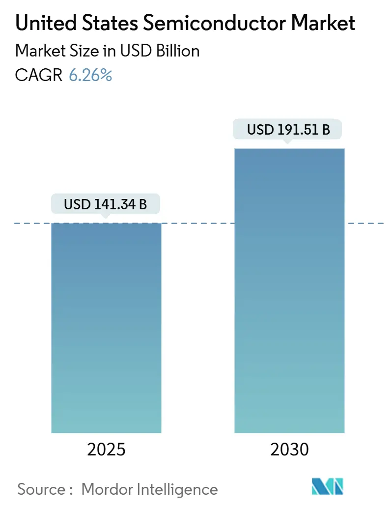
| Market Size (2025) | USD 141.34 Billion |
| Market Size (2030) | USD 191.51 Billion |
| Growth Rate (2025 - 2030) | 6.26% CAGR |
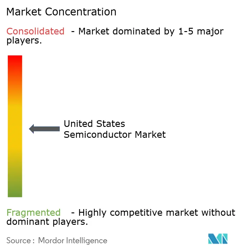
| Market Concentration | Medium |
Major Players *Disclaimer: Major Players sorted in no particular order Image © Mordor Intelligence. Reuse requires attribution under CC BY 4.0. | |
United States Semiconductor Market Analysis by Mordor Intelligence
The United States semiconductor market size is USD 141.34 billion in 2025 and is forecast to expand to USD 191.51 billion by 2030, reflecting a 6.26% CAGR. Robust public-sector incentives under the CHIPS and Science Act, hyperscale spending on AI data centers, and higher semiconductor content in electric vehicles together propel this growth trajectory. Federal grants worth USD 39 billion have already moved 18 new fabs into the construction phase, reversing a long-running decline in domestic wafer output. In parallel, Meta, Amazon, Microsoft, and Alphabet collectively budgeted more than USD 110 billion for AI infrastructure in 2024, creating sustained demand for advanced GPUs, high-bandwidth memory, and optical interconnects. Automotive electrification adds another structural driver as power, sensing, and ADAS processors lift chip value per vehicle toward USD 1 500 by 2030. Against this backdrop, export-control rules and acute engineering-talent shortages remain the main speed bumps for the United States semiconductor market.
Key Report Takeaways
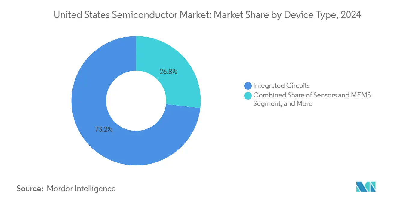
- By device type, integrated circuits led with 73.2% of United States semiconductor market share in 2024. Sensors and MEMS segment is projected to post a 7.89% CAGR through 2030.
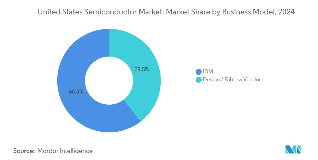
- By business model, IDM companies held 60.5% share of the United States semiconductor market size in 2024. Fabless vendors segment is advancing at a 7.11% CAGR between 2025-2030.
- By end-user industry, data centers controlled 24% share of the United States semiconductor market size in 2024. By end-user industry, AI applications are forecast to record the fastest 8.28% CAGR through 2030.
United States Semiconductor Market Trends and Insights
Drivers Impact Analysis*
| Driver | (~) % Impact on CAGR Forecast | Geographic Relevance | Impact Timeline |
|---|---|---|---|
| Intensifying federal CHIPS Act funding | +1.80% | National, concentrated in Arizona, Texas, New York, Ohio | Medium term (2-4 years) |
| Accelerated AI-centric compute demand from hyperscalers | +2.10% | National, concentrated in data center hubs | Short term (≤ 2 years) |
| Automotive electrification and ADAS semiconductor content surge | +1.20% | National, with automotive manufacturing clusters | Long term (≥ 4 years) |
| Defense-grade rad-hard IC replacement cycle | +0.70% | National, concentrated near defense contractors | Medium term (2-4 years) |
| On-shoring of compound-semiconductor supply chains | +0.90% | National, with SiC/GaN manufacturing centers | Long term (≥ 4 years) |
| Emergence of chiplet/advanced packaging foundry services | +0.80% | National, concentrated in semiconductor hubs | Medium term (2-4 years) |
| Source: Mordor Intelligence | |||
Intensifying Federal CHIPS Act Funding
The CHIPS and Science Act’s USD 39 billion incentive pool has kicked off the largest domestic wafer-capacity buildout on record, with 18 fabs under construction across four states. TSMC alone has committed USD 165 billion to three Arizona plants capable of 2 nm production by 2028, the single biggest foreign direct investment ever made in the country. Intel received USD 8.5 billion to accelerate its Ohio mega-fab that will focus on sub-3 nm nodes vital for AI accelerators and defense-grade microelectronics. Smaller grants to Wolfspeed, ON Semi, and GlobalFoundries extend the footprint to silicon-carbide and specialty RF processes, diversifying the domestic technology base. These projects collectively target more than 60 000 permanent jobs, easing supply-chain exposure to East-Asian foundries and adding a projected 1.8 percentage point lift to the United States semiconductor market CAGR.
Accelerated AI-Centric Compute Demand from Hyperscalers
Meta earmarked USD 65 billion in 2024 for AI data-center buildouts, while Amazon, Microsoft, and Alphabet together budgeted another USD 45 billion the same year. Each GPT-4-class model consumes roughly 25 000 A100 GPUs, driving quarterly HBM volume up 50% and tripling Micron’s data-center revenue in fiscal Q3 2025. Supply now hinges on advanced memory nodes like HBM3E and upcoming HBM4, whose margins outstrip mainstream DRAM by 30-40%. High-speed optical transceivers at 800 G and 1.6 T further swell demand for compound-semiconductor laser drivers. This hyperscaler capex cycle, concentrated in Northern Virginia, Oregon, and Ohio, is expected to add 2.1 percentage points to the United States semiconductor market CAGR during the 2025-2027 window before tapering as AI inference workloads disperse to the edge.
Automotive Electrification and ADAS Semiconductor Content Surge
Semiconductor content per vehicle moved from USD 712 in 2022 to USD 980 in 2024 and is on track for USD 1 500 by 2030. Battery-management ICs, silicon-carbide MOSFETs, and radar processors represent the highest bill-of-materials gains, especially in premium EV models. Tesla’s 4D full self-driving computer delivers 144 TOPS using custom silicon produced on Samsung’s 2 nm node, illustrating how design ownership yields rapid algorithm-hardware co-optimization. Carmakers such as Ford and GM have opened in-house chip-design centers in Austin and Silicon Valley, targeting traction inverters and zonal controllers. These moves broaden the customer base for domestic wafer starts, lifting long-run chip demand by an estimated 1.2 percentage points and strengthening the United States semiconductor market.
Defense-Grade Rad-Hard IC Replacement Cycle
DoD modernization plans covering satellite constellations and hypersonic platforms increased radiation-hardened IC orders by double digits in 2024, with the Defense Logistics Agency awarding USD 126 million for expanding the QML-V supplier roster. Trusted-foundry rules funnel leading-edge defense work to domestic fabs, guaranteeing predictable loadings for niche IDMs that specialize in total-ionizing-dose and single-event-upset immunity. Dual-use spillovers are apparent: radiation-tolerant FPGAs developed for missile defense now ship into commercial space internet constellations. Certification cycles of 18-24 months create medium-term demand visibility, adding 0.7 percentage points to the United States semiconductor market growth outlook.
Restraints Impact Analysis*
| Restraint | (~) % Impact on CAGR Forecast | Geographic Relevance | Impact Timeline |
|---|---|---|---|
| Talent shortage across RF and analog design disciplines | -1.40% | National, concentrated in semiconductor design centers | Long term (≥ 4 years) |
| CAPEX inflation for sub-3nm fabs | -0.90% | National, affecting advanced node manufacturing | Medium term (2-4 years) |
| Export-control restrictions limiting China addressable TAM | -1.10% | National, affecting companies with China exposure | Short term (≤ 2 years) |
| Volatile memory pricing cycles depressing profitability | -0.80% | National, affecting memory manufacturers | Short term (≤ 2 years) |
| Source: Mordor Intelligence | |||
Talent Shortage Across RF and Analog Design Disciplines
McKinsey projects a gap of 67 000-146 000 skilled engineers by 2029, with the steepest deficits in RF front-end and precision-analog layout. U.S. universities graduate fewer than 2 000 RF majors annually while demand already exceeds 8 000 openings, intensifying bidding wars among IDMs, fabless firms, and defense primes. Analog design remains apprenticeship-driven; 35% of senior practitioners will reach retirement age within 10 years, risking institutional memory loss. Visa restrictions further reduce the inflow of foreign graduate talent, tightening the labour market. These variables subtract roughly 1.4 percentage points from United States semiconductor market expansion through higher wage inflation, elongated design cycles, and delayed product ramps.
CAPEX Inflation for Sub-3 nm Fabs
A single extreme-ultraviolet lithography tool now costs USD 200 million, and lead times stretch to 20 months, pushing total sub-3 nm fab outlays into the USD 20-25 billion range. Financing such mega-projects strains corporate balance sheets and forces multi-tranche debt issuance long before revenue commences. The bottleneck is acute: ASML remains the sole EUV supplier, and only three companies TSMC, Samsung, Intel can credibly amortize that scale. Smaller IDMs therefore exit advanced nodes, narrowing domestic competition. This capital overhang trims an estimated 0.9 percentage points from United States semiconductor market CAGR across 2025-2028.
*Our forecasts treat driver/restraint impacts as directional, not additive. The impact forecasts reflect baseline growth, mix effects, and variable interactions.
Segment Analysis
By Device Type: Integrated Circuits Retain Primacy While Sensors Accelerate
Integrated circuits held 73.2% of United States semiconductor market share in 2024, reflecting their central role in compute, memory, and mixed-signal functions. High-bandwidth memory alone delivered nearly 50% sequential revenue growth for Micron in Q3 2025 as hyperscale clusters scaled from 8-GPU to 16-GPU nodes. Logic IC demand jumped as chiplet layouts let designers split compute, I/O, and cache dies, improving yields at advanced nodes. Within power electronics, silicon-carbide MOSFET shipments to EV inverters rose 61% year over year, aided by range gains of 2-3 percentage points. In contrast, discrete semiconductors posted mid-single digit expansion, supported by charger, converter, and relay sockets in residential solar installations.
Sensors and MEMS, the fastest-growing device group, are increasing at a 7.89% CAGR through 2030 on the back of automotive radar and industrial IoT deployments. Premium EVs now ship with 12 camera modules, five radar units, and multiple LiDAR assemblies, each embedding accelerometers and pressure sensors in built-in self-test loops. Industrial clients add vibration and gas-analysis MEMS to predictive-maintenance platforms, lifting unit volumes. Optoelectronics absorb networking capex: 800 G and 1.6 T transceivers rely on high-speed VCSEL driver arrays, while co-packaged optics prototypes pair switch ASICs with silicon-photonics dies. Together, these currents keep integrated circuits dominant in value yet position sensors and MEMS as the momentum play across the United States semiconductor market.


By Business Model: IDM Scale Holds but Fabless Speed Gains Ground
IDM operators controlled 60.5% of United States semiconductor market size in 2024, proving that owning fabs adds strategic leverage during supply-chain shocks. Intel’s Ohio campus targets 5 nm then 2 nm to secure domestic defense and AI workloads, while Texas Instruments expects its USD 60 billion buildout to deliver 90% self-manufactured analog wafers by 2030. In power semiconductors, ON Semi’s vertically integrated SiC line captures inverter sockets in Hyundai and GM vehicles, underscoring the benefit of tool-to-system alignment. Still, fabless firms posted a 7.11% CAGR led by NVIDIA’s rapid iteration on transformer-optimized GPUs and AMD’s chiplet-based EPYC CPUs. These companies extract maximum process-node gains from TSMC’s foundries without carrying multibillion-dollar depreciation charges.
Advanced packaging blurs the historical IDM-fabless divide. NVIDIA’s H200 platform uses TSMC’s CoWoS-R wafer-on-wafer stacking, while Intel’s Foundry Services aims to attract external customers to its EMIB and Foveros flows. Some fabless houses co-invest in OSAT capacity, securing guaranteed lines for 2.5D interposers and HBM stacking. Conversely, IDMs license IP blocks from Arm and Synopsys to reduce internal R&D drag. The coexistence of both models broadens the design-manufacturing talent pool and increases resilience across the United States semiconductor market.
By End-User Industry: Data Centers Dominate as AI Accelerates Edge Adoption
Data-center operators accounted for 24% of United States semiconductor market share in 2024 thanks to AI training rigs that pack as much as 100 kW per rack. Meta’s Grand Teton platform integrates 64 GPUs linked by 800 G optical fabrics, consuming hundreds of HBM stacks per pod. Total server DRAM density per socket exceeded 1 TB in 2025, a 3-fold rise in three years. Custom network processors from Amazon Annapurna and Google Jupiter offload traffic management, widening total addressable silicon. AI applications post the highest 8.28% CAGR through 2030, spanning cloud, automotive, and industrial inference nodes. Tesla’s AI6 chip for on-board autonomy harnesses 8 nmL2 embedded memory to save power while sustaining 600 TOPS performance.
Automotive use cases rank next in momentum as EV sales crest 20% of U.S. light-vehicle volume. Each battery-electric pickup embeds more than 80 power devices plus zonal controllers linked via Gigabit Ethernet, replacing traditional CAN buses. Consumer electronics remain steady, with 5G handsets migrating to 3-nm application processors that incorporate AI co-processors for on-device language translation. Industrial clients increase factory-edge gateways using deterministic Ethernet and real-time AI inferencing for quality inspection. Government and defense orders keep rad-hard and secure-element demand consistent, rounding out a diversified offtake profile for the United States semiconductor market.
Geography Analysis
Arizona hosts the nation’s densest cluster of advanced-logic fabs after TSMC, Intel, and NXP collectively broke ground on more than USD 200 billion of capacity by mid-2025. These investments raise local wafer starts toward 600 000 12-inch equivalents monthly by 2030, anchoring supply for AI accelerators and automotive processors. Texas forms the power-and-analog center: Samsung’s 2 nm line in Taylor, Texas Instruments’ Sherman campus, and ON Semi’s SiC expansion in East Fishkill together serve EV and industrial markets. New York’s USD 100 billion Micron memory campus gives the Northeast a high-density DRAM and NAND hub, pairing with GlobalFoundries’ Malta facility to deliver specialty RF and silicon-photonics output.
California’s Silicon Valley retains design sovereignty, housing more than 45% of U.S. chip-design engineers and 70% of semiconductor venture funding. Seattle and Austin round out the talent triangle, anchored by Amazon’s Annapurna, Microsoft Azure Silicon, and Apple’s custom-silicon teams. Defense-focused IC suppliers cluster near Colorado Springs and Albuquerque, taking advantage of proximity to Air Force and Sandia research centers. North Carolina’s Research Triangle grows into a compound-semiconductor node as Wolfspeed ramps 200 mm SiC wafers, broadening geographic risk distribution across the United States semiconductor market.
The multi-hub model reduces logistic choke points while linking each region to nearby research universities for workforce pipelines. State-level incentive packages often stack onto federal CHIPS grants, lowering effective capital costs by 10-15%. Power-grid capacity, water-recycling mandates, and skilled-labour availability remain the decisive factors shaping where the next wave of fabs lands. Collectively, these regions secure domestic access to logic, memory, analog, and wide-bandgap devices, reinforcing long-term supply resilience for the United States semiconductor market.
Competitive Landscape
Sub-5 nm logic is an oligopoly shared by Intel, TSMC, and Samsung, giving these three outsized influence over design roadmaps and wafer pricing. Intel’s 20% TSMC joint-venture stake discussed in April 2025 exemplifies hybrid strategies that blend internal fabs with external capacity to balance risk. Memory remains consolidated in Micron, Samsung, SK Hynix, and Western Digital-Kioxia; high-bandwidth variants command price premiums and margin stability despite commodity DRAM cycles. Analog and mixed-signal fields look more fragmented: Texas Instruments, Analog Devices, and Infineon together hold under 35% revenue, enabling mid-tier players like Skyworks and MaxLinear to win share through niche performance claims.
Chiplet architectures democratize entry for specialist IP houses. Examples include Marvell’s optical DSPs and SiFive’s RISC-V cores slotting alongside proprietary GPU tiles inside package. OSAT firms Amkor, ASE, and the 3M-backed US-JOINT consortium capture value through 2.5D interposers and wafer-on-wafer assembly. Automotive electrification spurs fresh rivalry as NVIDIA Drive, Mobileye EyeQ6, and Qualcomm Snapdragon Ride vie for centralized ADAS compute sockets. Each platform integrates custom accelerators, secure boot elements, and ISO 26262 safety processing to meet automaker requirements, broadening competition inside the United States semiconductor market.
Strategic moves concentrate on vertical alignment and geographic hedging. Texas Instruments’ USD 60 billion U.S. fab plan ensures over 90% self-manufactured wafers by 2030, insulating it from outsourced supply shocks. Samsung’s USD 16.5 billion Tesla AI6 win showcases capacity reservation as a route to anchor long-term clients. Synopsys’ USD 35 billion acquisition of Ansys builds a full-stack EDA portfolio, ensuring design-for-manufacturing lock-in at emerging process nodes. Taken together, the competitive mosaic rates a “6” on the 1-to-10 concentration scale: the top five vendors command just over 60% combined revenue across key sub-segments yet fragmentation persists in analog, power, and packaging niches.
United States Semiconductor Industry Leaders
Intel Corporation
NVIDIA Corporation
Advanced Micro Devices, Inc.
Qualcomm Incorporated
Texas Instruments Incorporated
- *Disclaimer: Major Players sorted in no particular order

Recent Industry Developments
- July 2025: Samsung Electronics secured a USD 16.5 billion contract to manufacture Tesla’s next-generation AI6 chips through 2033, validating Samsung’s 2 nm automotive roadmap.
- June 2025: Texas Instruments announced a USD 60 billion multilocation analog-fab expansion aimed at 90% internal wafer sourcing by 2030.
- June 2025: Micron Technology posted record USD 9.3 billion Q3 revenue on 50% sequential HBM growth.
- April 2025: Intel and TSMC reached preliminary terms on a 20% TSMC stake in Intel Foundry Services, illustrating the rise of hybrid manufacturing models.


United States Semiconductor Market Report Scope
| Discrete Semiconductors | Diodes | ||
| Transistors | |||
| Power Transistors | |||
| Rectifier and Thyristor | |||
| Other Discrete Devices | |||
| Optoelectronics | Light-Emitting Diodes (LEDs) | ||
| Laser Diodes | |||
| Image Sensors | |||
| Optocouplers | |||
| Other Device Types | |||
| Sensors and MEMS | Pressure | ||
| Magnetic Field | |||
| Actuators | |||
| Acceleration and Yaw Rate | |||
| Temperature and Others | |||
| Integrated Circuits | By Integrated Circuit Type | Analog | |
| Micro | Microprocessors (MPU) | ||
| Microcontrollers (MCU) | |||
| Digital Signal Processors | |||
| Logic | |||
| Memory | |||
| By Technology Node (Shipment Volume Not Applicable) | Less than 3nm | ||
| 3nm | |||
| 5nm | |||
| 7nm | |||
| 16nm | |||
| 28nm | |||
| 28nm | |||
| IDM |
| Design / Fabless Vendor |
| Automotive |
| Communication (Wired and Wireless) |
| Consumer |
| Industrial |
| Computing / Data Storage |
| Data Center |
| AI |
| Government (Aerospace and Defense) |
| By Device Type (Shipment Volume for Device Type is Complementary) | Discrete Semiconductors | Diodes | ||
| Transistors | ||||
| Power Transistors | ||||
| Rectifier and Thyristor | ||||
| Other Discrete Devices | ||||
| Optoelectronics | Light-Emitting Diodes (LEDs) | |||
| Laser Diodes | ||||
| Image Sensors | ||||
| Optocouplers | ||||
| Other Device Types | ||||
| Sensors and MEMS | Pressure | |||
| Magnetic Field | ||||
| Actuators | ||||
| Acceleration and Yaw Rate | ||||
| Temperature and Others | ||||
| Integrated Circuits | By Integrated Circuit Type | Analog | ||
| Micro | Microprocessors (MPU) | |||
| Microcontrollers (MCU) | ||||
| Digital Signal Processors | ||||
| Logic | ||||
| Memory | ||||
| By Technology Node (Shipment Volume Not Applicable) | Less than 3nm | |||
| 3nm | ||||
| 5nm | ||||
| 7nm | ||||
| 16nm | ||||
| 28nm | ||||
| 28nm | ||||
| By Business Model | IDM | |||
| Design / Fabless Vendor | ||||
| By End-user Industry | Automotive | |||
| Communication (Wired and Wireless) | ||||
| Consumer | ||||
| Industrial | ||||
| Computing / Data Storage | ||||
| Data Center | ||||
| AI | ||||
| Government (Aerospace and Defense) | ||||


Key Questions Answered in the Report
What is the revenue projection for the United States semiconductor market by 2030?
The market is projected to reach USD 191.51 billion by 2030, growing at a 6.26% CAGR.
How many new fabrication plants are under construction because of the CHIPS Act?
Eighteen fabs were already under construction nationwide by early 2025.
Which customer segment currently generates the most chip demand in the United States?
Data-center operators lead with 24% of 2024 revenue, driven by AI training clusters.
Why are sensors and MEMS growing faster than other device categories?
Automotive ADAS modules and industrial IoT rollouts are pushing sensor and MEMS volumes at a 7.89% CAGR through 2030.
How does the labor shortage affect U.S. chipmakers?
A projected shortfall of up to 146 000 RF and analog engineers could extend design cycles and increase wage costs, shaving roughly 1.4 percentage points off market growth.
What impact do export-control rules have on U.S. chip revenue?
New restrictions on AI accelerators heading to China could weigh on near-term sales by about USD 11 billion across leading U.S. suppliers.
Page last updated on:


