Semiconductor Equipment Market Size and Share
Market Overview
| Study Period | 2020 - 2031 |
|---|---|
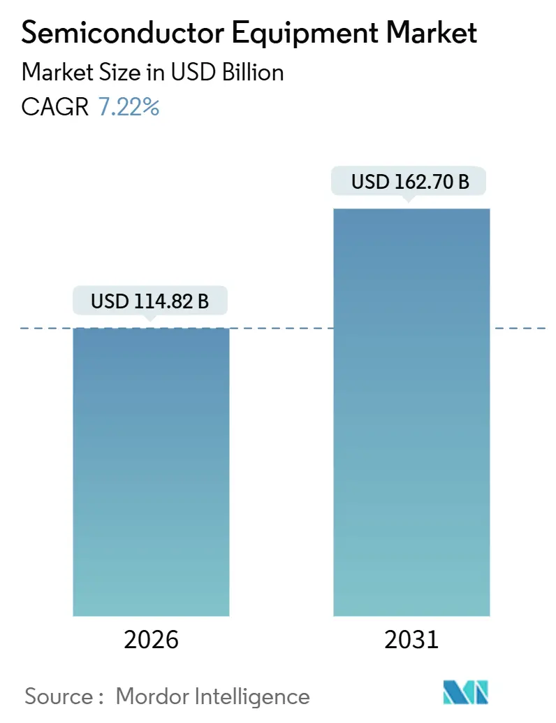
| Market Size (2026) | USD 114.82 Billion |
| Market Size (2031) | USD 162.70 Billion |
| Growth Rate (2026 - 2031) | 7.22% CAGR |
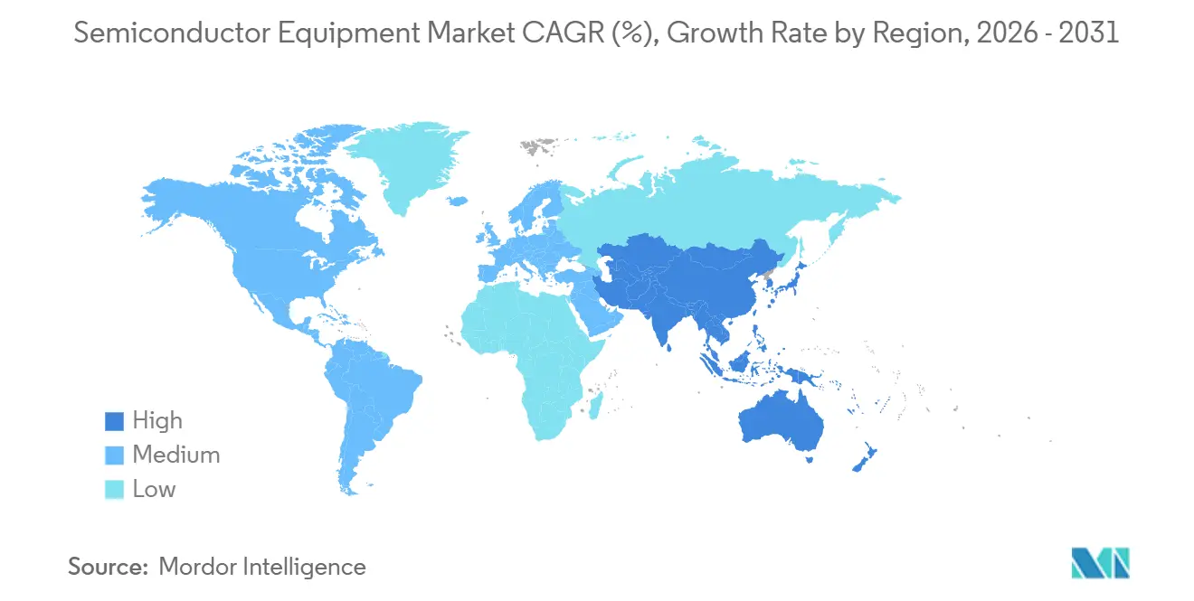
| Fastest Growing Market | Asia Pacific |
| Largest Market | Asia-Pacific |
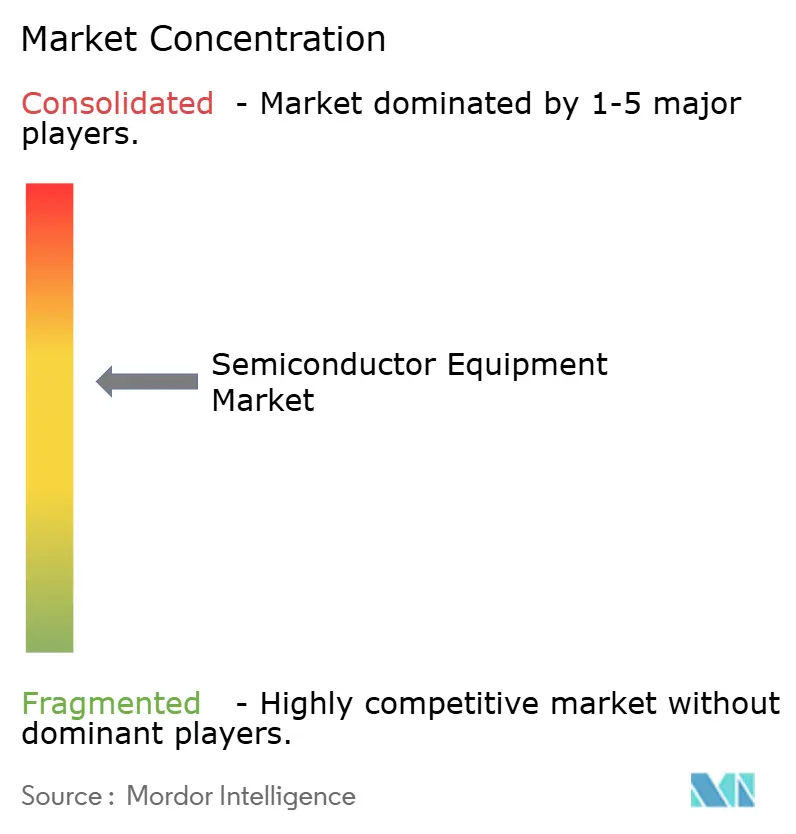
| Market Concentration | Medium |
Major Players *Disclaimer: Major Players sorted in no particular order Image © Mordor Intelligence. Reuse requires attribution under CC BY 4.0. | |
Semiconductor Equipment Market Analysis by Mordor Intelligence
The Semiconductor Equipment Market size is estimated at USD 114.82 billion in 2026, and is expected to reach USD 162.70 billion by 2031, at a CAGR of 7.22% during the forecast period (2026-2031).
This growth reflects the move from consumer-volume manufacturing toward infrastructure-grade precision, where gate-all-around (GAA) transistors and high-numerical-aperture (high-NA) extreme-ultraviolet (EUV) lithography dominate capital plans. Premium pricing for 0.55-NA EUV tools, front-end equipment upgrades that enable 2 nm nodes, and subsidy-backed fab construction together keep the semiconductor equipment market on an expansion path. Meanwhile, specialty 3D heterogeneous-integration lines capture value from chiplet architectures, and sustainability directives spur retrofit demand for energy-efficient chambers. Competitive strategies increasingly hinge on securing supply of scarce photoresists, fluorine gases, and field-service talent, factors that shape both cost structures and shipment timing.
Key Report Takeaways
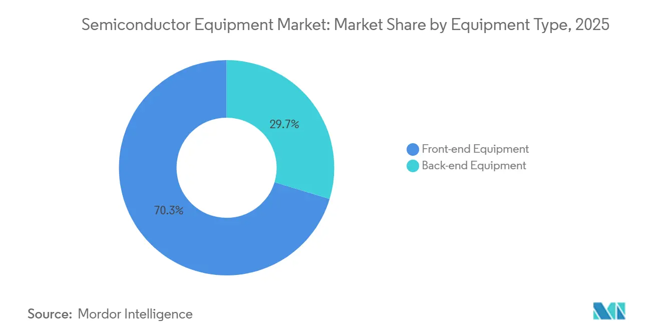
- By equipment type, front-end tools led with 70.33% of semiconductor equipment market share in 2025; the same category is forecast to grow at an 8.16% CAGR through 2031.
- By supply-chain participant, foundries held 52.92% revenue share in 2025, while outsourced semiconductor assembly and test (OSAT) providers record the highest projected 7.84% CAGR to 2031.
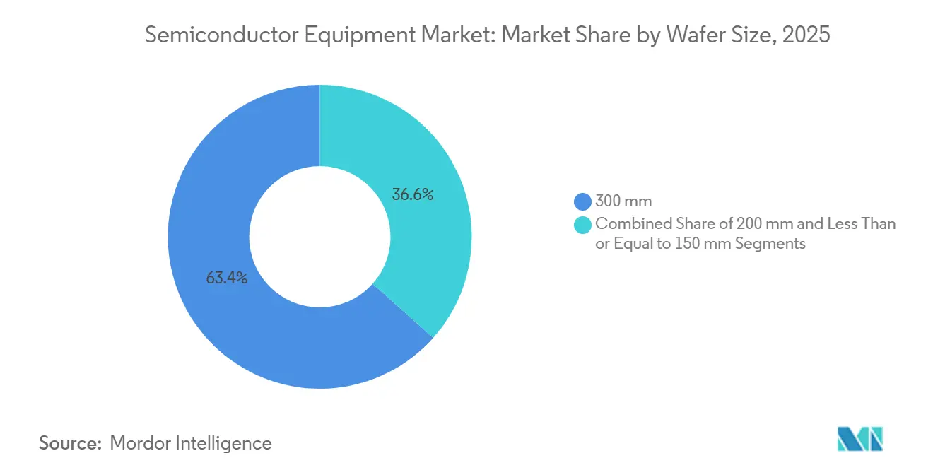
- By wafer size, 300 mm substrates commanded 63.42% of the semiconductor equipment market size in 2025 and are set to expand at an 8.02% CAGR between 2026 and 2031.
- By end-use industry, computing applications captured 32.12% share of the semiconductor equipment market size in 2025; automotive and mobility equipment demand is growing at an 8.44% CAGR through 2031.
- By geography, Asia-Pacific accounted for 52.97% revenue share in 2025 and is advancing at a 9.07% CAGR, the fastest across all regions.
Note: Market size and forecast figures in this report are generated using Mordor Intelligence’s proprietary estimation framework, updated with the latest available data and insights as of January 2026.
Global Semiconductor Equipment Market Trends and Insights
Drivers Impact Analysis*
| Driver | (~) % Impact on CAGR Forecast | Geographic Relevance | Impact Timeline |
|---|---|---|---|
| Surging demand for advanced consumer electronics and smartphones | +0.9% | Global, with concentration in Asia-Pacific (China, India, Southeast Asia) | Short term (≤ 2 years) |
| Rapid AI-, IoT- and edge-device node investments | +1.8% | Global, led by North America and Asia-Pacific (Taiwan, South Korea, Japan) | Medium term (2-4 years) |
| Government subsidy waves (CHIPS Act, EU Chips Act, etc.) boosting tool CAPEX | +1.5% | North America and Europe, with spillover to allied Asia-Pacific partners | Medium term (2-4 years) |
| Transition to GAA and High-NA EUV necessitating new toolsets | +1.3% | Global, concentrated in leading-edge fabs (Taiwan, South Korea, United States) | Long term (≥ 4 years) |
| Sustainability mandates driving green-fab retrofit tools | +0.6% | Europe and North America, expanding to Asia-Pacific | Long term (≥ 4 years) |
| 3D heterogeneous-integration packaging demand spike | +1.1% | Global, with early adoption in Taiwan, South Korea, and United States | Medium term (2-4 years) |
| Source: Mordor Intelligence | |||


Rapid AI, IoT and Edge-Device Node Investments
Artificial-intelligence inference workloads and distributed edge computing are pushing process nodes below 5 nm, where equipment intensity per wafer rises sharply. OpenAI committed USD 500 million in 2025 to secure advanced-node capacity at Taiwan Semiconductor Manufacturing Company (TSMC), while Microsoft and Amazon Web Services each placed multi-billion-dollar reservations for 3 nm custom silicon. ASML reported a 40% year-on-year increase in EUV tool shipments during the first three quarters of 2025. In contrast, IoT devices stay on mature 28 nm and 40 nm lines, yet emerging edge-AI accelerators combine radio-frequency layers at 22 nm with digital logic at 7 nm, forcing fabs to install heterogeneous packaging lines that merge dissimilar dies. The International Technology Roadmap for Semiconductors projects that by 2028, more than half of high-performance chips will adopt chiplet architectures, each requiring novel assembly, test, and advanced packaging equipment.[1]IEEE, “International Technology Roadmap for Semiconductors,” Ieee.org
Government Subsidy Waves Boosting Tool CAPEX
Legislation such as the United States CHIPS and Science Act and the EU Chips Act compresses procurement cycles that formerly spanned two years. Intel secured USD 8.5 billion in grants plus USD 11 billion in loan guarantees for new fabs in Ohio and Arizona, committing to purchase over 200 leading-edge tools by 2028. Micron, Samsung and Rapidus received similar state support in New York, South Korea and Japan, respectively. India’s Ministry of Electronics and Information Technology approved USD 2.75 billion for Micron’s Gujarat assembly facility, spurring orders for back-end platforms. These incentives front-load demand into the 2026-2028 window, lifting the semiconductor equipment market yet raising utilization-rate questions once subsidies taper.
Transition to GAA and High-NA EUV Toolsets
Gate-all-around devices replace finFETs at the 2 nm node and below, demanding atomic-layer deposition (ALD) tools with sub-angstrom control and selective-etch chemistries that spare adjacent nanosheets. TSMC’s first 2 nm production line deployed more than 50 new ALD chambers in late 2025. Samsung reported 95% yield on its 2 nm pilot wafers and ordered 30 additional deposition and etch tools to sustain a 2026 ramp. High-NA EUV, operating at 0.55 numerical aperture, shipped its inaugural system to Intel in December 2025 with a USD 400 million price tag and facility modifications for vibration and thermal stability. GAA adds roughly 30% more deposition and etch steps than finFET, creating a durable replacement cycle that supports the semiconductor equipment market through 2031.
3D Heterogeneous-Integration Packaging Demand Spike
Chiplet architectures are transferring performance scaling from monolithic die shrinks to back-end packaging. TSMC doubled its chip-on-wafer-on-substrate capacity in 2025, installing over 40 hybrid-bonding tools from Besi and EVG. Intel’s Foveros Direct technology stacks compute tiles on input-output dies at 25 µm bump pitch, requiring precision aligners and thermal compression bonders from Kulicke and Soffa and ASM Pacific Technology. The Universal Chiplet Interconnect Express standard, ratified in August 2025, is accelerating multi-vendor ecosystems and expanding OSAT capital intensity.
Restraints Impact Analysis*
| Restraint | (~) % Impact on CAGR Forecast | Geographic Relevance | Impact Timeline |
|---|---|---|---|
| Extremely high CAPEX and long pay-back cycles | -0.8% | Global, particularly acute in emerging fab regions (India, Middle East, Southeast Asia) | Long term (≥ 4 years) |
| Specialty-material supply bottlenecks delaying tool shipments | -1.2% | Global, with concentration in Asia-Pacific and Europe | Short term (≤ 2 years) |
| Export-control restrictions on China-bound tools | -1.4% | China, with spillover effects on global equipment suppliers (Netherlands, Japan, United States) | Medium term (2-4 years) |
| Acute shortage of skilled field-service engineers | -0.9% | North America and Europe, expanding to Asia-Pacific | Medium term (2-4 years) |
| Source: Mordor Intelligence | |||
Export-Control Restrictions on China-Bound Tools
From September 2025, the Netherlands, the United States, and Japan tightened licensing for lithography, deposition, and etch platforms capable of sub-14 nm patterning, blocking shipments to Chinese fabs.[2]Government of the Netherlands, “Export-Control Regulations,” Government.nl China’s equipment imports fell 28% year-on-year in 1H 2025, while local suppliers Advanced Micro-Fabrication Equipment and Naura Technology Group grew 42% as fabs accepted older-generation domestic tools. The split forces Western vendors to concentrate high-end sales in Taiwan, South Korea, and North America, while risking long-term share erosion once Chinese producers close the technology gap.
Specialty-Material Supply Bottlenecks Delaying Tool Shipments
Capacity shortfalls in high-NA EUV photoresists, nitrogen-trifluoride etch gases and rare-earth polishing slurries extend commissioning timelines even when hardware arrives on schedule. JSR warned in June 2025 that high-NA resist output would stay tight into mid-2026. A fire at a Taiwanese NF₃ plant lifted gas prices by 22% in 2025, prompting delayed acceptances for deposition chambers. Cerium-oxide export quotas raised slurry costs by 18%, forcing fabs to run pads longer at the expense of higher defect densities.[3]Financial Times, “Rare-Earth Export Quotas,” Ft.com
*Our forecasts treat driver/restraint impacts as directional, not additive. The impact forecasts reflect baseline growth, mix effects, and variable interactions.
Segment Analysis
By Equipment Type: Front-End Dominance Anchored by Lithography Intensity
Front-end platforms captured 70.33% semiconductor equipment market share in 2025 and are tracking an 8.16% CAGR through 2031. Lithography alone accounted for 35% of total outlays in 2025, as fabs migrated from 0.33-NA to 0.55-NA EUV systems priced at over USD 400 million each. Etch revenues climbed 9.2% in the same year because GAA structures require selective removal of sacrificial silicon-germanium. Deposition tools, particularly ALD and CVD, grew 8.7% on 2 nm uptake. Metrology and inspection expanded 10.1% as inline defect detection becomes mandatory below 10 nm.
Back-end tools accounted for 29.67% of the semiconductor equipment market in 2025 and will grow at a 6.8% CAGR. Hybrid-bonding equipment for chiplet assembly rose 11% in 2025, while high-bandwidth-memory testers advanced 14% amid 12-die stack adoption. Cleaning and photoresist processing units each improved 7.4%. Although packaging gains relevance, the capital intensity of leading-edge lithography ensures front-end platforms preserve revenue leadership through 2031.


By Supply-Chain Participant: Foundries Lead, OSATs Accelerate
Foundries absorbed 52.92% of 2025 equipment purchases, underpinned by TSMC’s USD 32 billion and Samsung’s USD 22 billion capex programs. Integrated device manufacturers (IDMs) followed with 28.24%, dominated by Intel’s 18-angstrom and 20-angstrom projects. OSATs held 18.84% but are poised for a 7.84% CAGR as chiplet designs shift complexity toward packaging.
This structure is reshaping supply priorities. Foundries focus on EUV, ALD, and selective-etch, whereas OSATs deploy hybrid-bonding, through-silicon-via, and wafer-level fan-out lines. Rising OSAT capital intensity, from 12% of revenue in 2020 to 16% in 2025, signals a gradual rebalancing of value capture across the semiconductor equipment market.
By Wafer Size: 300 mm Primacy Reinforced by Leading-Edge Economics
The 300 mm segment accounted for 63.42% of 2025 revenue, expanding at an 8.02% CAGR, as 2 nm logic and high-bandwidth memory rely exclusively on this diameter. Intel’s Ohio fab, due in 2027, installs 200 tools optimized for 300 mm wafers, highlighting format lock-in. Conversely, 200 mm lines carry 24.16% share, growing 5.9% on continued analog and power demand that favors silicon-carbide epitaxy. Sub-150-mm wafers serve niche MEMS and compound devices, with a 12.42% share.
Economics drive the split, 300 mm substrates cut die cost by 35% versus 200 mm at 2 nm despite rising defect density, while power modules remain on 200 mm owing to material-quality limits. Suppliers, therefore, maintain parallel 300 mm and 200 mm portfolios, fragmenting scale economies.
By End-Use Industry: Computing Leads, Automotive Surges
Computing captured 32.12% of equipment demand in 2025 as Nvidia’s 208-billion-transistor Blackwell GPUs consumed over 500 wafer starts weekly. Automotive and mobility, holding 19.8%, are the fastest-growing at 8.44% CAGR, propelled by silicon-carbide inverters and advanced driver-assistance sensors. Communications stood at 22.4% with 5G base station rollouts, while consumer electronics slipped to 15.6% amid lengthening smartphone cycles. Industrial and IoT rounded out demand at 10.08%, driven by factory automation in Germany and Japan.
The result is a pivot from consumer to infrastructure use cases. Automotive customers demand longer tool lifecycles, and hyperscalers require aggressive throughput guarantees, compelling suppliers to bundle predictive-maintenance software with capital sales.
Geography Analysis
Asia-Pacific led the semiconductor equipment market with a 52.97% share in 2025 and is set to post a 9.07% CAGR through 2031. Taiwan alone imported USD 28 billion of tools in 2025 as TSMC installed more than 100 EUV systems across three fabs. South Korea followed with USD 19 billion in spend, split between foundry and memory. Although China’s imports dropped from USD 33 billion in 2024 to USD 24 billion in 2025, domestic vendors shipped over 600 units to local fabs, partially offsetting the impact of export controls.
North America accounted for 24.8% of 2025 revenue and will grow at an 8.3% CAGR, accelerated by the CHIPS Act funding that de-risks Intel, Micron, and Texas Instruments expansions. Europe held 18.6% and is advancing at 7.1% as the European Semiconductor Manufacturing Company builds a EUR 10 billion Dresden fab focused on automotive nodes. The Middle East and Africa together captured 2.1%, driven by sovereign diversification programs, while South America’s 1.53% share stems mainly from Brazilian assembly lines.
Differences in subsidy structures and geopolitical risk are shaping regional allocations of tools. Allied regions move ahead with high-NA EUV, whereas China prioritizes indigenous 28 nm and 14 nm capacity, reinforcing a bifurcated global landscape within the broader semiconductor equipment market.

Competitive Landscape
Five companies - ASML, Applied Materials, Tokyo Electron, Lam Research, and KLA Corporation - hold a significant share of front-end revenue, reflecting a moderate concentration structure typical of the semiconductor equipment industry. ASML maintains a high share in EUV lithography, delivering 90 systems in 2025 and defending its position with over 6,000 patents. Applied Materials and Tokyo Electron together control more than half of the deposition segment, while Lam Research holds a considerable share of the etch segment.
Yet white-space opportunities persist. Besi and EVG command early leadership in hybrid bonding for chiplets, and green-fab retrofit tools gain attention as sustainability metrics tighten. Chinese vendors AMEC and Naura expanded 42% in 2025 by supplying 28 nm-capable etchers at 30% discounts, eroding multinational share in mature-node fabs. Export-control regimes accelerate this divergence. Western suppliers focus on allied geographies for high-NA adoption, while Chinese firms fortify domestic ecosystems, fragmenting the semiconductor equipment market into parallel technology tiers.
Supplier strategies emphasize capacity expansion and service-lifecycle differentiation. Applied Materials added 120 ALD chamber lines in Singapore, while Lam Research introduced a GAA-optimized dielectric-etch system that removes silicon-germanium with sub-angstrom selectivity. KLA launched an e-beam inspection platform capable of sub-10 nm defect capture, aligning metrology offerings with high-NA process windows.
Semiconductor Equipment Industry Leaders
ASML Holding NV
Applied Materials Inc.
Lam Research Corp.
Tokyo Electron Ltd.
KLA Corp.
- *Disclaimer: Major Players sorted in no particular order

Recent Industry Developments
- December 2025: ASML shipped its first high-NA EUV system to Intel’s Oregon development fab, marking the commercial debut of 0.55-NA tools priced above USD 400 million.
- November 2025: Samsung Foundry verified 95% yield on 2 nm GAA wafers and ordered 30 additional ALD and selective-etch tools to support a 2H 2026 volume ramp.
- October 2025: Applied Materials completed a USD 450 million deposition-tool factory expansion in Singapore, lifting annual ALD chamber capacity to 120 units.
- September 2025: The Netherlands broadened export controls to cover deep-ultraviolet immersion lithography systems capable of sub-14 nm patterning, cutting ASML’s 2026 China revenue outlook by 25%.
- August 2025: TSMC commenced 2 nm volume production in Hsinchu, installing more than 50 ALD chambers and selective-etch tools for GAA transistors.


Research Methodology Framework and Report Scope
Market Definitions and Key Coverage
Our study treats the semiconductor equipment market as all new, factory-built front-end tools (lithography, etch, deposition, clean, metrology/inspection) and back-end systems (assembly, packaging, electrical test) that are sold to integrated device makers, foundries, or outsourced assembly and test firms. Values are expressed in USD billions at the point of sale.
Scope exclusion: refurbished tools, spare parts, and consumables are outside the frame.
Segmentation Overview
- By Equipment Type
- Front-end Equipment
- Lithography Equipment
- Etch Equipment
- Deposition Equipment
- Metrology/Inspection Equipment
- Cleaning Equipment
- Photoresist Processing Equipment
- Other Equipment Types
- Back-end Equipment
- Test Equipment
- Assembly and Packaging Equipment
- Front-end Equipment
- By Supply-Chain Participant
- Integrated Device Manufacturer (IDM)
- Foundry
- Outsourced Semiconductor Assembly and Test (OSAT)
- By Wafer Size
- 300 mm
- 200 mm
- Less than or Equal to 150 mm
- By End-Use Industry
- Computing and Data- Center
- Communications (5G,RF)
- Automotive and Mobility
- Cosumer Electronics
- Industrial and Others
- By Geography
- North America
- United States
- Canada
- Mexico
- South America
- Brazil
- Argentina
- Rest of South America
- Europe
- Germany
- United Kingdom
- France
- Italy
- Spain
- Rest of Europe
- Asia-Pacific
- China
- Japan
- India
- South Korea
- ASEAN
- Rest of Asia-Pacific
- Middle East
- Saudi Arabia
- United Arab Emirates
- Rest of Middle East
- Africa
- South Africa
- Nigeria
- Rest of Africa
- North America
Detailed Research Methodology and Data Validation
Primary Research
We interviewed process engineers in Asia-Pacific fabs, capital-equipment procurement heads in North America, and packaging-line managers in Europe. Conversations clarified live wafer-start plans, tool lead times, and expected photoresist moves, allowing our team to challenge secondary data and stress test node-mix assumptions.
Desk Research
Analysts first assembled macro and sector data from tier-1 public sources such as SEMI WWSEMS statistics, SIA trade releases, WSTS semiconductor billings, national customs shipment records, and central bank capex series. Corporate 10-K filings, investor decks, and patent analytics drawn from Questel complemented the public set, while news archives on Dow Jones Factiva supplied deal flow and fab announcements. These threads established baseline volumes, average selling prices, and technology-node timing. Numerous other outlets were reviewed; the list above is illustrative, not exhaustive.
Market-Sizing & Forecasting
A top-down reconstruction linking global wafer-start capacity, average tool count per 1,000 wph line, and blended ASP benchmarks generated the initial size. Select bottom-up checks, supplier roll-ups and sample channel ASP × unit flows, fine-tuned totals. Key variables include quarterly fab capex, 300 mm build-out pace, EUV scanner penetration, test intensity ratios, and regional incentive disbursements. A multivariate regression weighing capex, smartphone units, EV silicon content, and memory price cycles projects demand to 2030; scenario analysis flags upside from high-NA EUV adoption. Gaps in sub-segment data are bridged with normalized tool-to-wafer multipliers vetted through expert calls.
Data Validation & Update Cycle
Outputs pass anomaly screens against SEMI billings and customs tallies, then flow through a two-step analyst review. Models refresh each year, with interim updates triggered by material fab announcements; a last-mile check ensures clients receive the latest view.
Why Mordor's Semiconductor Equipment Baseline Inspires Confidence
Published numbers often diverge because firms choose dissimilar tool scopes, currency bases, or forecast cadences.
Key gap drivers here include whether back-end testers are counted, how aggressively year-one ASP inflation is applied, and if fab-facility equipment is bundled. Mordor Intelligence anchors scope on production-critical front and back-end tools only, applies audited currency rates, and refreshes models annually, yielding a steadier baseline.
Benchmark comparison
| Market Size | Anonymized source | Primary gap driver |
|---|---|---|
| USD 124.0 B | Mordor Intelligence | - |
| USD 118.8 B | Regional Consultancy A | Excludes electrical test gear and applies 2024 node mix without update |
| USD 127.8 B | Global Consultancy A | Bundles fab-facility systems and uses aggressive 8% ASP uplift |
These comparisons show that while other publishers tilt conservative or optimistic depending on inclusion choices, Mordor's disciplined variable set and annual refresh deliver a balanced, transparent starting point for strategic decisions.


Key Questions Answered in the Report
What is the projected value of the semiconductor equipment market in 2031?
The market is forecast to reach USD 162.70 billion by 2031, supported by a 7.22% CAGR.
Which segment captures the largest semiconductor equipment market share today?
Front-end equipment commands 70.33% of 2025 revenue, driven by lithography, deposition and etch demand.
Why are 300 mm wafers critical for leading-edge production?
They lower die cost by 35% at the 2 nm node and concentrate all EUV and GAA investments, pushing the 300 mm share to 63.42% in 2025.
How do export controls impact semiconductor equipment suppliers?
Controls restrict advanced tool shipments to China, shifting high-end demand to allied regions and encouraging Chinese fabs to adopt domestic alternatives that trail by 2–3 generations.
What opportunities arise from heterogeneous-integration packaging?
Chiplet architectures spur investment in hybrid-bonding, through-silicon-via and wafer-level fan-out equipment, generating double-digit growth for back-end tool suppliers.
Page last updated on:


