Taiwan LED Epitaxial Wafer Market Size and Share
Market Overview
| Study Period | 2020 - 2031 |
|---|---|
| Forecast Data Period | 2026 - 2031 |
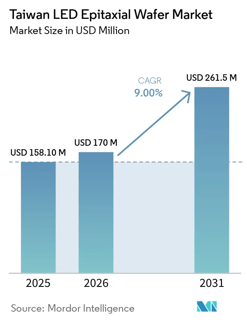
| Base Year Market Size (2025) | USD 158.10 Million |
| Market Size (2026) | USD 170 Million |
| Market Size (2031) | USD 261.5 Million |
| Growth Rate (2026 - 2031) | 9.00% CAGR |
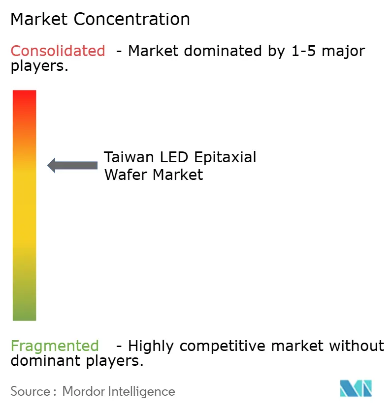
| Market Concentration | Medium |
Major Players *Disclaimer: Major Players sorted in no particular order Image © Mordor Intelligence. Reuse requires attribution under CC BY 4.0. | |
Taiwan LED Epitaxial Wafer Market Analysis by Mordor Intelligence
The Taiwan LED epitaxial wafer market size was valued at USD 158.1 million in 2025 and estimated to grow from USD 170.0 million in 2026 to reach USD 261.5 million by 2031, at a CAGR of 9% during the forecast period (2026-2031). Growth is anchored in the island’s transition away from commodity general-lighting toward higher-margin fields such as mini-LED and micro-LED backlighting, automotive adaptive headlamps, and deep-ultraviolet sterilization. Clustered know-how in Hsinchu Science Park and the Southern Taiwan Science Park accelerates process transfers from four-inch to 200 mm GaN-on-Si, allowing fabs to meet global display makers’ multisourcing mandates. GaN epitaxy remains the revenue cornerstone, yet AlGaN for UV-C LEDs is scaling quickly as healthcare and water-treatment policies phase out mercury lamps. Competitive pressure from subsidized mainland Chinese capacity intensifies pricing in low-spec grades, pushing Taiwanese firms to protect margin through automotive qualifications and 200 mm conversions.
Key Report Takeaways
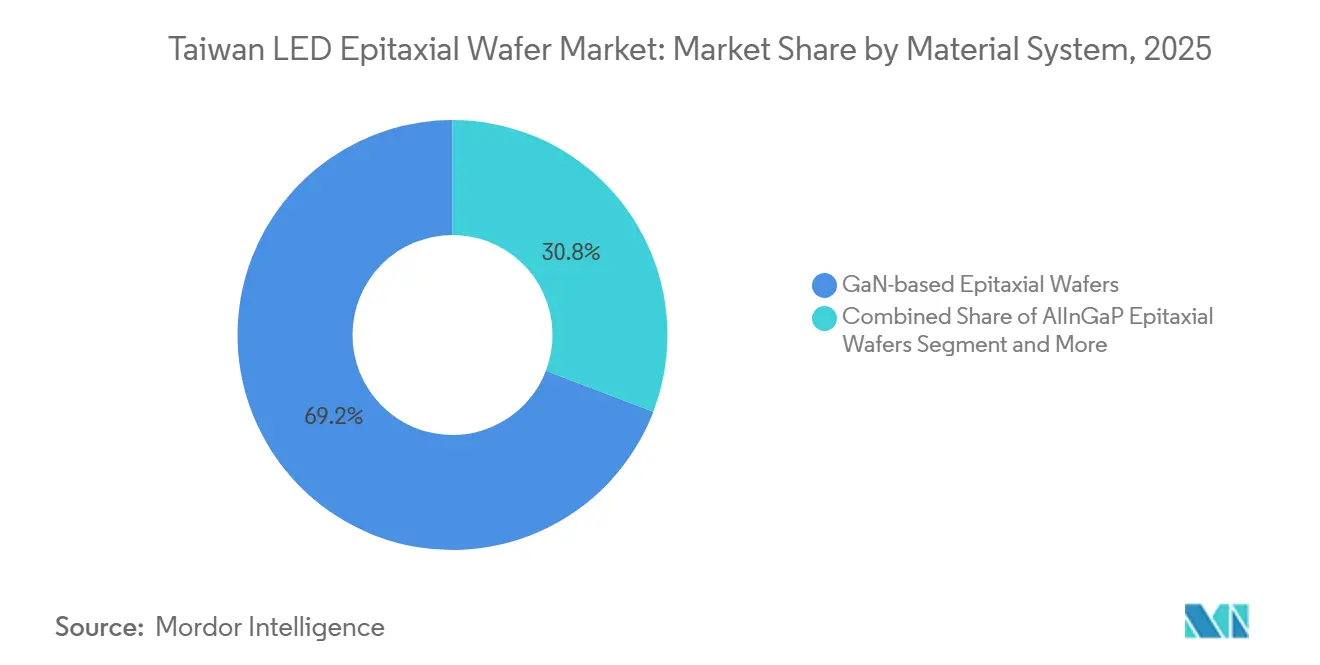
- By material system, GaN maintained 69.20% of the Taiwan LED epitaxial wafer market share in 2025, while AlGaN is forecast to post the fastest 12.40% CAGR through 2031.
- By substrate, sapphire captured 57.20% revenue in 2025; silicon substrates are advancing at a 12.60% rate through 2031.
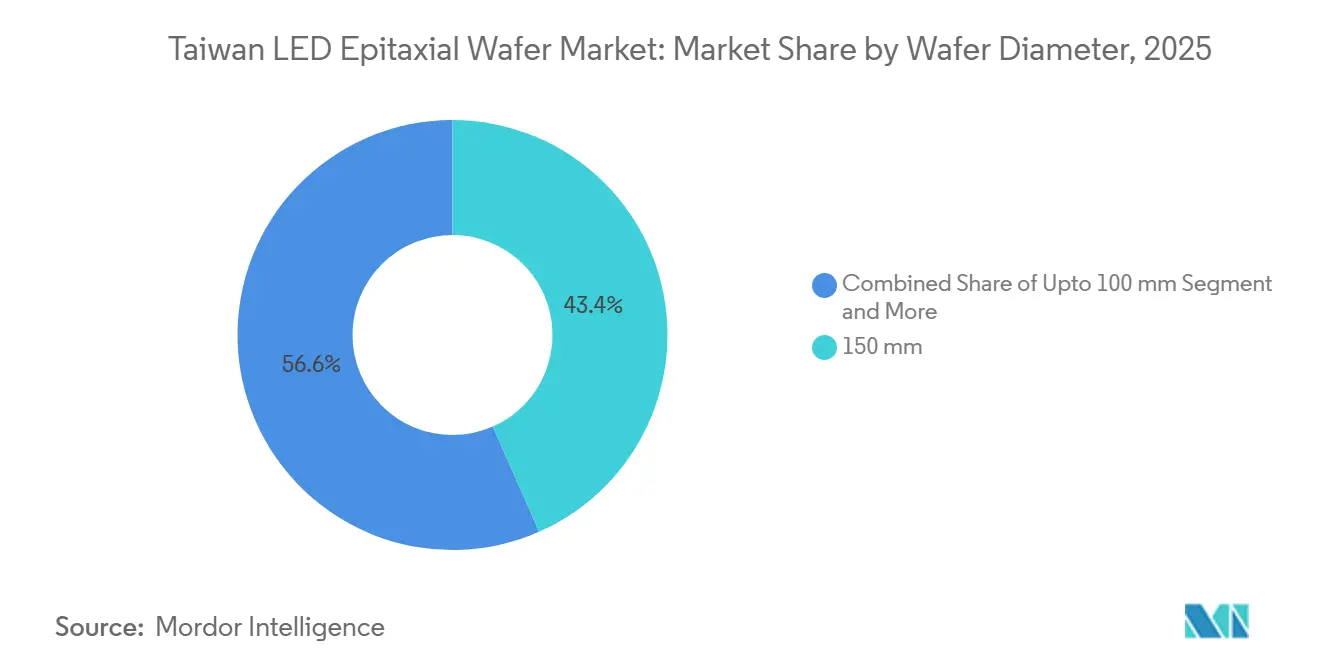
- By wafer diameter, the 150 mm format represented 43.40% of 2025 shipments, and the 200 mm and Above category is projected to expand at a 13.80% CAGR to 2031.
- By application, general lighting led with 42.90% revenue in 2025, whereas displays and backlighting are set to rise at a 13.50% CAGR through 2031.
Note: Market size and forecast figures in this report are generated using Mordor Intelligence’s proprietary estimation framework, updated with the latest available data and insights as of January 2026.
Taiwan LED Epitaxial Wafer Market Trends and Insights
Drivers Impact Analysis*
| DRIVER | (~) % IMPACT ON CAGR FORECAST | GEOGRAPHIC RELEVANCE | IMPACT TIMELINE |
|---|---|---|---|
| Growing Demand for Mini and Micro-LED Displays | +2.8% | Taiwan, South Korea, Japan; spill-over to Vietnam and Thailand | Medium term (2–4 years) |
| Government Incentives for Domestic Semiconductor Manufacturing | +1.9% | National; focused on Hsinchu, Southern Taiwan, and Kaohsiung clusters | Long term (≥4 years) |
| Rapid Penetration of UV-C LED Sterilization Systems | +1.5% | Global healthcare and municipal water sectors | Short term (≤2 years) |
| Expansion of Automotive LED Headlamp Production | +1.3% | Export-oriented output for Europe and North American OEMs | Medium term (2–4 years) |
| Emergence of Smart Lighting in Industrial IoT Environments | +0.8% | Asia Pacific factories, selective Europe uptake | Long term (≥4 years) |
| Localization of GaN-on-Si Processes to Reduce Costs | +0.7% | Taiwan and mainland China | Medium term (2–4 years) |
| Source: Mordor Intelligence | |||
Growing Demand for Mini and Micro-LED Displays
Apple’s migration to mini-LED backlighting in premium tablets and notebooks spurred large-volume orders for Taiwanese epiwafers in 2024-2025, forcing fabs to tighten wavelength-uniformity bins and adopt advanced optical inspection. Samsung Display’s validation of mainland Chinese wafers added pricing tension, so Taiwanese suppliers accelerated 200 mm transitions to sustain their quality premium. Micro-LED remains in pilot scale, yet ALLOS Semiconductors’ 200 mm GaN-on-Si platform, deployed with Ennostar in 2026, signals workable yield for smart-watch and AR microdisplays.[1]ALLOS Semiconductors, “ALLOS and Ennostar Partner on 200 mm GaN-on-Si for MicroLED,” allos-semi.com Mini-LEDs are fueling growth, while micro-LEDs are paving the way for future design victories. Brands, in their quest for heightened peak brightness and wary of OLED burn-in, are turning their gaze to Taiwan's LED epitaxial wafer scene, underscoring its pivotal role in securing a reliable second-source supply.
Government Incentives for Domestic Semiconductor Manufacturing
The National Development Council’s Ten Major AI Infrastructure Projects earmark NTD 15 trillion (USD 480 billion) through 2040, with compound-semiconductor carve-outs that lower borrowing costs for new 200 mm cleanrooms and MOCVD tools. Accelerated depreciation on GaN-on-Si equipment purchased between 2024-2026 further compresses payback periods. Kaohsiung’s silicon-photonics cluster, targeting NTD 7 trillion (USD 224 billion) output by 2028, extends incentives to LED epiwafers for co-packaged optics and automotive LiDAR. While Taiwan imposes no local-content mandates, streamlined environmental permits and concessional loans tilt capital formation toward domestic fabs. These policy tailwinds lift utilization, sustain R&D budgets, and reinforce the island’s centrality to global optoelectronics.
Rapid Penetration of UV-C LED Sterilization Systems
Healthcare disinfection protocols and municipal water standards are pivoting away from mercury lamps ahead of the Minamata Convention’s 2027 deadline, catalyzing demand for AlGaN epiwafers emitting at 260-280 nm. External-quantum-efficiency gains after contact-layer refinements have crossed key procurement thresholds for point-of-use treatment and HVAC retrofits. Tier-one chipmakers such as Seoul Viosys and Nichia outsource overflow epitaxy to Taiwanese foundries to diversify supply risks and deepen local order books.[2]Seoul Viosys Co., “UV-C LED Technology,” seoulviosys.com Although absolute volumes remain modest versus lighting or displays, gross margins are superior because aluminum-rich recipes require low-defect AlN templates and extended MOCVD cycle times. The Taiwan LED epitaxial wafer market is therefore positioned to monetize environmental regulation as a premium niche.
Expansion of Automotive LED Headlamp Production
Adaptive driving beam headlamps require tight wavelength control and defect-free epitaxial layers, areas where Taiwan’s process discipline stands out. Edison Opto and Everlight Electronics validated their automotive-grade chips with Continental AG and Valeo in 2025, driving a notable increase in export momentum. Automotive-grade GaN wafers command a price premium over general lighting grades, helping offset relatively modest volume expansion. As UNECE Regulation 123 expands across more vehicle categories, demand for high-uniformity epitaxial wafers is set to rise, reinforcing a stable revenue base for fabs already compliant with IATF 16949.[3]UNECE, “Regulation 123 on Adaptive Driving Beam Systems,” unece.org Ongoing investment in reliability testing and full traceability will remain a key differentiator, particularly as manufacturers compete against cost-focused entrants from mainland China.
Restraints Impact Analysis*
| RESTRAINT | (~) % IMPACT ON CAGR FORECAST | GEOGRAPHIC RELEVANCE | IMPACT TIMELINE |
|---|---|---|---|
| Rising Competition from Mainland China’s Epitaxy Capacity | -1.8% | Taiwan and South Korea, cascading to Southeast Asia | Short term (≤2 years) |
| Technical Barriers in Mass Transfer for Micro-LED | -1.2% | Global, acute in Taiwan and South Korea pilot lines | Medium term (2–4 years) |
| Volatility in Sapphire Substrate Prices | -0.6% | Taiwan, Mainland China, Japan | Short term (≤2 years) |
| Environmental Concerns Around HF and NH₃ Waste Streams | -0.4% | National, stricter enforcement in science parks | Long term (≥4 years) |
| Source: Mordor Intelligence | |||
Rising Competition from Mainland China’s Epitaxy Capacity
San’an Optoelectronics and HC SemiTek added more than 100 new MOCVD reactors during 2024-2025, enabling price cuts of 15-20% in commodity grades that compress Taiwanese margins. [4]San’an Optoelectronics Co., “Corporate Information,” sanan-e.comSubsidized credit, land grants, and tax holidays under Beijing’s manufacturing agenda allow Chinese fabs to sustain aggressive pricing while still covering depreciation. Taiwanese suppliers counter by pursuing automotive and micro-LED qualifications that set higher performance hurdles that Chinese peers have yet to meet. However, the pricing overhang ripples through every downstream assembler, limiting their ability to pass cost increases up the chain. Unless Taiwan maintains process differentiation, share erosion could accelerate.
Technical Barriers in Mass Transfer for Micro-LED
Large-area micro-LED displays demand transfer of millions of 5-50 µm dies at yields exceeding 99.995%, a threshold current stamp, laser lift-off, and fluidic methods struggle to meet. [5]IEEE Transactions on Electron Devices, “Mass Transfer Technologies for Micro-LED Displays,” ieeexplore.ieee.org Equipment vendors have yet to prove throughput above 10 million placements per hour at an acceptable cost, delaying smartphone and television adoption. Even with 200 mm GaN-on-Si wafers lowering die cost, transfer inefficiency keeps total module economics uncompetitive versus OLED. Taiwanese fabs, therefore, face uncertainty on capital-spending timing, as premature capacity build-outs risk underutilization. The technological bottleneck caps near-term upside for micro-LED and tempers the growth trajectory of the Taiwan LED epitaxial wafer market.
*Our forecasts treat driver/restraint impacts as directional, not additive. The impact forecasts reflect baseline growth, mix effects, and variable interactions.
Segment Analysis
By Material System: Demand Bifurcates Between GaN Core and AlGaN Upside
GaN maintained 69.20% of 2025 revenue, anchored by high-volume general lighting, mini-LED backlighting, and automotive headlamps, where mature processes minimize unit costs. AlGaN is the fastest riser, forecast to expand at 12.40% annually as UV-C disinfection modules enter municipal water and hospital settings and as lamp phase-outs drive aluminum-rich recipes. AlInGaP remains a niche for red and amber signaling but faces long-run stagnation because phosphor-converted GaN whites now satisfy most color points.
Prices for commodity GaN wafers fell below USD 10 per two-inch equivalent in 2025, squeezing margins; in contrast, AlGaN for UV-C sells at 3-4 times that level due to low die yields and stringent defect ceilings. Taiwanese fabs deploy mixed-tool fleets to hedge exposure, and Ennostar’s diversified run plan illustrates how a broad material spread shields revenue streams. Consequently, the Taiwan LED epitaxial wafer market benefits from a dual-engine structure that marries GaN scale with AlGaN profitability.


By Substrate Type: Silicon Scales Fast, Sapphire Defends Reliability Niches
Sapphire accounted for 57.20% of 2025 sales because its existing tooling, superior thermal conductivity, and lattice match make it indispensable for automotive and premium backlighting applications. Silicon substrates are growing at 12.60% through 2031, leveraging 200 mm semiconductor lines to slash material costs by up to 50%, which is critical for price-sensitive displays and bulbs. Silicon carbide, launched at 200 mm by Wolfspeed in 2025, targets high-power LEDs but remains expensive for mainstream adoption.
ALLOS’s buffer technology reduces the GaN-on-Si dislocation density to below 5×10⁸ cm⁻², opening the door to display yields approaching sapphire benchmarks while preserving cost benefits. Still, sapphire’s thermal edge safeguards its role in harsh automotive cycles. Overall, substrate selection in the Taiwan LED epitaxial wafer market is fragmenting by application: silicon for cost volume, sapphire for reliability, SiC for extreme power, and GaAs continuing its slow decline.
By Wafer Diameter: 200 mm Platforms Accelerate Yield Economics
The ≥200 mm cohort is slated for a 13.80% CAGR as Ennostar, in concert with ALLOS, brings GaN-on-Si epiwafers into pilot micro-LED lines. A larger diameter boosts die output by nearly 80% over 150 mm and distributes fixed MOCVD overhead across more inventory. Yet mechanical fragility limits sapphire to 150 mm for now, and legacy tooling inertia sustains that format’s 43.40% share in 2025.
Sub-100 mm wafers persist in specialty UV-C production where batch flexibility outweighs scale. Transition timing hinges on customer validation cycles; automotive clients, for instance, rarely requalify substrates mid-model. Hence, the Taiwan LED epitaxial wafer market balances investments in 200 mm for future display waves while sweating 150 mm assets in lighting and vehicle programs.
By Application: Displays Overtake Lighting as Primary Growth Engine
General lighting accounted for 42.90% of 2025 revenue, but shipment growth is flattening as bulb replacement intervals lengthen and efficacy gains plateau. Displays and backlighting are forecast to climb at a robust 13.50% clip through 2031, powered by mini-LED rollouts in tablets, notebooks, and large-screen TVs, and by pilot micro-LED for wearables.
Automotive headlamps are growing steadily as adaptive-beam mandates expand, fetching higher ASPs thanks to zero-defect specifications. UV sterilization, while smaller in volume, offers rich margin potential as utilities and hospitals swap mercury lamps for solid-state alternatives. Collectively, the pivot toward display and UV segments reorients capital spending and R&D, cementing the Taiwan LED epitaxial wafer market as a platform for value-added niches beyond general illumination.
Geography Analysis
Taiwan’s LED epi-industry clusters around Hsinchu Science Park, where proximity to TSMC and UMC unlocks shared gas farms, metrology labs, and a skilled engineering talent pool. Ennostar’s flagship fabs and Advanced Epitaxy Technology’s R&D hub both operate here, allowing rapid cross-fertilization of cleanroom practices that shorten learning cycles for new chemistries. Southern Taiwan Science Park in Tainan balances its geographic footprint by offering lower land costs and ready access to Kaohsiung Port, making it preferred for high-volume commodity wafers shipped to packaging partners in South Korea, Japan, and mainland China. The government’s 2025 decision to establish a silicon-photonics precinct in Kaohsiung adds a third pole, integrating epitaxy with co-packaged optics to serve data-center and LiDAR modules.
A significant share of total wafer output is exported for downstream assembly, underscoring Taiwan’s role as an upstream node rather than a final-module hub. This intermediation shields suppliers from direct retail swings yet heightens exposure to regional trade policy shifts, notably cross-strait dynamics and Korean electronics cycles. Mainland Chinese overcapacity continues to weigh on ASPs, but Taiwanese firms leverage long-standing relationships with Japanese backlight integrators and Korean panel-makers to secure volume under second-source policies. Hsinchu sites face stricter environmental oversight under 2026 amendments to the Air and Water Pollution Control Acts, requiring real-time HF and NH₃ monitoring; compliance retrofits average USD 5-10 million per fab and disproportionately strain smaller operators.
Government incentives mitigate some burdens. Accelerated tax depreciation on 200 mm GaN-on-Si tools and low-interest loans through the Development Fund reduce effective capital cost, fostering upgrades that keep local fabs globally competitive. Collectively, these place-based assets and policy levers sustain the Taiwan LED epitaxial wafer market as a critical, though contested, link in the global display and automotive lighting supply chains.
Competitive Landscape
Ennostar emerged from the merger of Epistar Corporation and Lextar Electronics Corporation, strengthening its position in Taiwan’s LED ecosystem. The company committed approximately USD 120 million toward reactor upgrades from AIXTRON SE and Veeco Instruments Inc., targeting micro-LED-qualified defect densities.
Other domestic players, including Tyntek Corporation, Opto Tech Corporation, and SemiLEDs Corporation, operate at smaller scale but have established differentiated niches. Tyntek is advancing automotive LED lines, Opto Tech focuses on specialty infrared applications, and SemiLEDs leverages downstream packaging integration to mitigate wafer price volatility. Meanwhile, mainland Chinese competitors such as San’an Optoelectronics Co., Ltd. and HC SemiTek Corporation use subsidized financing to remain price-competitive in general lighting, prompting Taiwanese manufacturers to emphasize premium segments and closer customer alignment.
Strategic direction across the industry reflects this divergence. Ennostar partnered with ALLOS Semiconductors to access 200 mm GaN-on-Si buffer technology, positioning for next-generation micro-LED applications such as smartwatches. Tyntek has incorporated inline photoluminescence mapping to accelerate automotive qualification timelines, while SemiLEDs expanded by increasing internal wafer consumption, reducing exposure to spot-market fluctuations. Patent activity among Taiwanese firms has centered on GaN-on-Si buffer layers, AlGaN contact innovations, and hybrid mass-transfer approaches, areas aligned with high-growth application segments.
Certification infrastructure continues to serve as a competitive barrier. Domestic manufacturers maintain compliance with standards such as ISO 9001 and IATF 16949, which are essential for supplying tier-one automotive customers. In contrast, many mainland competitors lag in these qualifications, allowing Taiwanese suppliers to preserve value even amid intensifying price competition. Overall, the Taiwan LED epitaxial wafer landscape is characterized by technology-driven differentiation, specialization in high-value applications, and strategic investment in advanced process capabilities rather than purely scale-based competition.
Taiwan LED Epitaxial Wafer Industry Leaders
Epistar Corporation
Nichia Corporation
San’an Optoelectronics Co., Ltd.
Resonac Holdings Corporation
Coherent Corp.
- *Disclaimer: Major Players sorted in no particular order

Recent Industry Developments
- January 2026: ALLOS Semiconductors and Ennostar began volume collaboration on 200 mm GaN-on-Si epiwafers for micro-LED, targeting smartwatch and AR displays.
- September 2025: Wolfspeed introduced commercial 200 mm SiC substrates, initially for power devices but opening the door to future high-power LED epi.
- August 2025: San’an Optoelectronics agreed to acquire Lumileds for USD 239 million, advancing vertical integration pending 2026 regulatory clearance.
- January 2025: San’an ramped micro-LED wafer output from 250 to 1 400 six-inch wafers per month after Samsung Display validation.


Taiwan LED Epitaxial Wafer Market Report Scope
The Taiwan LED Epitaxial Wafer Market Report is Segmented by Material System (GaN-based, AlInGaP, and AlGaN), Substrate Type (Sapphire, Silicon, SiC, and GaAs), Wafer Diameter (Up to 100 mm, 150 mm, and 200 mm and Above), and Application (General Lighting, Automotive, Displays and Backlighting, UV Sterilization, and Industrial and Specialty). The Market Forecasts are Provided in Terms of Value (USD).
| GaN-based Epitaxial Wafers |
| AlInGaP Epitaxial Wafers |
| AlGaN Epitaxial Wafers |
| Sapphire |
| Silicon |
| Silicon Carbide (SiC) |
| Gallium Arsenide (GaAs) |
| Upto 100 mm |
| 150 mm |
| 200 mm and Above |
| General Lighting |
| Automotive Lighting |
| Displays and Backlighting |
| UV Sterilization |
| Industrial and Specialty Lighting |
| By Material System | GaN-based Epitaxial Wafers |
| AlInGaP Epitaxial Wafers | |
| AlGaN Epitaxial Wafers | |
| By Substrate Type | Sapphire |
| Silicon | |
| Silicon Carbide (SiC) | |
| Gallium Arsenide (GaAs) | |
| By Wafer Diameter | Upto 100 mm |
| 150 mm | |
| 200 mm and Above | |
| By Application | General Lighting |
| Automotive Lighting | |
| Displays and Backlighting | |
| UV Sterilization | |
| Industrial and Specialty Lighting |


Key Questions Answered in the Report
What is the current size of the Taiwan LED epitaxial wafer market, and what is the forecast growth?
The Taiwan LED epitaxial wafer market size stood at USD 170.0 million in 2026 and is projected to reach USD 261.5 million by 2031, expanding at a 9% CAGR over 2026-2031.
Which application segment is growing fastest within Taiwan’s LED epi-wafer space?
Displays and backlighting are forecast to rise at a 13.50% CAGR, overtaking general lighting as the primary demand engine due to widespread mini-LED adoption.
Why are 200 mm GaN-on-Si wafers strategically important for Taiwanese suppliers?
The 200 mm format increases die yield per wafer, lowers the cost of micro-LED backplanes, and aligns with existing semiconductor tooling, helping local fabs maintain competitiveness against subsidized Chinese rivals.
How do government incentives influence capital investment decisions?
Tax breaks, accelerated depreciation, and low-interest Development Fund loans reduce the effective cost of new MOCVD reactors and cleanrooms, encouraging faster transitions to advanced processes.
Which material system offers the highest margin potential?
AlGaN wafers for UV-C LEDs command the strongest margins because low-defect, aluminum-rich recipes are difficult to replicate and face less price pressure than commodity GaN grades.
What environmental regulations affect Taiwan’s epi-wafer industry?
Revised Air and Water Pollution Control Acts require real-time HF and NH₃ monitoring and impose heavier fines, prompting fabs to invest USD 5-10 million in scrubbers and wastewater systems.
Page last updated on:


