South Korea Semiconductor Silicon Wafer Market Size and Share
Market Overview
| Study Period | 2020 - 2031 |
|---|---|
| Forecast Data Period | 2026 - 2031 |
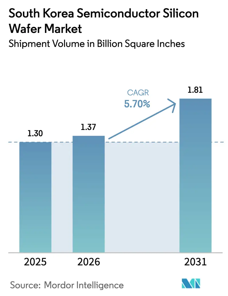
| Base Year Market Size (2025) | 1.30 Billion Square Inches |
| Market Volume (2026) | 1.37 Billion Square Inches |
| Market Volume (2031) | 1.81 Billion Square Inches |
| Growth Rate (2026 - 2031) | 5.70% CAGR |
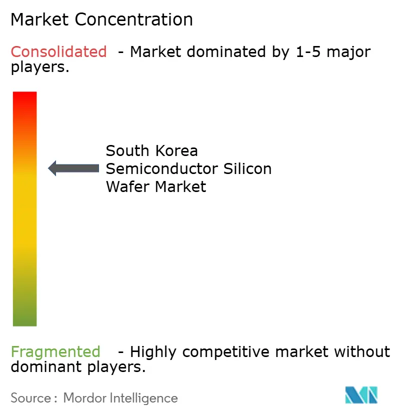
| Market Concentration | Medium |
Major Players *Disclaimer: Major Players sorted in no particular order Image © Mordor Intelligence. Reuse requires attribution under CC BY 4.0. | |
South Korea Semiconductor Silicon Wafer Market Analysis by Mordor Intelligence
The South Korea semiconductor silicon wafer market size was valued at 1.30 billion square inches in 2025 and is estimated to grow from 1.37 billion square inches in 2026 to reach 1.81 billion square inches by 2031, at a CAGR of 5.70% during the forecast period (2026-2031). HBM-driven demand, mega-fab construction, and policy incentives are lifting wafer consumption to structurally higher levels. SK Hynix secured 62% of the global HBM market in 2025, while Samsung qualified HBM4 for NVIDIA’s Rubin platform in early 2026, locking in multi-year orders that pull prime 300 mm supply. Spot DDR5 prices quadrupled between September 2025 and early 2026, signaling structural tightness that supports sustained wafer procurement. Simultaneously, the K-Chips Act expanded tax credits through 2031 and relaxed zoning limits, accelerating fab schedules and amplifying silicon requirements. Rising automotive electrification and SiC-on-silicon hybrids add a new specialty substrate growth vector, although feedstock dependence on Chinese polysilicon and surging electricity costs cap upside potential.
Key Report Takeaways
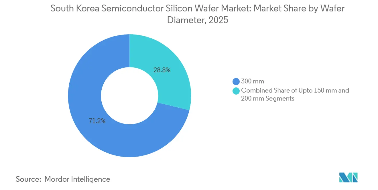
- By wafer diameter, the 300 mm segment held 71.20% of South Korea semiconductor silicon wafer market share in 2025 and is projected to expand at a 6.66% CAGR through 2031.
- By semiconductor device type, logic devices led with 35.41% revenue share in 2025, while memory recorded the fastest forecast CAGR at 6.29% through 2031.
- By wafer type, prime polished wafers commanded 73.32% of the South Korea semiconductor silicon wafer market size in 2025, and silicon-on-insulator substrates are advancing at a 6.58% CAGR to 2031.
- By end-user, consumer electronics accounted for 39.45% of volume in 2025, whereas automotive applications are accelerating at a 6.34% CAGR between 2026-2031.
Note: Market size and forecast figures in this report are generated using Mordor Intelligence’s proprietary estimation framework, updated with the latest available data and insights as of January 2026.
Global valuation is built by aggregating outputs from multiple countries and regions, with South korea being one of the contributors. Our global semiconductor silicon wafer market size represents that cumulative total.
South Korea Semiconductor Silicon Wafer Market Trends and Insights
Drivers Impact Analysis*
| Driver | (~) Impact on CAGR Forecast | Geographic Relevance | Impact Timeline |
|---|---|---|---|
| Intensifying Foundry Investments by Samsung and SK Hynix | +2.1% | National, concentrated in Pyeongtaek, Yongin, Cheongju | Medium term (2-4 years) |
| Government Subsidies for 300 mm Fab Expansion | +1.3% | National, with spillover to regional equipment clusters | Medium term (2-4 years) |
| Shift Toward Advanced Logic Nodes Requiring Ultra-Flat Prime Wafers | +1.0% | National, Pyeongtaek and Hwaseong foundry zones | Short term (≤ 2 years) |
| Growth in Automotive Power Electronics and SiC-on-Silicon Hybrid Demand | +0.8% | National, with early adoption in Bucheon and Gumi | Long term (≥ 4 years) |
| Rising Domestic Demand for Chiplet Interposer Wafers | +0.4% | National, advanced packaging hubs | Medium term (2-4 years) |
| Emergence of Smart-Factory Wafer Reclaim Services | +0.2% | National, industrial automation zones | Long term (≥ 4 years) |
| Source: Mordor Intelligence | |||
Intensifying Foundry Investments By Samsung And SK Hynix
SK Hynix added KRW 21.6 trillion (USD 15.4 billion) to Yongin Phase 1 funding in February 2026, lifting total Phase 1 spend to KRW 31 trillion (USD 22.1 billion) and advancing cleanroom opening to February 2027.[1]Jieun Han, “SK Hynix Adds KRW 21.6 Trillion to Yongin Phase-1 Budget,” yna.co.kr The 4.16 million m² campus plans four high-volume fabs and seeks cumulative outlays of KRW 600 trillion (USD 428.6 billion) through 2050.[2]Se-jong Gab, “600-Trillion-Won Yongin Project to Lift Monthly Wafer Capacity,” sedaily.com Samsung restarted Pyeongtaek Line 5 in late 2025 with more than KRW 60 trillion (USD 42.9 billion) earmarked for HBM4 and 2 nm logic. Combined, these mega-fabs add roughly 200,000 wafers per month by 2030, dwarfing legacy DRAM volumes and compelling suppliers to align multi-year crystal-pulling expansions.
Government Subsidies For 300 mm Fab Expansion
The July 2024 K-Chips Act raised tax credits to 20% for large firms and 30% for SMEs and extended eligibility through 2031. Coupled with the National Advanced Strategic Industry Act, floor-area ratios climbed to 490% and allowable building height to 150 m, enabling SK Hynix to enlarge Yongin cleanrooms by about 1.5 times. Preferential grid connections secured 9 GW of the 15 GW required for first-phase operations. These measures reduce per-wafer capital intensity, guarantee multi-year procurement visibility for wafer makers, and reinforce the South Korea semiconductor silicon wafer market’s investment flywheel.
Shift Toward Advanced Logic Nodes Requiring Ultra-Flat Prime Wafers
Samsung aims for 21,000 wafer-starts-per-month at 2 nm by end-2026, although yields remain under 40%. Low yields inflate wafer consumption per good die, and high-NA EUV tools demand total thickness variation below 0.15 µm, confining qualified supply to Shin-Etsu, SUMCO, and SK Siltron. SK Hynix introduced high-NA EUV at its Icheon M16 facility in September 2025, and Samsung plans deployment at Pyeongtaek Line 5 for 1.4nm development. The shift toward advanced nodes thus favors suppliers capable of delivering ultra-flat prime wafers with minimal edge-exclusion zones, pressuring second-tier vendors to either upgrade their crystal-pulling and polishing equipment or exit the high-end segment, thereby consolidating the supply base around SUMCO, Shin-Etsu, and SK Siltron.
Growth In Automotive Power Electronics And SiC-On-Silicon Hybrid Demand
SK Key Foundry began producing SiC substrates in 1H 2026 to serve electric-vehicle inverters, while onsemi expanded its Bucheon line beyond 1 million wafers per year. Power-SOI adoption widened as automakers embraced 800 V batteries, leveraging SOI’s low switching loss. Although pure SiC wafer supply remains constrained, SiC-on-silicon hybrids provide cost-effective pathways, positioning automotive as the fastest-growing end-user segment at a 6.34% CAGR through 2031. However, the segment's maturity depends on resolving SiC substrate yield challenges and scaling epitaxial deposition capacity, both of which remain bottlenecks in 2026.
Restraints Impact Analysis*
| Restraint | (~) Impact on CAGR Forecast | Geographic Relevance | Impact Timeline |
|---|---|---|---|
| Concentration of Polysilicon Feedstock Imports from China | -0.9% | National, with supply-chain exposure to Xinjiang region | Short term (≤ 2 years) |
| Volatile Electricity Costs Amidst Carbon-Neutral Targets | -0.7% | National, acute in Pyeongtaek and Yongin clusters | Medium term (2-4 years) |
| Technology Gap in 450 mm R&D Funding | -0.3% | National, with limited consortium participation | Long term (≥ 4 years) |
| High Barrier to Entry for Crystal Pulling Equipment Vendors | -0.2% | National, concentrated among incumbent suppliers | Long term (≥ 4 years) |
| Source: Mordor Intelligence | |||
Concentration Of Polysilicon Feedstock Imports From China
China accounted for approximately 80% of global polysilicon production in 2024, with Xinjiang-based producers dominating low-cost supply, while South Korea's domestic output, led by OCI, remained insufficient to meet wafer-grade purity requirements at scale. For South Korean wafer manufacturers, this translates into procurement risk, any disruption to Xinjiang supply would force a shift to higher-cost Japanese or German feedstock, inflating crystal-pulling costs by an estimated 15-20% and eroding gross margins in a market where wafer pricing is largely pass-through. Domestic producer OCI cannot close the gap quickly, and qualification of alternative ultra-pure feedstock exceeds 18 months, tempering short-term wafer output and shaving 0.9 percentage points from forecast CAGR.
Volatile Electricity Costs Amidst Carbon-Neutral Targets
Industrial power tariffs leaped by 75% from 2021-2025, reaching 179.2 won/kWh in 2025. Samsung Electronics' annual electricity bill reached approximately KRW 3.26 trillion (USD 2.3 billion), while SK Hynix's totaled approximately KRW 1.17 trillion (USD 836 million), with wafer fabrication accounting for the majority of consumption.[3]Korea Times Staff, “Semiconductor Firms Face Power Crunch as Electricity Costs Soar,” koreatimes.co.kr The Yongin cluster requires 15 gigawatts at full build-out, yet only 9 gigawatts were secured as of 2025, forcing reliance on diesel generators or grid-extension projects that add KRW 2-3 trillion (USD 1.4-2.1 billion) in infrastructure costs. Elevated energy costs and looming carbon levies could trim market CAGR by 0.7 percentage points through 2031.
*Our forecasts treat driver/restraint impacts as directional, not additive. The impact forecasts reflect baseline growth, mix effects, and variable interactions.
Segment Analysis
By Wafer Diameter: 300 mm Segment Consolidates Advanced-Node Momentum
The 300 mm category captured 71.20% of South Korea semiconductor silicon wafer market share in 2025, reflecting its status as the workhorse for HBM and 2 nm logic. Samsung produced about 8.175 million 300 mm DRAM wafers in 2026, 1.28 times SK Hynix’s 6.39 million, reinforcing scale leadership. HBM4 stacks consume nearly three times the wafer area of DDR5 per gigabyte, so even flat unit shipments translate to rising substrate volumes. SUMCO’s decision to close its 200 mm Miyazaki plant by end-2026 underscores the structural pivot to 300 mm lines.
High-NA EUV deployment cements the 300 mm advantage, as the tooling ecosystem and sub-30 nm nanotopography requirements are matched by only a few suppliers. The South Korea semiconductor silicon wafer market size for sub-150 mm diameters continues to dwindle, limited to niche high-voltage devices. As mega-fabs ramp, logistics and furnace capacity form natural barriers that consolidate the diameter mix around 300 mm for the long term.


By Semiconductor Device Type: Logic Demand Multiplies Throughput
Logic wafers led 2025 volume at 35.41%, fed by Samsung’s KRW 23 trillion (USD 16.4 billion) AI accelerator order book and 2 nm ramp. Yields below 40% elevate wafer starts, magnifying prime substrate pull. Memory remains the largest absolute consumer due to SK Hynix’s 62% HBM share, yet its CAGR trails logic by a fractional margin.
Analog and discrete segments serve automotive, industrial, and power-conversion applications, with growth tied to electrification and renewable-energy inverters. These devices typically use 200mm or smaller wafers, aligning with SUMCO's strategic exit from 200mm production and suggesting a gradual migration toward 300mm for cost efficiency in high-volume analog lines. This convergence elevates blended wafer demand, ensuring that the South Korea semiconductor silicon wafer market continues balancing high-margin advanced nodes with cost-sensitive legacy lines.
By Wafer Type: Prime Polished Anchors Volume While SOI Climbs
Prime polished wafers dominated 73.32% of 2025 shipments, underpinned by DRAM and mainstream logic cycles. However, silicon-on-insulator takes the growth crown with a 6.58% CAGR, driven by RF-SOI in 5G base stations and Power-SOI in electric-vehicle powertrains. Epitaxial wafers, which feature a thin crystalline layer grown atop a bulk substrate, are used in advanced CMOS image sensors and certain power devices, with demand tied to smartphone camera upgrades and automotive LiDAR systems. Specialty silicon, including high-resistivity and sensor-grade substrates, addresses niche markets such as radiation-hard electronics and MEMS accelerometers, commanding premium pricing but limited volumes.
The strategic dynamic lies in the margin differential; prime polished wafers compete largely on cost and delivery reliability, with pricing pressure from volatility in Chinese polysilicon, while SOI and epitaxial substrates capture value through intellectual property in layer-transfer processes and defect engineering. As substrate engineering becomes a differentiation lever, the South Korean semiconductor silicon wafer market linked to SOI grows faster than the overall market.

By End-User: Consumer Devices Dominate As Automotive Surges
Consumer electronics accounted for 39.45% of 2025 demand, driven by AI-enabled smartphones and PCs that incorporate 3 nm application processors and multi-camera modules. Automotive volumes, though smaller, post the strongest growth at 6.34% annually through 2031, the fastest rate among end-user segments. Within consumer electronics, mobile and smartphone demand remained robust despite unit-shipment saturation, as flagship devices integrated advanced application processors on 3nm and 2nm nodes, HBM-equipped AI accelerators for on-device inference, and multi-camera arrays requiring epitaxial wafers for CMOS image sensors.
Industrial and telecommunications segments grow steadily, leveraging analog, sensor, and RF-SOI wafers. Automotive’s ascendancy rebalances substrate portfolios toward SiC hybrids and high-resistivity SOI, broadening supplier mix within the South Korean semiconductor silicon wafer market. The end-user segmentation thus reveals a transition from volume-driven consumer electronics toward value-driven automotive and industrial applications, where substrate specifications, reliability standards, and supply-chain localization increasingly influence procurement decisions and wafer-type mix.
Geography Analysis
South Korean wafer demand is highly clustered. Yongin’s 4.16 million m² complex could attract KRW 600 trillion (USD 428.6 billion) through 2050, anchoring HBM capacity additions that absorb significant 300 mm supply. Pyeongtaek, already at 2.89 million m², saw Samsung restart Line 5 construction in late 2025, signaling further prime wafer pull once the line goes live in 2028. Cheongju’s M15X and Icheon’s high-NA EUV lines tighten concurrent supply needs, stressing just-in-time logistics and elevating inventory buffers.
Infrastructure limitations shadow this concentration. Yongin still needs 6 GW of incremental electricity, while water allocations from the Han River basin face competing industrial claims. Policy adjustments raised zoning caps, improving throughput per plot but magnifying single-site risk for power or water outages. These geographic realities shape the cadence of wafer procurement and reinforce the importance of diversified reclaim and stockpile strategies for fabs.
International linkages remain critical. Imports of Chinese polysilicon and Japanese crystal-pulling tools intersect with exports of finished wafers to Southeast Asian OSAT hubs. U.S. Section 232 probes and new polysilicon tariffs elevate sourcing uncertainty, nudging Korean suppliers to court European and North American feedstock. GlobalWafers’ Texas expansion provides an alternate North American node, yet the South Korea semiconductor silicon wafer market retains a national-centric identity defined by mega-cluster economics and localized ecosystem density.
Coverage of the semiconductor silicon wafer market by Mordor Intelligence spans a wide geographic footprint, with regional analysis available for Europe, North America, and Asia, alongside detailed country-level intelligence for Japan, India, Germany, United States, Taiwan, and China, each shaped by local operating conditions.
Competitive Landscape
SK Siltron, SUMCO, and Shin-Etsu hold the bulk of 300 mm prime capacity, giving the market a moderate concentration profile. SK Siltron entered sale talks with Doosan in 2025 at a KRW 5 trillion (USD 3.6 billion) valuation, while simultaneously budgeting KRW 1.7 trillion (USD 1.2 billion) for a third Gumi 300 mm line in 2026 and KRW 640 million (USD 457 million) for Bay City SiC output, underscoring strategic tension between divestiture and expansion. SUMCO’s shuttering of its Miyazaki 200 mm site by end-2026 illustrates a full-throttle pivot to 300 mm AI wafers.
Specialty niches see Soitec, GlobalWafers, and Siltronic jockey for SOI and epitaxial share. GlobalWafers opened its Texas Phase 1 fab in May 2025 as part of a USD 3.5 billion first tranche, creating optionality for Korean customers hedging geopolitical risk. Siltronic’s Singapore startup in 2024 strengthens regional supply, but capacity additions remain lumpy due to furnace lead times exceeding 18 months.
Emerging opportunities lie in reclaim, chiplet interposers, and SiC hybrids. Reclaim aligns with ESG imperatives yet is underpenetrated in Korea relative to Taiwan and Japan. Chiplet interposer wafers demand ultra-flatness and TSV precision that only a few can deliver at volume, while SiC-on-silicon hybrids marry cost and performance for EV power modules. Capital barriers of USD 10 million per 300 mm furnace and lengthy qualification cycles deter new entrants, locking incumbents into favorable competitive positions within the South Korea semiconductor silicon wafer industry.
South Korea Semiconductor Silicon Wafer Industry Leaders
SK Siltron Co. Ltd.
SUMCO Corporation
Shin-Etsu Handotai Co., Ltd.
GlobalWafers Co., Ltd.
Siltronic AG
- *Disclaimer: Major Players sorted in no particular order

Recent Industry Developments
- February 2026: SK Hynix committed KRW 21.6 trillion (USD 15.4 billion) incremental funding to Yongin Phase 1, advancing cleanroom opening to Feb 2027.
- February 2026: Samsung and SK Hynix both began HBM4 mass production, with Samsung qualifying for NVIDIA Rubin and SK Hynix targeting 12-layer stacks.
- January 2026: Samsung posted preliminary Q4 2025 revenue of KRW 93 trillion (USD 66.4 billion) and operating profit of KRW 20 trillion (USD 14.3 billion) on memory strength.
- November 2025: Samsung resumed Pyeongtaek Line 5 construction, budgeting over KRW 60 trillion (USD 42.9 billion) for HBM4 and logic capacity.
- November 2025: SK Hynix outlined a potential KRW 600 trillion (USD 428.6 billion) long-term plan for the Yongin cluster.


South Korea Semiconductor Silicon Wafer Market Report Scope
The South Korea Semiconductor Silicon Wafer Market refers to the industry focused on the production, distribution, and utilization of silicon wafers used in semiconductor devices.
The South Korea Semiconductor Silicon Wafer Market Report is Segmented by Wafer Diameter (Up to 150mm, 200mm, and 300mm), Semiconductor Device Type (Logic, Memory, Analog, Discrete, and Other), Wafer Type (Prime, Polished, Epitaxial, SOI, and Specialty Silicon), and End-user (Consumer Electronics, Industrial, Telecommunications, Automotive, and Other). The Market Forecasts are Provided in Terms of Volume (Square Inches).
| Up to 150 mm |
| 200 mm |
| 300 mm |
| Logic |
| Memory |
| Analog |
| Discrete |
| Other Semiconductor Device Types |
| Prime |
| Polished |
| Epitaxial |
| Silicon-on-Insulator (SOI) |
| Specialty Silicon (High-Resistivity, Power, Sensor-Grade) |
| Consumer Electronics | Mobile and Smartphones |
| PCs and Servers | |
| Industrial | |
| Telecommunications | |
| Automotive | |
| Other End-user Applications |
| By Wafer Diameter | Up to 150 mm | |
| 200 mm | ||
| 300 mm | ||
| By Semiconductor Device Type | Logic | |
| Memory | ||
| Analog | ||
| Discrete | ||
| Other Semiconductor Device Types | ||
| By Wafer Type | Prime | |
| Polished | ||
| Epitaxial | ||
| Silicon-on-Insulator (SOI) | ||
| Specialty Silicon (High-Resistivity, Power, Sensor-Grade) | ||
| By End-user | Consumer Electronics | Mobile and Smartphones |
| PCs and Servers | ||
| Industrial | ||
| Telecommunications | ||
| Automotive | ||
| Other End-user Applications | ||


Key Questions Answered in the Report
What is the projected volume for the South Korea semiconductor silicon wafer market in 2031?
The market is expected to reach 1.81 billion square inches by 2031.
Which wafer diameter commands the largest share in South Korea?
The 300 mm segment held 71.20% of national volume in 2025 and continues to dominate.
How fast will automotive wafer demand grow through 2031?
Automotive applications are advancing at a 6.34% CAGR, the fastest across all end-user segments.
What policy tools support new fab construction in South Korea?
The K-Chips Act extends tax credits up to 20-30% and the National Advanced Strategic Industry Act relaxes zoning limits, reducing per-wafer capital costs and accelerating buildouts.
Page last updated on:


