LED Epitaxial Wafer Market Size and Share
Market Overview
| Study Period | 2020 - 2031 |
|---|---|
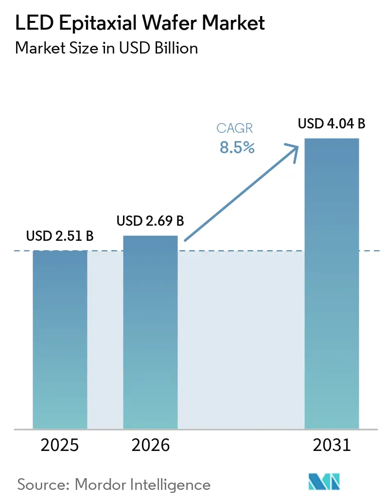
| Market Size (2026) | USD 2.69 Billion |
| Market Size (2031) | USD 4.04 Billion |
| Growth Rate (2026 - 2031) | 8.50% CAGR |
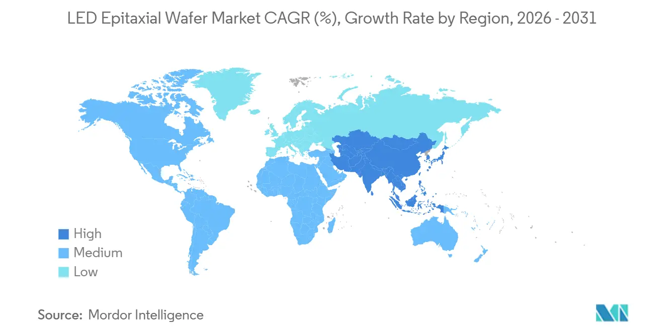
| Fastest Growing Market | Asia Pacific |
| Largest Market | Asia Pacific |
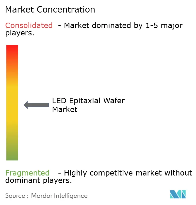
| Market Concentration | Medium |
Major Players *Disclaimer: Major Players sorted in no particular order Image © Mordor Intelligence. Reuse requires attribution under CC BY 4.0. | |
LED Epitaxial Wafer Market Analysis by Mordor Intelligence
The LED epitaxial wafer market size is projected to expand from USD 2.51 billion in 2025 and USD 2.69 billion in 2026 to USD 4.04 billion by 2031, registering an 8.5% CAGR between 2026 and 2031. Sustained shifts toward premium display backlighting, UV-C disinfection, automotive adaptive lighting, and horticultural illumination are replacing volume-driven general-lighting demand. Mini-LED and Micro-LED production lines require wafers with sub-2-nanometer wavelength homogeneity, which raises average selling prices despite competitive pressure. GaN-based products retained the lead in 2025, yet AlGaN substrates are outpacing the baseline as hospitals, food-processing plants, and aircraft cabins deploy mercury-free sterilization fixtures. Silicon substrates are scaling rapidly because 200 millimeter GaN-on-Si delivers 2.3 times more die per run than 150 millimeter sapphire, cutting cost per lumen and tightening binning tolerance for automotive headlamps. Asia-Pacific dominates capacity thanks to subsidy-backed expansions in China, Taiwan, and South Korea, while North American buyers face tariff-driven cost escalations that motivate the reshoring of silicon-based supply chains.
Key Report Takeaways
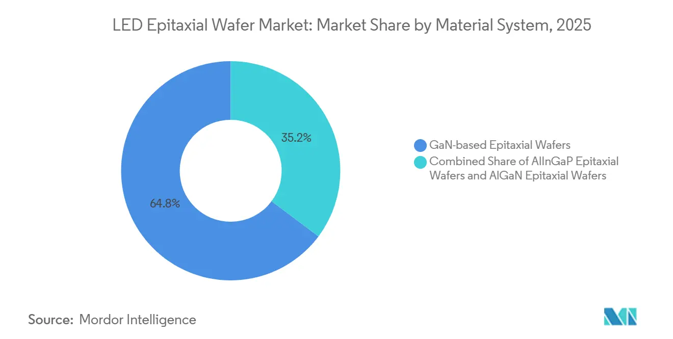
- By material system, GaN-based wafers held 64.8% of the LED epitaxial wafer market share in 2025, while AlGaN is forecast to register an 11.14% CAGR through 2031.
- By substrate, sapphire commanded 57.54% of the LED epitaxial wafer market size in 2025, and silicon is projected to advance at a 12.36% CAGR between 2026 and 2031.
- By wafer diameter, the 150 millimeter format accounted for 43.35% of the LED epitaxial wafer market share in 2025, whereas 200 millimeter and above will grow at a 12.62% CAGR through 2031.
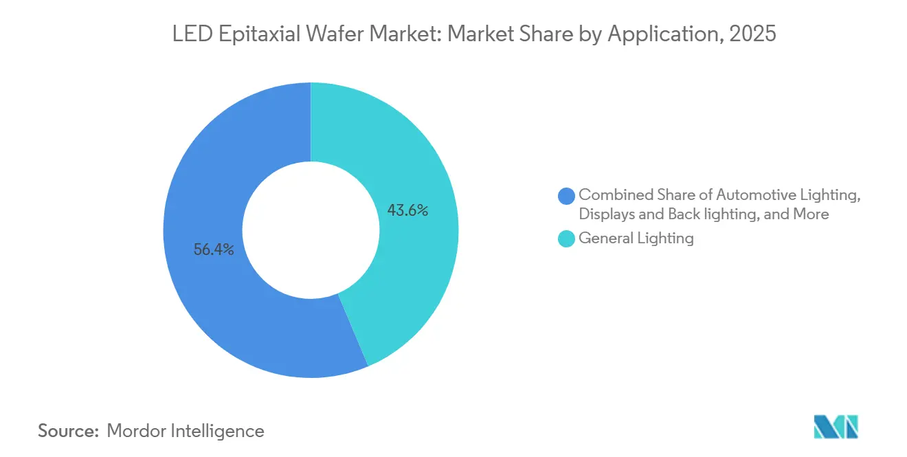
- By application, displays and backlighting are set to post the fastest 14.32% CAGR to 2031, overtaking general lighting, which led with 43.64% revenue share in 2025.
- By geography, Asia-Pacific accounted for 73% of 2025 revenue and is expanding at an 11.35% CAGR through 2031.
Note: Market size and forecast figures in this report are generated using Mordor Intelligence’s proprietary estimation framework, updated with the latest available data and insights as of January 2026.
Global LED Epitaxial Wafer Market Trends and Insights
Drivers Impact Analysis*
| DRIVER | (~) % IMPACT ON CAGR FORECAST | GEOGRAPHIC RELEVANCE | IMPACT TIMELINE |
|---|---|---|---|
| Proliferation of Mini and Micro-LED Display Manufacturing | +2.1% | Asia-Pacific core, spill-over to North America | Medium term (2–4 years) |
| Government Energy-Efficiency Regulations Phasing Out Incandescent Lighting | +1.8% | Global, accelerated in EU and North America | Long term (≥ 4 years) |
| Rapid Adoption of UV-C LED Diodes for Disinfection Post-COVID-19 | +1.5% | North America and Europe, expanding to Asia-Pacific | Short term (≤ 2 years) |
| Automotive Headlamp Migration to Matrix LED and ADB Systems | +1.3% | Europe and North America, gradual in Asia-Pacific | Medium term (2–4 years) |
| Surge in Demand for Horticultural Lighting in Controlled-Environment Agriculture | +0.9% | North America and Europe, emerging Middle East farms | Medium term (2–4 years) |
| Expansion of GaN-on-Si Technology Lowering Cost per Lumen | +0.9% | Global, led by Asia-Pacific hubs | Long term (≥ 4 years) |
| Source: Mordor Intelligence | |||
Proliferation of Mini and Micro-LED Display Manufacturing
Panel makers are fast-tracking Mini-LED backlighting and direct-view Micro-LED projects, which depend on wafers with extremely tight wavelength binning to reduce color shift across thousands of sub-pixels. TCL CSOT’s 80% stake in Prima secures 6,000 square-meter monthly wafer supply for 10,000-nit video walls, while AUO’s 4.5-generation line has locked 114-inch television orders from Samsung and in-vehicle panels for Sony Mobility.[1] Infineon’s 300 millimeter GaN sample run delivered 2.3 times more chips per wafer, illustrating how scale economics are converging with display-grade uniformity targets.[2]
Government Energy-Efficiency Regulations Phasing Out Incandescent Lighting
The United States Department of Energy finalized a 120 lumens-per-watt mandate that takes effect in July 2028, effectively prohibiting incandescent and halogen bulbs. Parallel bans on compact fluorescents in ten U.S. states and strict lumen-maintenance rules under IEC 62717 are pushing fixture OEMs toward high-efficacy LED modules, boosting demand for defect-free GaN wafers. China’s subsidy program rewards >130 lumens-per-watt lamps, steering domestic makers toward large-diameter GaN-on-Si lines that minimize material cost.
Rapid Adoption of UV-C LED Diodes for Disinfection Post-COVID-19
FDA De Novo clearance for HAI Solutions’ QIKCAP in January 2026 and 510(k) approval for Surfacide’s Helios+ in June 2025 established clinical benchmarks for UV-C arrays based on AlGaN wafers operating at 260-280 nanometers.[4]United States Food and Drug Administration, “Recently Approved Devices,” fda.gov Hospitals, water utilities, and HVAC OEMs are converting from mercury-vapor lamps to solid-state emitters that switch instantly, eliminate hazardous disposal, and fit compact footprints. Device integrators now specify aluminum mole fractions above 30%, which intensifies crystalline-quality requirements and elevates wafer ASPs.
Automotive Headlamp Migration to Matrix LED and ADB Systems
NHTSA’s 2024 rejection of requests to relax photometric rules keeps stringent candela thresholds in place, compelling automakers to invest in finely binned GaN wafers for adaptive driving beams.[5]National Highway Traffic Safety Administration, “Adaptive Driving Beam Headlamps Approval,” nhtsa.govMatrix LED headlamps integrate up to 100 addressable segments per module, each driven at 1,000-1,500 lumens, while early Micro-LED prototypes promise pixel-level resolution for roadway projection. Seoul Semiconductor’s wire-bond-free WICOP package enhances thermal dissipation, sustaining high drive currents in compact automotive optics.
Restraints Impact Analysis*
| RESTRAINT | (~) % IMPACT ON CAGR FORECAST | GEOGRAPHIC RELEVANCE | IMPACT TIMELINE |
|---|---|---|---|
| High Capital Expenditure for MOCVD Reactors and Epitaxy Tools | -1.2% | Global, most acute North America and Europe | Long term (≥ 4 years) |
| Yield Challenges for Larger (200 mm) GaN Wafers | -0.9% | Global, concentrated Asia-Pacific hubs | Medium term (2–4 years) |
| Supply Chain Dependence on Limited Sapphire Substrate Suppliers | -0.7% | Global, heightened Asia-Pacific risk | Short term (≤ 2 years) |
| Intense Price Erosion Squeezing Mid-Tier Manufacturers | -0.6% | Asia-Pacific core, spill-over globally | Short term (≤ 2 years) |
| Source: Mordor Intelligence | |||
High Capital Expenditure for MOCVD Reactors and Epitaxy Tools
A modern 200 millimeter GaN MOCVD chamber costs upward of USD 3 million, and a viable line requires at least ten chambers, lifting entry barriers for new ventures. Veeco Instruments booked fresh Lumina orders in March 2026 that highlight the constant need for next-generation epitaxy hardware, yet the 12-18 month re-qualification cycle postpones payback, especially in Europe and the United States, where labor and compliance inflate project budget. Smaller firms, therefore, gravitate toward niche wavelengths or license capacity from over-built Chinese fabs.
Yield Challenges for Larger (200 mm) GaN Wafers
Bow-induced stress on 200 millimeter GaN-on-sapphire or GaN-on-Si reduces usable die yield to as low as 70% for high-brightness applications, compared with 90% for 150 millimeter formats. Infineon’s 300 millimeter pilot lot underscored that further buffer-layer innovation is needed to suppress threading-dislocation densities before true cost advantages materialize. UV-C AlGaN wafers suffer even greater mismatch, keeping most production on 100 millimeter lines and constraining economies of scale.
*Our forecasts treat driver/restraint impacts as directional, not additive. The impact forecasts reflect baseline growth, mix effects, and variable interactions.
Segment Analysis
By Material System: AlGaN Captures UV-C Momentum
GaN-based wafers captured 64.8% of the 2025 value, underpinned by blue emission for phosphor-converted white lamps, RGB backlights, and automotive headlamps. AlGaN accounted for a modest portion of the LED epitaxial wafer market size in 2025, yet its 11.14% CAGR through 2031 outpaces the sector as hospitals and utilities mandate mercury-free sterilization technologies. FDA clearances for HAI Solutions, Surfacide, and UV Smart devices set performance bars that only tight-bandgap AlGaN can meet. GaN still delivers the lowest cost per lumen for general illumination and Mini-LED backlights, protecting a 70% revenue share. AlInGaP maintains relevance in automotive signaling and outdoor signage, but faces gradual substitution by phosphor-converted alternatives that streamline inventory.
AlGaN wafers require aluminum fractions exceeding 30%, which exacerbates lattice mismatch and lowers quantum efficiency to 3-5 milliwatts per chip, obligating integrators to design multi-chip arrays. GaN suppliers counter with process maturity and a vast installed base of MOCVD systems, enabling aggressive price moves that defend share. Seoul Semiconductor’s patent-rich WICOP platform uses GaN chips without wire bonds, improving thermal paths for automotive Mini-LED clusters. AlInGaP’s future rests on specialized far-red horticultural fixtures and light-based communication modules where direct red output avoids Stokes losses.


By Substrate Type: Silicon Gains on Cost
Sapphire retained 57.54% of 2025 revenue thanks to crystalline quality and established polishing routes, yet silicon is closing the gap as 200 millimeter GaN-on-Si slices deliver 2.3 times more die per run, slashing cost per lumen. Section 301 tariffs that doubled wafer duties to 50% in 2025 nudged North American integrators toward local silicon suppliers, accelerating adoption. Silicon-based GaN is the natural challenger, offering a larger 200 mm diameter, lower raw-wafer cost, and compatibility with existing CMOS fabs, underpinning a 12.36% CAGR that overtakes sapphire growth. Silicon carbide earns premium demand in high-power projectors and medical scopes where extreme current densities warrant its superior thermal conductivity, despite USD 500-1,000 wafer prices.
GaN-on-Si experiences bow challenges that hit yields, but design margins in commodity bulbs tolerate 70% die utilization. Sapphire excels in automotive and outdoor luminaires that endure harsh thermal cycling. Silicon carbide remains a niche yet vital option for mission-critical applications. Gallium arsenide volumes are declining as AlInGaP-on-GaAs migrates to GaN platforms, aligning multi-color modules on a common substrate to simplify package integration.
By Wafer Diameter: 200 mm Scales Economics
The 150 millimeter format controlled 43.35% of 2025 revenue, reflecting legacy reactor fleets, yet 200 millimeter lines are forecast to deliver a 12.62% CAGR to 2031. Infineon’s 300 millimeter proof-of-concept demonstrates the longer-term roadmap, although beyond 50 micrometers still complicates lithography alignment. AUO’s 4.5-generation Micro-LED fab highlights how larger substrates are essential for mass-transfer yield models tied to enormous pixel counts.
Transitioning an existing reactor from 150 millimeters to 200 millimeters takes up to 18 months, freezing cash flow and deterring mid-tier players during ASP downturns. Yet automotive OEMs are pressuring suppliers for tighter binning that only larger wafers can consistently provide. Up to 100 millimeter sizes persist in deep-UV runs where stress management trumps economies of scale. Equipment vendors are standardizing 200 millimeter handling tools adapted from silicon IC fabs, which lowers ancillary capital outlays by 15%-20 percent compared with bespoke 150 millimeter gear.
By Application: Displays Outpace Lighting
General lighting retained 43.64% share in 2025, underpinned by retrofit programs triggered by incandescent bans, but displays and backlighting will post the fastest 14.32% CAGR as consumer electronics brands release Mini-LED tablets and Micro-LED televisions. TCL CSOT’s Suzhou line delivers 10,000-nit panels that rely on wafer-level wavelength uniformity tighter than ±1 nanometer. Automotive lighting is shifting to matrix beams with 20-100 addressable segments, and early Micro-LED prototypes promise enhanced resolution for future adaptive driving systems.
UV sterilization demand is expanding in hospitals, aircraft cabins, and HVAC systems where rapid log-6 pathogen reduction is mandatory, lifting AlGaN shipments. Horticultural operators in vertical farms and greenhouses are specifying multispectral arrays that extend photoperiods and tailor red-to-blue ratios for higher yields. Industrial and specialty fixtures span machine-vision illuminators and signal beacons that require narrow band gaps, supporting bespoke wafer runs with premium margins.
Geography Analysis
Asia-Pacific generated 73% of the LED epitaxial wafer market revenue in 2025 and will maintain an 11.35% CAGR through 2031 as Chinese, Taiwanese, and South Korean clusters scale MOCVD fleets under subsidy programs. China’s Ministry of Industry and Information Technology offers rebates for lamps above 130 lumens per watt, hastening the transfer from sapphire to GaN-on-Si to trim material cost. Taiwan’s Epistar and Lextar anchor an integrated hub that pairs wafer growth with downstream packaging and Mini-LED panel assembly. South Korea’s Samsung and LG Innotek channel investment into Micro-LED pilot lines tied to next-generation televisions and automotive displays.
North America accounts for a modest share yet captures outsized value on premium pricing for aerospace, defense, and medical devices. Section 301 tariffs that took effect in January 2025 doubled wafer import duties, prompting integrators to source domestic silicon slices or negotiate long-term sapphire contracts to hedge volatility. The United States Department of Energy’s looming 2028 efficacy mandate ensures a continued replacement cycle in residential and commercial fixtures, keeping demand for high-efficiency GaN wafers resilient.
Europe follows a similar path as the EU completes its halogen phase-out while championing connected lighting under Ecodesign directives. German and French automakers front-load orders for matrix headlamps that need defect-free wafers to satisfy ECE beam patterns. Rest of the World, led by Middle East vertical farms, South American water utilities, and African off-grid solar installations, remains a nascent but promising frontier where cost sensitivity favors GaN-on-Si substrates and small-diameter AlGaN wafers tailored to regional climate constraints.

Competitive Landscape
Market concentration is moderate, with the top five suppliers controlling roughly 55% of installed capacity, yet pervasive Chinese expansions suppress average selling prices. Seoul Semiconductor booked KRW 1.932 trillion (USD 1.45 billion) revenue in 2024 and shifted to profit by focusing on wire-bond-free WICOP chips for automotive Mini-LED clusters [SEOULSEMICON.COM]. TCL CSOT’s purchase of Prima in December 2025 secures upstream feedstock and exemplifies a broader wave of vertical integration among panel makers seeking tighter control over wafer parameters.
The strategic landscape is bifurcating. Volume segments favor GaN-on-Si on 200 millimeter platforms that compress cost per lumen, while high-end niches prize GaN-on-sapphire or AlGaN formats for superior quantum efficiency and spectral precision. Emerging disruptors such as Aledia and Plessey develop nanowire and monolithic Micro-LED architectures that could bypass mass-transfer bottlenecks and redistribute profit pools if commercial yields stabilize. Intellectual-property litigation is intensifying, as shown by Seoul Semiconductor’s recent victory at the Unified Patent Court, underlining the role of patents in defending specialty margins.
Strategic moves hinge on capacity rationalization, selective specialization, and technology hedging. Mid-tier Taiwanese and Japanese suppliers unable to fund 200 millimeter upgrades are partnering with equipment makers to co-develop lower-capex MOCVD modules or pivoting to UV-C where smaller wafers suffice. Chinese leaders, buffered by subsidies, pursue pricing offensives that squeeze global peers, yet face their own margin risks as domestic capacity already exceeds internal demand. Western startups target differentiated IP niches, securing venture backing from automotive and consumer electronics OEMs eager for next-generation Micro-LED breakthroughs.
LED Epitaxial Wafer Industry Leaders
Nichia Corporation
Osram Opto Semiconductors GmbH
San'an Optoelectronics Co., Ltd.
Seoul Semiconductor Co., Ltd.
Ennostar Corporation
- *Disclaimer: Major Players sorted in no particular order

Recent Industry Developments
- March 2026: Veeco Instruments received orders for Lumina MOCVD systems aimed at InP and GaN expansions, confirming sustained investment in large-diameter epitaxy tools.
- February 2026: UV Smart secured FDA 510(k) clearance for its D60 probe disinfection device, validating the efficacy of AlGaN wafers in clinical settings.
- January 2026: FDA granted De Novo clearance to HAI Solutions’ QIKCAP UV-C LED platform, the first fully authorized solid-state room-air sterilizer in the United States.
- December 2025: TCL CSOT finalized its 80% acquisition of Prima for CNY 490 million (USD 70 million), securing wafer supply for its Suzhou Mini-LED line.


Global LED Epitaxial Wafer Market Report Scope
The LED Epitaxial Wafer Market Report is segmented by Material System (GaN-based Epitaxial Wafers, AlInGaP Epitaxial Wafers, and AlGaN Epitaxial Wafers), Substrate Type (Sapphire, Silicon, Silicon Carbide (SiC), and Gallium Arsenide (GaAs)), Wafer Diameter (Up to 100 mm, 150 mm, and 200 mm and Above), Application (General Lighting, Automotive Lighting, Displays and Backlighting, UV Sterilization, and Industrial and Specialty Lighting), and Geography (North America, Europe, Asia-Pacific, and Rest of the World). The Market Forecasts are Provided in Terms of Value (USD).
| GaN-based Epitaxial Wafers |
| AlInGaP Epitaxial Wafers |
| AlGaN Epitaxial Wafers |
| Sapphire |
| Silicon |
| Silicon Carbide (SiC) |
| Gallium Arsenide (GaAs) |
| Upto 100 mm |
| 150 mm |
| 200 mm and Above |
| General Lighting |
| Automotive Lighting |
| Displays and Backlighting |
| UV Sterilization |
| Industrial and Specialty Lighting |
| North America |
| Europe |
| Asia-Pacific |
| Rest of the World |
| By Material System | GaN-based Epitaxial Wafers |
| AlInGaP Epitaxial Wafers | |
| AlGaN Epitaxial Wafers | |
| By Substrate Type | Sapphire |
| Silicon | |
| Silicon Carbide (SiC) | |
| Gallium Arsenide (GaAs) | |
| By Wafer Diameter | Upto 100 mm |
| 150 mm | |
| 200 mm and Above | |
| By Application | General Lighting |
| Automotive Lighting | |
| Displays and Backlighting | |
| UV Sterilization | |
| Industrial and Specialty Lighting | |
| By Geography | North America |
| Europe | |
| Asia-Pacific | |
| Rest of the World |


Key Questions Answered in the Report
What is the current size and projected growth of the LED epitaxial wafer market?
The LED epitaxial wafer market size is set to rise from USD 2.69 billion in 2026 to USD 4.04 billion by 2031 at an 8.5% CAGR.
Which material system is expanding fastest?
AlGaN wafers are advancing at an 11.14% CAGR through 2031 due to rising UV-C disinfection demand.
How are tariffs influencing North American sourcing strategies?
Section 301 duties that doubled wafer import tariffs to 50% in 2025 are accelerating the shift toward domestically sourced silicon substrates.
Why are 200 millimeter wafers gaining traction?
They deliver 2.3 times more die per run than 150 millimeter formats, reducing cost per lumen and improving binning uniformity essential for Mini-LED and automotive applications.
What is the chief capital barrier for new entrants?
A full 200 millimeter GaN MOCVD line costs more than USD 30 million in reactor hardware alone, prolonging payback and limiting entry to well-financed players.
Page last updated on:


