China Semiconductor Silicon Wafer Market Size and Share
Market Overview
| Study Period | 2020 - 2031 |
|---|---|
| Forecast Data Period | 2026 - 2031 |
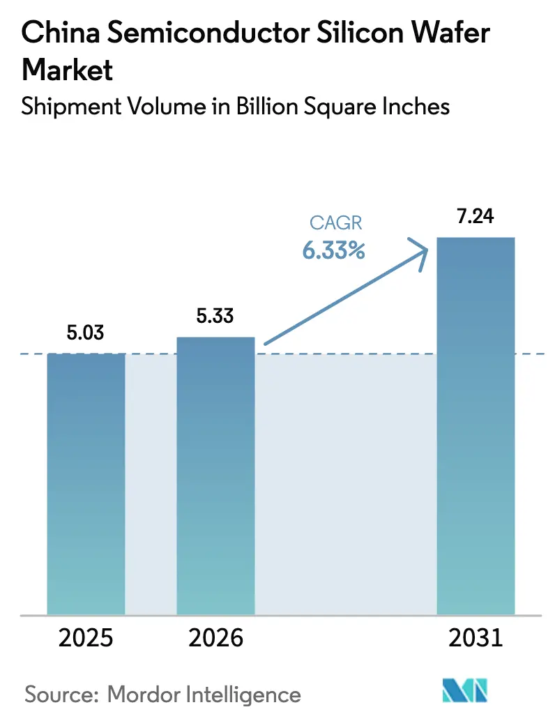
| Base Year Market Size (2025) | 5.03 Billion Square Inches |
| Market Volume (2026) | 5.33 Billion Square Inches |
| Market Volume (2031) | 7.24 Billion Square Inches |
| Growth Rate (2026 - 2031) | 6.33% CAGR |
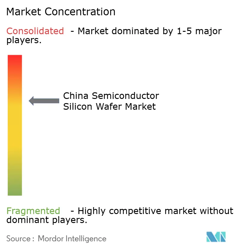
| Market Concentration | Medium |
Major Players *Disclaimer: Major Players sorted in no particular order Image © Mordor Intelligence. Reuse requires attribution under CC BY 4.0. | |
China Semiconductor Silicon Wafer Market Analysis by Mordor Intelligence
The China Semiconductor Silicon Wafer Market size in terms of shipment volume is expected to grow from 5.03 Billion Square Inches in 2025 to 5.33 Billion Square Inches in 2026 and is forecast to reach 7.24 Billion Square Inches by 2031 at 6.33% CAGR over 2026-2031. Robust government funding, tighter export controls on advanced foreign tools, and accelerating capacity additions by local foundries continue to propel demand. Beijing’s 50%-domestic-equipment mandate, in force since early 2026, ties subsidies to the use of home-grown process tools, channeling incremental wafer orders toward Chinese suppliers. Rapid adoption of twelve-inch lines for logic and advanced analog devices, combined with rising electric-vehicle penetration, further elevates total substrate consumption. The market also benefits from surging chiplet-based AI accelerators that require ultra-flat prime wafers to enable hybrid bonding, even as lingering defect-density gaps versus Japanese incumbents keep high-end logic output partially import-dependent.
Key Report Takeaways
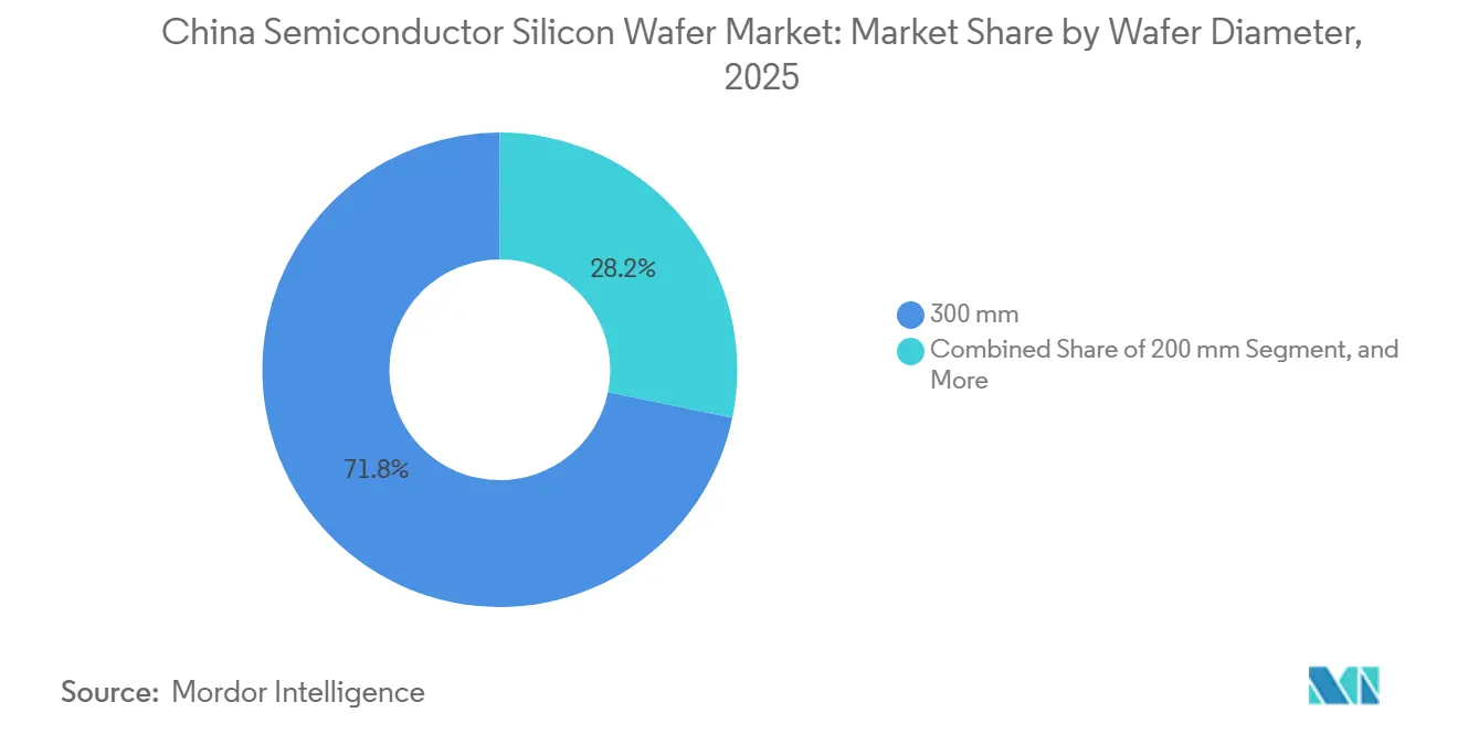
- By wafer diameter, 300 millimeter substrates led with 71.75% of the China semiconductor silicon wafer market share in 2025 and are projected to expand at a 7.16% CAGR through 2031.
- By semiconductor device type, the logic segment captured 33.37% of the China semiconductor silicon wafer market in 2025 and is poised to grow at a 6.82% CAGR through 2031.
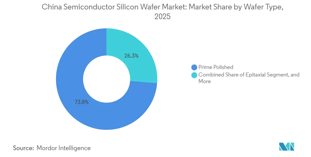
- By wafer type, prime polished wafers commanded 73.75% share of the China semiconductor silicon wafer market size in 2025, while silicon-on-insulator substrates are forecast to grow at a 6.93% CAGR to 2031.
- By end-user, consumer electronics held 40.83% of the China semiconductor silicon wafer market share in 2025, whereas automotive applications are projected to record a 7.01% CAGR through 2031.
Note: Market size and forecast figures in this report are generated using Mordor Intelligence’s proprietary estimation framework, updated with the latest available data and insights as of January 2026.
China holds a defined position within a broader international distribution. The semiconductor silicon wafer market share data by Mordor Intelligence maps that allocation across all contributing countries and regions, globally.
China Semiconductor Silicon Wafer Market Trends and Insights
Drivers Impact Analysis*
| Driver | (~) % Impact on CAGR Forecast | Geographic Relevance | Impact Timeline |
|---|---|---|---|
| Surge in 300mm capacity build-outs by domestic players | +1.8% | National, concentrated in Yangtze River Delta and Beijing-Tianjin corridor | Medium term (2-4 years) |
| Government "50% domestic tool" mandate accelerating local wafer demand | +1.5% | National, with spillover to provincial fab clusters | Short term (≤ 2 years) |
| Automotive SiC power device boom driving 200mm and 8-inch SiC wafer needs | +1.2% | National, early gains in Guangdong, Shanghai, Jiangsu | Medium term (2-4 years) |
| Tight global 200mm tool supply forcing Chinese fabs to lock-in local wafer supply | +0.9% | Global, acute in China due to export restrictions | Short term (≤ 2 years) |
| Subsidized polysilicon price support enhancing cost advantage | +0.7% | National, benefiting integrated wafer producers | Long term (≥ 4 years) |
| Rise of advanced packaging (chiplet / X-DFOI) lifting demand for ultra-flat prime wafers | +0.6% | National, led by JCET, Huawei HiSilicon ecosystem | Medium term (2-4 years) |
| Source: Mordor Intelligence | |||
Surge in 300 mm Capacity Build-Outs by Domestic Players
Semiconductor Manufacturing International Corporation confirmed late-2025 plans to add 40,000 twelve-inch wafer starts each month across Shanghai, Beijing, and Shenzhen fabs by end-2026, a move mirrored by Hua Hong Semiconductor’s additional 20,000-wspm program targeting power-management ICs.[1]Nikkei Staff, “China's SMIC to Add 40,000 Wafer Starts Per Month in 2026,” Nikkei Asia, asia.nikkei.com Provincial incentives in land, taxes, and low-interest loans reduce upfront risk, allowing suppliers to sign multiyear take-or-pay contracts before capacity comes online. Shanghai Silicon Industry Group responded by scaling its Lingang plant to 2 million twelve-inch wafers a month for 2026 delivery. Scale economics below USD 50 per prime wafer become the tipping point, spurring a consolidation wave among smaller startups that cannot reach cost parity with these leaders.
Government “50% Domestic Tool” Mandate Accelerating Local Wafer Demand
Effective January 2026, the Ministry of Industry and Information Technology links subsidies to a minimum 50% local-tool adoption, ratcheting the threshold to 70% by 2028 and full localization in 2030. Foundries that fall short face subsidy claw-backs, so most streamline vendor lists to all-Chinese tool-and-wafer pairings. Naura Technology documented that over 60% of its deposition tools installed on 28 nm lines were matched with Shanghai Silicon substrates, trimming yield-ramp cycles by almost a quarter.[2]Naura Technology, “Annual Report 2025,” naura.com Joint process-recipe sharing inside these closed loops accelerates progress on defect control and flattens the learning curve for new fabs.
Automotive SiC Power Device Boom Driving 200 mm and 8-Inch SiC Wafer Needs
Electric-vehicle sales jumped to 10.8 million units in 2024, and the share equipped with silicon-carbide power modules will climb toward 30% by 2027. BYD Semiconductor’s Changsha fab already runs 10,000 eight-inch SiC wafers per month and targets a 2X expansion for late 2026. NIO and XPeng have secured multiyear supply agreements to secure 200 mm substrates for their 800-volt inverter modules. Although usable die-per-wafer yields trail silicon norms, the performance uplift in charging speed and efficiency offsets the cost premium, ensuring steady demand for SiC substrates even during broader wafer price erosion.
Rise of Advanced Packaging (Chiplet / X-DFOI) Lifting Demand for Ultra-Flat Prime Wafers
Huawei’s Ascend 910C AI accelerator employs a 2.5-D chiplet design bonded to high-bandwidth memory stacks via a silicon interposer, with total-thickness variation kept within 0.3 µm.[3]Huawei Technologies, “Ascend 910C Architecture Details,” huawei.com Jiangsu Changjiang Electronics Technology recorded 35% growth in advanced-packaging revenue in 2025, attributing it to fan-out wafer-level and TSV lines that require ultra-flat substrates. Shanghai Silicon invested USD 120 million in an Ebara CMP line targeting 0.2 µm TV to service these programs. Mastery of planar-flatness specs will let domestic suppliers retain pricing power even as commodity prime-wafer average selling prices fall.
Restraints Impact Analysis*
| Restraint | (~) % Impact on CAGR Forecast | Geographic Relevance | Impact Timeline |
|---|---|---|---|
| Persistent defect-density gap vs. Japanese suppliers in above 28nm logic wafers | -0.8% | National, affecting leading-edge fabs | Medium term (2-4 years) |
| U.S.-led export controls limiting access to critical CZ crystal and CMP tools | -1.2% | National, acute for sub-28nm capacity | Long term (≥ 4 years) |
| Margin pressure from mature-node over-capacity and price-war among foundries | -0.6% | National, concentrated in Yangtze River Delta | Short term (≤ 2 years) |
| Skills shortage in ultra-pure water and chemical waste treatment operations | -0.4% | National, severe in tier-2 cities | Medium term (2-4 years) |
| Source: Mordor Intelligence | |||
Persistent Defect-Density Gap Vs. Japanese Suppliers in above 28 nm Logic Wafers
Average defect density of 0.12 defects cm⁻² on domestic 300 mm prime wafers remains 50% above Shin-Etsu’s 0.08 defects cm⁻² benchmark, translating into roughly 8-10% lower yield for advanced mobile processors. Trace-metal contamination above 0.1 ppb in locally sourced polysilicon is a major contributor. Foundries compensate by implementing longer anneals and tighter incoming inspections, adding USD 15-20 per wafer in costs. High-volume fabless customers, therefore, stipulate Japanese substrates for leading-edge lots, capping the market ceiling for domestic suppliers despite capacity growth.
U.S.-Led Export Controls Limiting Access to Critical CZ Crystal and CMP Tools
The December 2024 Bureau of Industry and Security rule black-listed crystal pullers delivering resistivity uniformity below 5% and sub-28 nm CMP gear, forcing Chinese producers to lean on 2015-2018-vintage machinery. TCL Zhonghuan’s attempted reverse-engineering of an Applied Materials Reflexion platform stalled on software-license barriers, delaying its next-gen wafer line by 18 months. Persistent equipment gaps keep domestic suppliers one to two generations behind, perpetuating reliance on imports for critical substrates.
*Our forecasts treat driver/restraint impacts as directional, not additive. The impact forecasts reflect baseline growth, mix effects, and variable interactions.
Segment Analysis
By Wafer Diameter: Dominance of 300 mm Substrates Underpins Volume Expansion
The 300 mm category accounted for 71.75% of total volume in 2025, capturing the largest slice of the China semiconductor silicon wafer market share and sustaining a 7.16% CAGR through 2031. Capacity additions of 40,000 twelve-inch wafers per month at Semiconductor Manufacturing International Corporation alone underscore an irreversible pivot toward larger-diameter economics, where each 300 mm substrate yields roughly 2.5 times as many die as a 200 mm equivalent for mainstream logic layouts. Cost-per-die savings flow directly into competitive chip pricing, a survival imperative as smartphone and PC refresh cycles extend.
The 200 mm segment remains essential for analog and silicon-carbide devices; global shortages of 200 mm process tools have elevated lead times to 24 weeks, locking automotive customers into multiyear wafer agreements. Sub-150-mm wafers address legacy powertrain and industrial controllers, but face sunset as requalification to larger diameters becomes unavoidable. Nevertheless, the China semiconductor silicon wafer market continues to allocate niche budget to six-inch and eight-inch lines supporting SiC power modules, insulating this pocket from the price erosion afflicting bulk 300 mm primes.


By Semiconductor Device Type: Logic Wafers Remain Core Growth Engine
Logic wafers held 33.37% of 2025 volume, reflecting dominance in AI accelerators, edge processors, and mainstream SoCs. The segment’s 6.82% CAGR to 2031 outpaces memory and analog, helped by domestic AI cloud build-outs that each consume thousands of high-end processors per rack. The China semiconductor silicon wafer market size allocated to logic applications therefore widens, even though some leading-edge die continue to import Japanese substrates for yield security.
Memory wafers trail because domestic DRAM and NAND capacity is still small, whereas discrete power devices, chiefly SiC MOSFETs, post high-single-digit growth off a low base. Analog growth comes from battery-management ICs and automotive sensing, but logic remains the strategic focus as Beijing presses compute sovereignty. Diversified demand also shields logic wafer offtake from cyclical swings in a single end-market, reinforcing its anchor status within overall consumption.
By Wafer Type: Prime Polished Substrates Maintain Scale Advantage
Prime polished wafers contributed 73.75% of total shipments in 2025, underscoring their role as the mainstream workhorse for CMOS. Epitaxial variants, vital for power devices, expand steadily in tandem with vehicle electrification but do not match the absolute scale of prime. Silicon-on-insulator volumes, while modest, are growing at a 6.93% CAGR, driven by RF front-end modules in 5G smartphones and low-power IoT processors.
Specialty silicon, including high-resistivity and power-grade substrates, services RF-switch and IGBT niches that national policies increasingly favor for self-sufficiency. As Chinese epitaxial tool vendors refine uniformity and layer thickness, domestic fabs prefer to bundle wafer procurement with local tool sets to meet the 50% mandate, giving home-grown suppliers an embedded sales advantage across all wafer-type segments of the China semiconductor silicon wafer market.
By End-User: Consumer Electronics Leads, Automotive Provides Fastest Upside
In 2025, consumer electronics accounted for 40.83% of total shipments, underscoring China's dominance as the globe's leading hub for smartphone and PC manufacturing. This dominance is driven by the country's robust supply chain infrastructure and its ability to scale production efficiently. Regular model updates from brands like Xiaomi, Oppo, and Vivo maintain steady wafer run rates, ensuring consistent production levels. Additionally, there's an added boost from server demand linked to AI training clusters, which are increasingly critical for supporting advancements in artificial intelligence technologies.
Automotive-oriented demand, which accounted for only 10% in 2025, is expected to grow at a 7.01% CAGR as semiconductor content per electric vehicle inches toward USD 1,000 by 2027. Each traction inverter, onboard charger, and ADAS module pulls incremental logic, analog, and discrete die, magnifying the wafer needs. Industrial and telecom remain stable in the mid-teens, but vehicle electrification is the standout accelerator for the China semiconductor silicon wafer market.
Geography Analysis
The Yangtze River Delta, covering Shanghai, Jiangsu, and Zhejiang provinces, commanded about 60% of the China semiconductor silicon wafer market share in 2025 and remains the anchor region for new twelve-inch investments. High-capacity sites in Lingang, Kunshan, and Wuxi benefit from concentrated talent, reliable ultra-pure water networks, and express-lane customs that shorten import cycles for specialty gases. Provincial incentives allow foundries to tap land and power at discounted rates, reinforcing the region’s cost advantage even as nationwide wage pressures rise. Robust logistics links to handset and server assembly plants in Suzhou and Shenzhen further lock in wafer demand, ensuring the cluster maintains priority access to incremental substrate supply.
Roughly 20% of capacity is along the Beijing-Tianjin corridor, where the policy focus is on strategic autonomy for compute and defense electronics. Local governments bundle tax holidays with expedited environmental approvals, allowing new fabs to break ground within 6 months of the announcement. Close physical proximity between deposition-tool vendors and wafer makers accelerates joint recipe tuning, shaving weeks off ramp schedules and lowering defect-density drift for 28 nm logic lines. The corridor’s strong university pipeline feeds process-engineering talent into both equipment and wafer plants, aligning workforce development with the compound annual growth goals of the broader industry.
Emerging hubs in Guangdong, Sichuan, Hunan, and Anhui jointly account for the remaining 20% of installed capacity but generate a disproportionate share of specialty wafer innovation. Changsha’s eight-inch SiC lines serve the fast-growing electric-vehicle ecosystem, while Chengdu and Chongqing fabs focus on power discretes and high-resistivity substrates. Although each site is smaller than its counterparts on the coast, aggressive provincial subsidies for tooling and clean-room build-outs allow them to scale quickly; collectively, they are expected to add more than 800,000 twelve-inch wafer equivalents by 2031, expanding the China semiconductor silicon wafer market beyond the historical coastal footprint. Geographic diversification also distributes utility-supply risk, shielding national output from localized power or water disruptions.
Mordor Intelligence delivers a comprehensive view of the semiconductor silicon wafer market across all major regions such as Europe, North America, and Asia, alongside country-level analysis for Taiwan, Japan, Germany, United States, South Korea, and India, each offering a view of the local market realities.
Competitive Landscape
Domestic suppliers remain in a transitional phase, with Shanghai Silicon Industry Group, TCL Zhonghuan, and National Silicon Industry Group together holding close to 35% of 300 mm prime shipments, while Japanese leaders Shin-Etsu Chemical and SUMCO still dominate at sub-0.10-defect-density specifications. The combined top-five share of roughly 55% keeps bargaining power balanced; customers can negotiate price but struggle to source perfect replacements for high-yield lots, preserving moderate pricing discipline. Fragmentation below the top tier persists because dozens of provincial entrants chase captive demand from local fabs built under regional subsidy programs.
Consolidation pressures have sparked a wave of vertical moves. TCL Zhonghuan’s 2024 upstream polysilicon acquisition trimmed raw-material costs by double digits and insulated the company from spot price swings, freeing capital for crystal-puller upgrades. Shanghai Silicon’s codevelopment pact with a domestic toolmaker accelerated qualification of new epitaxial reactors, cutting ramp time on its Phase III line to nine months. National Silicon Industry Group is that rare player expanding inland, betting that lower utility tariffs in Chongqing will offset freight costs and open a western customer base once the USD 1.2 billion fab is online.
Smaller contenders chase white-space niches rather than head-on battles with incumbents. Startups in Zhejiang and Hubei target high-resistivity, sensor-grade substrates for millimeter-wave radios and automotive MEMS, sectors that are less sensitive to ultra-low defect metrics yet rich in margin potential. Nationwide, wafer-related patent filings climbed 25% year over year in 2025, signaling sustained incremental innovation even if breakthrough steps remain rare. The 50% domestic-equipment mandate, now fully enforced, effectively shields these players from fresh foreign competition, buying them time to refine oxygen and carbon control and narrow the yield gap against Japanese benchmarks.
China Semiconductor Silicon Wafer Industry Leaders
National Silicon Industry Group Co. Ltd.
Shanghai Silicon Industry Group Co. Ltd. (Simgui)
Wafer Works (Shanghai) Co. Ltd.
GRINM Semiconductor Materials Co. Ltd.
Beijing E-SWIN Material Technology Co. Ltd.
- *Disclaimer: Major Players sorted in no particular order

Recent Industry Developments
- February 2026: Shanghai Silicon Industry Group completed Lingang Phase III, adding 500,000 twelve-inch wafers per month and lifting total output to 2 million wafers monthly.
- January 2026: TCL Zhonghuan inked a five-year deal with Hua Hong Semiconductor for 300,000 twelve-inch primes per month starting mid-2026.
- December 2025: BYD Semiconductor commenced its second eight-inch SiC wafer line in Changsha, doubling capacity to 20,000 wafers monthly.
- November 2025: National Silicon Industry Group secured approval to build a USD 1.2 billion twelve-inch fab in Chongqing, targeting first wafer in late-2027.


China Semiconductor Silicon Wafer Market Report Scope
The China Semiconductor Silicon Wafer Market Report is Segmented by Wafer Diameter (Up to 150 mm, 200 mm, 300 mm), Semiconductor Device Type (Logic, Memory, Analog, Discrete, Other Semiconductor Device Types), Wafer Type (Prime Polished, Epitaxial, Silicon-on-Insulator (SOI), Specialty Silicon), End-user (Consumer Electronics, Industrial, Telecommunications, Automotive, Other End-user Applications), and Geography (China). The Market Forecasts are Provided in Terms of Shipment Volume (Square Inches).
| Up to 150 mm |
| 200 mm |
| 300 mm |
| Logic |
| Memory |
| Analog |
| Discrete |
| Other Semiconductor Device Types (Optoelectronics, Sensors, Micro) |
| Prime Polished |
| Epitaxial |
| Silicon-on-Insulator (SOI) |
| Specialty Silicon (High-Resistivity, Power, Sensor-Grade) |
| Consumer Electronics | Mobile and Smartphones |
| PCs and Servers | |
| Industrial | |
| Telecommunications | |
| Automotive | |
| Other End-user Applications |
| By Wafer Diameter | Up to 150 mm | |
| 200 mm | ||
| 300 mm | ||
| By Semiconductor Device Type | Logic | |
| Memory | ||
| Analog | ||
| Discrete | ||
| Other Semiconductor Device Types (Optoelectronics, Sensors, Micro) | ||
| By Wafer Type | Prime Polished | |
| Epitaxial | ||
| Silicon-on-Insulator (SOI) | ||
| Specialty Silicon (High-Resistivity, Power, Sensor-Grade) | ||
| By End-user | Consumer Electronics | Mobile and Smartphones |
| PCs and Servers | ||
| Industrial | ||
| Telecommunications | ||
| Automotive | ||
| Other End-user Applications | ||


Key Questions Answered in the Report
How large will China’s wafer demand be by 2031?
The China semiconductor silicon wafer market is forecast to reach 7.24 billion square inches by 2031, expanding at a 6.33% CAGR from 2026.
Which wafer diameter is gaining the most ground?
300 mm substrates already hold 71.75% share and are projected to grow at a 7.16% CAGR as new fabs favor twelve-inch economics.
Why are silicon-on-insulator wafers important for China?
RF-SOI substrates support 5G power amplifiers and low-power IoT chips and represent the fastest-growing wafer-type segment with a 6.93% CAGR.
What is the main obstacle to fully local wafer supply?
A persistent defect-density gap versus Japanese suppliers, linked to tool export controls and raw-material purity, limits adoption at advanced nodes.
How does electric-vehicle growth influence wafer demand?
Automotive wafer use is rising at a 7.01% CAGR as SiC power modules, ADAS processors, and infotainment chips boost semiconductor content per vehicle.
Which companies lead China’s domestic wafer production?
Shanghai Silicon Industry Group, TCL Zhonghuan, and National Silicon Industry Group together deliver about 35% of domestic 300 mm prime volumes.
Page last updated on:


