Silicon Epitaxial Wafer Market Size and Share
Market Overview
| Study Period | 2020 - 2031 |
|---|---|
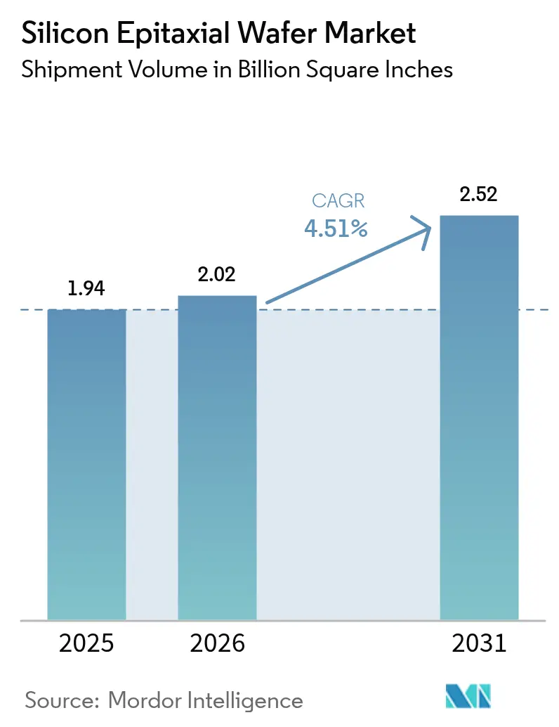
| Market Volume (2026) | 2.02 Billion Square Inches |
| Market Volume (2031) | 2.52 Billion Square Inches |
| Growth Rate (2026 - 2031) | 4.51% CAGR |
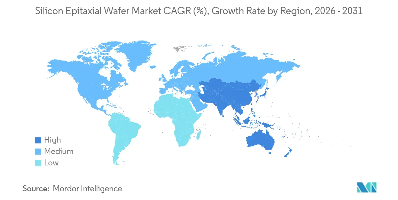
| Fastest Growing Market | Asia Pacific |
| Largest Market | Asia Pacific |
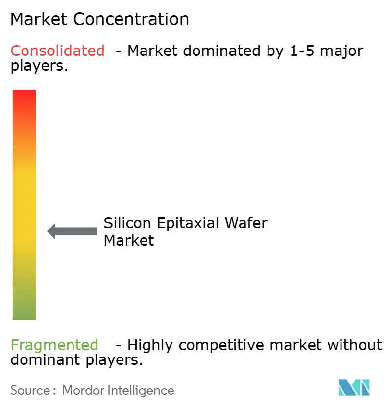
| Market Concentration | Medium |
Major Players *Disclaimer: Major Players sorted in no particular order Image © Mordor Intelligence. Reuse requires attribution under CC BY 4.0. | |
Silicon Epitaxial Wafer Market Analysis by Mordor Intelligence
The epitaxial silicon wafer market size is projected to expand from 1,938.59 million square inches in 2025, 2,018.27 million square inches in 2026, to 2,516.09 million square inches by 2031, registering a 4.51% CAGR over 2026-2031. Thicker, ultra-low-defect layers for 300 mm substrates, backside-power-delivery adoption, and rising demand from automotive electrification and on-device AI inference together underpin a durable volume floor. Asia-Pacific’s installed reactor base, government subsidies, and memory-capability additions keep regional output dominant, while quantum-computing prototypes on isotopically purified Si-28 layers point to a strategically important future niche. Capital expenditure above USD 120 million for an eight-reactor 300 mm line, coupled with volatile polysilicon feedstock pricing, pushes smaller suppliers to exit or consolidate. Incumbents are moving to renewable-powered cleanrooms and lower-temperature selective-epitaxy modules to satisfy carbon-footprint scrutiny and lithography overlay budgets below 1.5 nm.
Key Report Takeaways
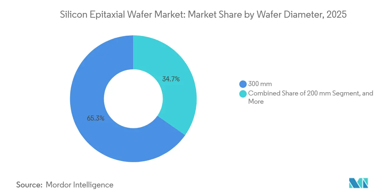
- By wafer diameter, the 300 mm format held 68.49% of 2025 volume, whereas the 200 mm category is on track for a 4.95% CAGR through 2031.
- By semiconductor device type, logic accounted for 35.73% of 2025 consumption, while discrete and power semiconductors are advancing at a 5.26% CAGR over 2026-2031.
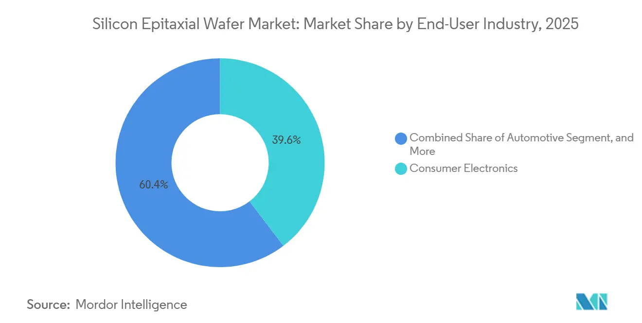
- By end-user, consumer electronics commanded 39.64% of 2025 shipments, yet automotive applications are the fastest mover with a 5.31% CAGR to 2031.
- By geography, Asia-Pacific secured 80.41% of the 2025 volume and is forecast to expand at a 5.58% CAGR through 2031.
Note: Market size and forecast figures in this report are generated using Mordor Intelligence’s proprietary estimation framework, updated with the latest available data and insights as of 2026.
Global Silicon Epitaxial Wafer Market Trends and Insights
Drivers Impact Analysis*
| Driver | (~) % Impact on CAGR Forecast | Geographic Relevance | Impact Timeline |
|---|---|---|---|
| Rising Demand for 300 mm Logic and Memory Capacity Expansions | +1.5% | Global, Concentrated in Taiwan, South Korea, United States | Medium Term (2–4 Years) |
| Semiconductor Device Scaling Driving Demand for Ultra-Low-Defect Density Epi Wafers | +1.2% | Global, Led by Taiwan and South Korea Foundries | Long Term (≥4 Years) |
| Surge in Automotive ADAS and Power Electronics Requiring High-Quality Epi Layers | +1.0% | Global, Early Gains in Europe, China, United States | Medium Term (2–4 Years) |
| Government Subsidies for Domestic 300 mm Wafer Fabs in Asia-Pacific | +0.9% | Asia-Pacific Core, Spill-Over to North America and Europe | Short Term (≤2 Years) |
| Adoption of Backside-Power-Delivery Architectures Boosting Epi Thickness Needs | +0.7% | Global, Pioneered by Leading-Edge Foundries in Taiwan and United States | Medium Term (2–4 Years) |
| Emergence of Quantum-Computing Qubits on Isotopically Purified Si-28 Epi Layers | +0.3% | North America and Europe Research Hubs | Long Term (≥4 Years) |
| Source: Mordor Intelligence | |||
Rising Demand for 300 mm Logic and Memory Capacity Expansions
Foundries and integrated device makers pledged USD 165 billion to new 300 mm fabs during 2025-2026, including TSMC’s Phoenix megafab, Samsung’s Taylor facility, and SK Hynix’s P&T7 plant.[1]TSMC Investor Relations, “Quarterly Results Q4 2025,” tsmc.com Together, these sites will require more than 50 million square inches of epitaxial wafers annually by 2028, and each 2 nm or 3 nm logic wafer needs a rigorously tuned layer to control threshold-voltage spread. Memory producers are stretching high-bandwidth-memory stacks to 12-16 layers, demanding thinner base wafers with engineered stress to avoid warpage in through-silicon-via drilling. The combined logic-memory pipeline stabilizes baseline demand and shields suppliers from the polished-wafer boom-bust pattern. Intel and TSMC’s backside-power-delivery roadmaps further compress tolerance to ±1% across a 300 mm-diameter.[2] Intel Corporation, “Technology Roadmap 2026,” intel.com
Semiconductor Device Scaling Driving Demand for Ultra-Low-Defect Density Epi Wafers
Gate-all-around transistors debuting at 3 nm and maturing at 2 nm cut the allowable defect density to below 0.01 cm-², a tenfold tightening compared to fin-FETs. Vertical nanosheet stacks amplify the damage caused by single dislocations, reducing drive current by up to 15%. Suppliers now pair in-situ hydrogen anneals with ultra-high-purity precursors, raising capital intensity but enabling node transitions. Reducing design rules for power and ground rails magnifies the penalty for epi-induced stress during extreme-ultraviolet exposure. The economic split pushes premium ultra-low-defect products to command 30-50% price premiums as stickier, longer contracts emerge.
Surge in Automotive ADAS and Power Electronics Requiring High-Quality Epi Layers
Automotive OEMs integrated an average 47 ADAS sensors per vehicle in 2025, each relying on mixed-signal ICs fabricated on 200 mm or 300 mm epitaxial wafers to meet ISO 26262 targets.[3]Continental AG, “Annual Report 2025,” continental.com Electric-vehicle inverters and chargers need 10-50 µm layers to sustain 650 V breakdown voltages with low conduction loss. STMicroelectronics and Infineon moved to secure in-house capacity in 2025, while tier-1 suppliers Bosch and Denso co-developed custom recipes under multi-year contracts. The emerging automotive supply chain prizes traceability and long qualification cycles, advantaging established producers and smoothing utilization rates.
Government Subsidies for Domestic 300 mm Wafer Fabs in Asia-Pacific
China mandates 50% domestic equipment content in new fabs by end-2026, accelerating local reactor development SCMP.COM. Japan allocated USD 6.8 billion to TSMC’s Kumamoto and Rapidus’s 2 nm pilot lines, stipulating local wafer sourcing. South Korea’s USD 19 billion package delivers tax credits and loans, prompting SK Siltron to invest 2.3 trillion won (USD 1.6 billion) through 2026 . India’s mission 2.0 offered USD 1.5 billion to its Gujarat project, with imports bridging near-term needs. Subsidies reduce capital cost for fabs, enabling larger and longer purchase commitments that justify new reactors at wafer suppliers.
Restraints Impact Analysis*
| Restraint | (~) % Impact on CAGR Forecast | Geographic Relevance | Impact Timeline |
|---|---|---|---|
| Escalating Capex for 300 mm Epitaxy Reactors and Automation | −0.8% | Global, Acute in Europe and North America | Short Term (≤2 Years) |
| Volatile Silicon Feedstock Prices Compressing Wafer Margins | −0.6% | Global, Severe in Commodity-Grade Segments | Medium Term (2–4 Years) |
| Carbon-Footprint Scrutiny of Energy-Intensive CVD Epitaxy Processes | −0.3% | Europe and North America, Spreading to Asia-Pacific | Medium Term (2–4 Years) |
| Lithography-Induced Pattern Collapse from Epi Stress Mismatches | −0.2% | Global, Concentrated at Leading-Edge Foundries | Long Term (≥4 Years) |
| Source: Mordor Intelligence | |||
Escalating Capex for 300 mm Epitaxy Reactors and Automation
A single 300 mm CVD reactor costs USD 12-15 million, and a greenfield line requires 8-12 reactors, plus USD 30-50 million in automation, bringing upfront investment to roughly USD 150-170 million before cleanroom fit-out. Smaller producers struggle to amortize that load, as Siltronic’s July 2025 exit from 150 mm production showed. In 2024-2025, rising interest rates led to an increase in the weighted-average cost of capital. This shift resulted in delays for certain expansions and favored established players who could leverage their balance-sheet cash.
Volatile Silicon Feedstock Prices Compressing Wafer Margins
Polysilicon transacted between USD 8 kg and USD 22 kg during 2024-2025.[4]Bloomberg, “Polysilicon Index 2025,” bloomberg.com Quarterly supply contracts create a lag that lets margin erosion linger months after spot declines. Wafer manufacturers grapple with a constraint: they can only pass on 3-5% of annual price hikes, compelling them to shoulder the brunt of rising costs. While some are eyeing vertical integration or forging renewable-powered offtake agreements, both avenues require substantial multi-year investments and come with unpredictable returns.
*Our forecasts treat driver/restraint impacts as directional, not additive. The impact forecasts reflect baseline growth, mix effects, and variable interactions.
Segment Analysis
By Wafer Diameter: Dual-Track Growth for 300 mm Dominance and 200 mm Revival
The 300 mm class delivered 68.49% of shipments in 2025, reflecting its centrality to leading-edge nodes and setting the baseline for the epitaxial silicon wafer market size. Backside power delivery lifts layer thickness by 15-20%, driving higher reactor utilization at Shin-Etsu and SUMCO. SEMI tightened flatness and bow limits by 30% since 2023, compelling suppliers to upgrade metrology and process control. Conversely, a retrofit wave in older fabs keeps 200 mm demand expanding at a 4.95% CAGR, defying earlier forecasts of terminal decline. Okmetic’s EUR 400 million (USD 452 million) Vantaa expansion, operational in 2026, doubled 200 mm capacity to serve automotive sensors and mixed-signal ICs, while Wafer Works and Episil also grew 200 mm output. The 150 mm and smaller pool is shrinking, yet niche optoelectronics players retain specialized capacity.
200 mm momentum is heavily automotive-driven, as power-module makers retrofit lines for silicon-carbide gate drivers and ADAS sensor ICs. China’s push for self-sufficiency in mature-node technology further elevates 200 mm volumes. Meanwhile, 300 mm investments stay concentrated in Asia-Pacific, cementing the region’s dominance in the epitaxial silicon wafer market.


By Semiconductor Device Type: Logic in Lead, Power Devices in Fast Lane
Logic consumed 35.73% of epitaxial volume in 2025 amid TSMC’s 3 nm and Samsung’s 2 nm ramps, using ultra-low-defect substrates to push initial yields above 70%. Discrete and power devices show the strongest trajectory with a 5.26% CAGR, as electric-vehicle inverters and industrial motor drives embrace thick epitaxial buffers. Memory’s share remains sizeable, with high-bandwidth-memory stacks requiring wafer thickness uniformity that supports 99% through-silicon-via yields, anchoring demand for premium substrates. Analog ICs keep a resilient niche for automotive sensor interfaces and power-management chips fabricated on cost-efficient 200 mm lines.
Photonic, sensor, and MEMS uses add further upside. Soitec’s silicon-on-insulator and photonics-SOI platforms scored hyperscale cloud design wins in 2025, proving that optical interconnect adoption can translate directly into epi wafer pull-through. Collectively, these trends diversify revenue streams and lessen reliance on the consumer-electronics cycle, supporting healthy dynamics for the epitaxial silicon wafer market share distribution.
By End-User: Consumer Electronics Bulk, Automotive Growth Catalyst
Consumer electronics accounted for 39.64% of 2025 shipments, with more than 2 billion smartphones, PCs, servers, and tablets embedded with epitaxial-based processors, modems, and PMICs. Automotive volumes are climbing fastest, riding a 5.31% CAGR as battery-electric-vehicle output hit 14 million units and semiconductor content per car multiplies. Industrial demand remains steady, especially for renewable-energy inverters, while 5G infrastructure and edge-computing nodes sustain telecoms demand even as initial deployment peaks slow.
Longer lead times, stricter traceability, and dual-source mandates in automotive contrast with the short cycles and inventory swings of consumer devices. The two end-markets therefore balance each other, smoothing utilization and pricing in the epitaxial silicon wafer market.
Geography Analysis
Asia-Pacific commanded 80.41% of 2025 volume and is projected to expand at a 5.58% CAGR through 2031. Taiwan leads advanced-logic output, South Korea dominates memory, and China’s self-reliance plan increases mature-node pulls, together underpinning the region’s share of the epitaxial silicon wafer market size. Japan’s USD 6.8 billion incentive package for TSMC Kumamoto and Rapidus ensures local supply continuity, while China’s export-control risks spur stockpiling by domestic fabs. India’s Gujarat project adds a future foothold, though initial wafers will be imported.
North America held a mid-single-digit slice in 2025 but benefits from the CHIPS and Science Act grants. GlobalWafers’ Sherman plant, opened in May 2025, and Intel’s Ohio megafab will together demand more than 10 million square inches a year by 2028. Europe lags on cost and permitting, yet Siltronic’s Singapore 300 mm line and GlobalWafers’ Novara, Italy site, opened in October 2025 with EUR 400 million (USD 452 million) in subsidies, secure automotive-focused supply routes. South America, along with the Middle East and Africa, remains import-dependent, with limited near-term prospects for indigenous capacity.
Regional concentration raises strategic-dependency alarms in the United States and Europe, prompting subsidy races and export controls. Still, Asia-Pacific’s reactor installed base, process know-how, and cluster economics make its dominance in the epitaxial silicon wafer market difficult to dislodge before the next decade.

Competitive Landscape
Shin-Etsu Handotai, SUMCO, GlobalWafers, Siltronic, and SK Siltron together command roughly 75% of 300 mm output, giving the epitaxial silicon wafer market a moderately high concentration profile. Their long-term supply agreements with TSMC, Samsung, Intel, and other leading fabs set reference pricing and reduce quarterly demand volatility. Each of these incumbents is investing in vertical integration, either through captive polysilicon assets or in-house epitaxy-reactor development, to defend gross margins as defect-density targets tighten.
Dual-source mandates from foundries raise the bar on thickness uniformity and inline metrology, pushing mid-tier suppliers such as Wafer Works and Episil Technologies to adopt machine-learning-based process control and advanced inspection tools. In parallel, China’s Simgui and Hebei Semiconductor are scaling capacity quickly under subsidy umbrellas, seizing share in mature-node logic and power devices and exerting downward pressure on commodity pricing. Specialty players focus on silicon-on-insulator, isotopically enriched Si-28, and 200 mm automotive-grade formats that command price premiums and longer qualification cycles.
Technology differentiation now hinges on reactor architecture, in-situ metrology, and stress-engineered epitaxial layers. ASM International and Tokyo Electron released next-generation tools in 2025 that lower defect counts by 40% and maintain ±0.5% thickness control across 300 mm diameters. Recent patent filings cluster around backside-power epitaxy, low-temperature growth for 3D integration, and isotopic purification techniques for quantum substrates, laying the groundwork for the next wave of competitive advantage.
Silicon Epitaxial Wafer Industry Leaders
Sumco Corporation
Shin-Etsu Handotai Co. Ltd.
GlobalWafers Co. Ltd.
Siltronic AG
SK Siltron Co. Ltd.
- *Disclaimer: Major Players sorted in no particular order

Recent Industry Developments
- February 2026: GlobalWafers began phase 2 design at Sherman, Texas, committing an additional USD 4 billion to double 300 mm capacity by 2028.
- January 2026: Okmetic reached volume production at its Vantaa, Finland expansion, doubling 150-200 mm capacity with ISO/TS 16949 certification.
- October 2025: GlobalWafers opened its Novara, Italy 300 mm plant, backed by EUR 400 million (USD 452 million) in EU subsidies.
- July 2025: Siltronic closed Burghausen, Germany 150 mm lines, reallocating focus to 300 mm automotive-grade output.


Global Silicon Epitaxial Wafer Market Report Scope
The Global Epitaxial Silicon Wafer Market Report is Segmented by Wafer Diameter (Up to 150 mm, 200 mm, 300 mm), Semiconductor Device Type (Logic, Memory, Analog, Discrete, Other), End-user (Consumer Electronics, Industrial, Telecommunications, Automotive, Other), and Geography (North America, Europe, Asia-Pacific, South America, Middle East and Africa). Market Forecasts are Provided in Terms of Volume (Million Square Inches).
| Up to 150 mm |
| 200 mm |
| 300 mm |
| Logic |
| Memory |
| Analog |
| Discrete |
| Other Semiconductor Device Types (Optoelectronics, Sensors, Micro) |
| Consumer Electronics | Mobile and Smartphones |
| PCs and Servers | |
| Industrial | |
| Telecommunications | |
| Automotive | |
| Other End-user Applications |
| North America | United States |
| Canada | |
| Mexico | |
| Europe | Germany |
| United Kingdom | |
| France | |
| Rest of Europe | |
| Asia-Pacific | China |
| Japan | |
| India | |
| South Korea | |
| Taiwan | |
| Rest of Asia-Pacific | |
| South America | |
| Middle East and Africa |
| By Wafer Diameter | Up to 150 mm | |
| 200 mm | ||
| 300 mm | ||
| By Semiconductor Device Type | Logic | |
| Memory | ||
| Analog | ||
| Discrete | ||
| Other Semiconductor Device Types (Optoelectronics, Sensors, Micro) | ||
| By End-user | Consumer Electronics | Mobile and Smartphones |
| PCs and Servers | ||
| Industrial | ||
| Telecommunications | ||
| Automotive | ||
| Other End-user Applications | ||
| By Geography | North America | United States |
| Canada | ||
| Mexico | ||
| Europe | Germany | |
| United Kingdom | ||
| France | ||
| Rest of Europe | ||
| Asia-Pacific | China | |
| Japan | ||
| India | ||
| South Korea | ||
| Taiwan | ||
| Rest of Asia-Pacific | ||
| South America | ||
| Middle East and Africa | ||


Key Questions Answered in the Report
How fast is demand for 300 mm epitaxial substrates growing?
Shipments for the 300 mm class rise at a 4.51% CAGR through 2031, anchored by logic and memory node transitions and thicker layers for backside power delivery.
Which end-market offers the highest growth momentum?
Automotive applications lead with a 5.31% CAGR to 2031 as electric-vehicle production scales and ADAS content increases.
Why is the 200 mm format still expanding despite 300 mm dominance?
Retrofits for power devices and mixed-signal ICs in legacy fabs drive 4.95% CAGR growth, especially for automotive and industrial demand.
How are suppliers mitigating feedstock price swings?
Strategies range from quarterly polysilicon hedging to vertical integration and renewable-powered long-term offtake agreements, though payoff spans several years.
What role do government subsidies play in regional wafer capacity?
Subsidy programs in China, Japan, South Korea, the United States, and India lower capital costs, encourage domestic sourcing, and secure multi-year supply contracts for new fabs.
Is the market exposed to environmental regulation risk?
Yes, carbon-footprint scrutiny of energy-intensive CVD epitaxy encourages adoption of renewable electricity and lower-temperature selective-epitaxy reactors to meet decarbonization goals.
Page last updated on:


