Asia-Pacific Semiconductor Silicon Wafer Market Size and Share
Market Overview
| Study Period | 2020 - 2031 |
|---|---|
| Forecast Data Period | 2026 - 2031 |
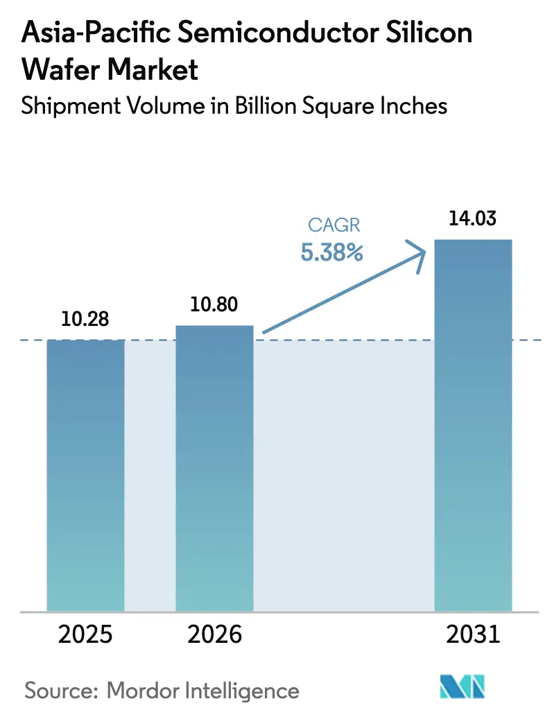
| Base Year Market Size (2025) | 10.28 Billion Square Inches |
| Market Volume (2026) | 10.80 Billion Square Inches |
| Market Volume (2031) | 14.03 Billion Square Inches |
| Growth Rate (2026 - 2031) | 5.38% CAGR |
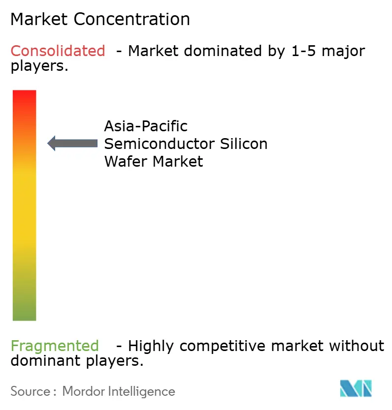
| Market Concentration | High |
Major Players *Disclaimer: Major Players sorted in no particular order Image © Mordor Intelligence. Reuse requires attribution under CC BY 4.0. | |
Asia-Pacific Semiconductor Silicon Wafer Market Analysis by Mordor Intelligence
The Asia-Pacific Semiconductor Silicon Wafer Market size in terms of shipment volume was valued at 10.28 Billion Square Inches in 2025 and is estimated to grow from 10.80 Billion Square Inches in 2026 to reach 14.03 Billion Square Inches by 2031, at a CAGR of 5.38% during the forecast period (2026-2031). Rising sovereign-chip programs across China, India, Japan, and South Korea are driving new fab construction, while hyperscale data centers and 5G devices keep demand for 300 mm prime-polished substrates elevated. Planned mega-clusters in Yongin, Pyeongtaek, Tainan, Gujarat, and Hokkaido have already secured multi-year wafer supply, shortening procurement cycles and tightening the merchant pool. Simultaneously, the shift toward silicon-on-insulator for radio-frequency front-end modules and the migration of power devices to silicon-carbide and gallium-nitride are reshaping the mix, freeing mature 200 mm capacity for analog and discretes. Price pressure from energy inflation remains a headwind, yet vertical integration and renewable-energy contracts are cushioning leading producers.
Key Report Takeaways
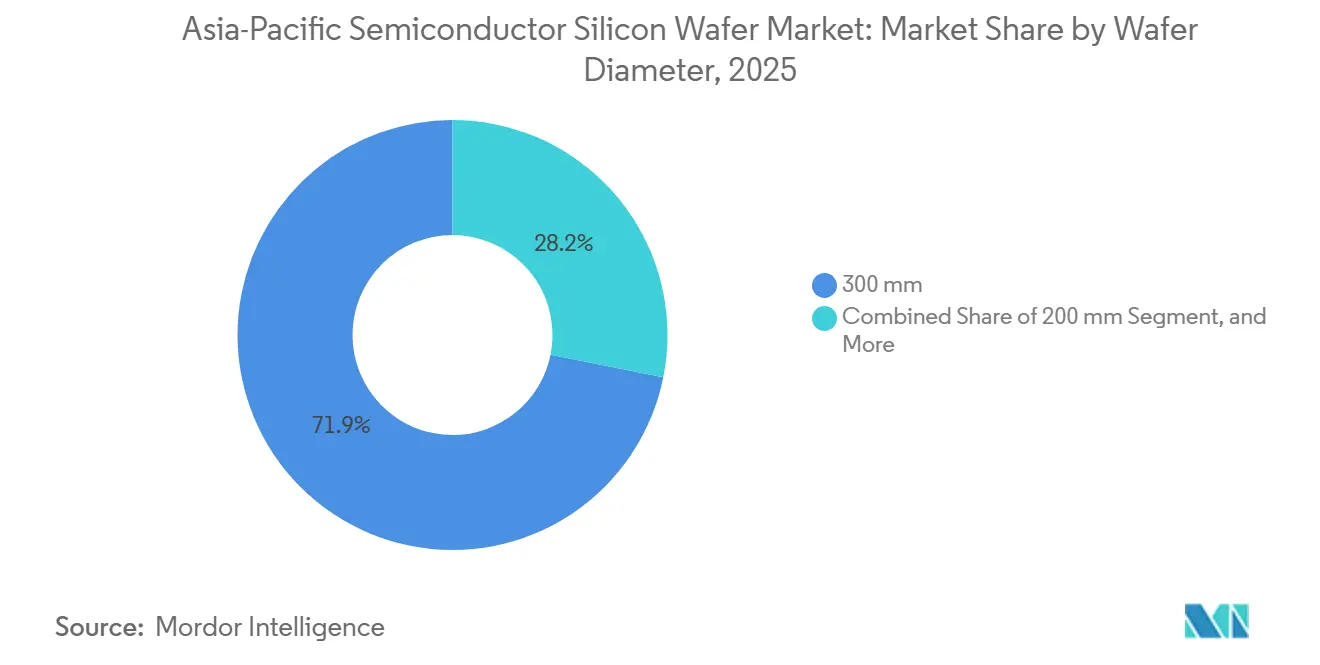
- By wafer diameter, 300 mm products captured 71.85% of 2025 volume, while the 300 mm segment is projected to expand at a 5.99% CAGR through 2031.
- By semiconductor device type, logic held 33.59% of the Asia-Pacific semiconductor silicon wafer market share in 2025 and is poised to grow at 5.75% through 2031.
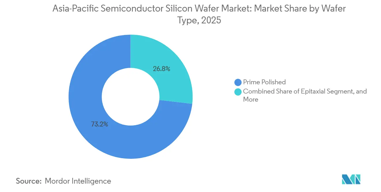
- By wafer type, prime-polished substrates accounted for 73.19% of 2025 demand; silicon-on-insulator is the fastest-growing category, with a 6.07% CAGR to 2031.
- By end-user, consumer electronics led with a 40.62% of the Asia-Pacific semiconductor silicon wafer market share in 2025, while automotive applications are projected to record the highest CAGR at 6.21% through 2031.
- By geography, China accounted for 63.37% of regional wafer output in 2025; India is the fastest-growing geography, advancing at a 6.11% CAGR through 2031.
Note: Market size and forecast figures in this report are generated using Mordor Intelligence’s proprietary estimation framework, updated with the latest available data and insights as of January 2026.
Figures recorded within Asia feed into a worldwide estimate while studying the global industry. Mordor Intelligence's semiconductor silicon wafer market size captures this aggregation.
Asia-Pacific Semiconductor Silicon Wafer Market Trends and Insights
Drivers Impact Analysis*
| Driver | (~) % Impact on CAGR Forecast | Geographic Relevance | Impact Timeline |
|---|---|---|---|
| Soaring 5G smartphone penetration boosting 300 mm wafer demand | +1.2% | China, India, South Korea, Southeast Asia | Medium term (2-4 years) |
| Government subsidies for domestic semiconductor manufacturing | +1.5% | China, India, Japan, South Korea, Taiwan | Long term (≥4 years) |
| Rapid deployment of AI data centers requiring advanced logic nodes | +1.3% | China, Japan, South Korea, Singapore | Short term (≤2 years) |
| Silicon-carbide and GaN transition freeing 200 mm capacity | +0.6% | Japan, China, South Korea | Medium term (2-4 years) |
| Surging demand for photonic integrated circuits in telecom gear | +0.4% | China, Japan, South Korea, Taiwan | Medium term (2-4 years) |
| Adoption of backside power-delivery networks increasing CMP steps | +0.3% | Taiwan, South Korea, China | Short term (≤2 years) |
| Source: Mordor Intelligence | |||
Soaring 5G Smartphone Penetration Boosting 300 mm Wafer Demand
A steep rise in 5G handset shipments is shifting front-end modules and application processors onto 300 mm substrates that support sub-5 nm lithography. Mainland assemblers shipped more than 280 million 5G smartphones in 2025, and India ended the same year with 180 million 5G subscribers. Foundries in Tainan, Hwaseong, and Shanghai are therefore operating at near full utilization for 4 nm and 3 nm nodes. Radio-frequency silicon-on-insulator uptake has accelerated as millimeter-wave designs mandate ultra-low loss substrates. Longer upgrade cycles for premium phones paradoxically lift total silicon content per unit, stabilizing wafer pull even when unit sales plateau.[1]Taiwan Semiconductor Manufacturing Company, “Corporate Sustainability Report 2025,” tsmc.com
Government Subsidies for Domestic Semiconductor Manufacturing
Fiscal incentives now dominate capital-expenditure roadmaps across the region. The Japanese cabinet earmarked JPY 2 trillion (USD 13.5 billion) for a 2 nm foundry in Hokkaido, and India’s Semiconductor Mission raised its incentive pool to USD 15 billion. South Korea raised tax credits to 25% of cap-ex, encouraging an additional KRW 120 trillion (USD 91 billion) commitment in Yongin. China’s third National IC Fund injected CNY 344 billion (USD 47 billion) into mature-node expansions. These subsidies lock in large wafer call-offs under long-term contracts, thereby shrinking spot-market availability and nudging prices upward despite new capacity.[2]Shin-Etsu Chemical Co. Ltd., “Medium-Term Management Plan 2026,” shinetsu.co.jp
Rapid Deployment of AI Data Centers Requiring Advanced Logic Nodes
Hyperscalers purchased more than 2.8 million AI accelerators in 2025. Each next-generation tensor device consumes a larger die area and thicker high-bandwidth-memory stacks, which lower per-wafer yield. To meet schedules, Taiwan Semiconductor Manufacturing Company and Samsung Foundry together cleared an additional 1.1 million wafer equivalents for AI logic and memory. This single driver is forecast to add roughly 1.3 percentage points to the regional CAGR through 2028 as capital spending on AI clusters remains front-loaded.[3]Samsung Electronics Co. Ltd., “Foundry Roadmap Update 2025,” samsung.com
Silicon-Carbide and GaN Transition Freeing 200 mm Capacity
Automotive traction inverters and telecom power amplifiers are migrating to silicon carbide and gallium nitride substrates. The movement frees mature 200 mm silicon lines for analog, sensor, and microcontroller output, easing the post-pandemic crunch on legacy nodes. As spot prices for 200 mm prime-polished wafers retreated toward USD 90 per piece in early 2026, utilization rates at specialty suppliers remained above 90%, providing high-resistivity material for radio-frequency switches at a 25%-plus margin.
Restraints Impact Analysis*
| Restraint | (~) % Impact on CAGR Forecast | Geographic Relevance | Impact Timeline |
|---|---|---|---|
| Chronic shortages of ultrapure polysilicon feedstock | -0.9% | China, Japan, South Korea, Taiwan | Short term (≤2 years) |
| Escalating energy prices in East Asia impacting wafer-fab costs | -0.7% | South Korea, Japan, Taiwan | Medium term (2-4 years) |
| US export controls on advanced tools delaying capacity expansions | -0.5% | China | Long term (≥4 years) |
| High defect density in 450 mm pilot lines hindering investments | -0.2% | Global (pilot work in Japan and Taiwan) | Long term (≥4 years) |
| Source: Mordor Intelligence | |||
Chronic Shortages of Ultrapure Polysilicon Feedstock
Polysilicon production in Xinjiang fell 18% in late 2025 following energy-rationing directives, pushing spot prices above USD 30 per kg and inflating raw-material costs by double digits for wafer producers without captive feedstock. While Tokuyama and OCI are adding 25,000 metric tons of new fluidized-bed capacity, commercial output will not arrive before 2027. Larger players such as Shin-Etsu Chemical and SUMCO protect margins through upstream integration, leaving smaller rivals saddled with 8-to-12-week lead-time extensions.
Escalating Energy Prices in East Asia Impacting Wafer-Fab Costs
Utility tariffs in South Korea, Japan, and Taiwan climbed by 9% to 14% during 2025-2026 amid soaring liquefied natural gas import bills. Energy now accounts for roughly 40% of total wafer-processing costs. SK Siltron’s Gumi fab, which consumes 1.2 million 300 mm wafers monthly, saw annual electricity expenses rise by USD 34 million after the April 2025 rate hike. Responding, Siltronic installed waste-heat recovery in Singapore, trimming energy intensity 11% and setting a new cost-containment benchmark.
*Our forecasts treat driver/restraint impacts as directional, not additive. The impact forecasts reflect baseline growth, mix effects, and variable interactions.
Segment Analysis
By Wafer Diameter: Rising 300 mm Dominance
The 300 mm class accounted for 71.85% of total shipments in 2025, driven by logic and high-bandwidth memory scaling. Asia-Pacific semiconductor silicon wafer market size for 300 mm substrates is expected to expand faster than the overall baseline as gate-all-around transistors at 2 nm inflate die area and drive per-chip wafer pull. Installed base already spans 42 fabs across the region, and Shin-Etsu’s Shirakawa plant alone lifted epitaxial output to 800,000 wafers per month in 2025.
Mature 200 mm lines continue to serve analog power and sensor applications, buffered by capacity freed up by silicon-carbide migration. Wafers up to 150 mm remain a sub-5% niche for gallium arsenide and indium phosphide devices. Cost-of-ownership challenges leave 450 mm pilots in a quandary, as defect densities remain thrice the threshold for break-even yields. This persistent issue highlights the significant technical and economic barriers that need to be addressed before 450 mm technology can achieve commercial viability. Consequently, this setback postpones any shake-up to the established 300 mm supply chain, which continues to dominate the semiconductor manufacturing landscape.


By Semiconductor Device Type: Logic Ascendancy
Logic devices accounted for 33.59% of shipments in 2025, lifted by AI, 5G basebands, and custom accelerators. Asia-Pacific semiconductor silicon wafer market share for logic is supported by record reticle counts that raise wafer consumption per chip, while heterogeneous integration adds to substrate demand. Memory followed at roughly 30%, with high-bandwidth-memory stacks driving thicker grind steps and thinner finished wafers.
Analog and discrete together absorb most of the newly liberated 200 mm supply, serving automotive powertrains and industrial automation. As lidar and time-of-flight technologies gain traction, the combined wafer pull for sensors, MEMS, and optoelectronics—each holding a high single-digit share—continues to rise. These components play a critical role in various applications, including automotive, consumer electronics, and industrial sectors, driving their steady growth. This diversification strategy helps suppliers weather the cyclical fluctuations of smartphone sales, ensuring a more stable revenue stream.
By Wafer Type: Prime Polished Tops, SOI Gains Momentum
In 2025, prime polished materials accounted for 73.19% of the regional volume, aligning with mainstream logic and memory needs that demand defect densities below 0.08 cm-². The Asia-Pacific market for semiconductor silicon wafers, particularly prime-polished substrates, is set to align with rising demand. This is driven by the need for ultra-thin base wafers in backside power-delivery networks, which can endure extra CMP cycles. The increasing adoption of advanced semiconductor technologies and the growing demand for high-performance computing applications further contribute to the expansion of this segment.
Silicon-on-insulator, growing at a brisk 6.07% CAGR, is gaining traction, especially in radio-frequency front-end and low-power MCU designs. Epitaxial wafers, holding a 15% market share, are bolstered by demand from power semiconductors and CMOS image sensors. Specialty silicon, encompassing high-resistivity and sensor-grade variants, consistently captures a 6% market share. However, it commands premium pricing, a reflection of its stringent thickness and dopant specifications. The rising focus on energy-efficient devices and the integration of advanced sensor technologies are expected to drive further growth in these specialty silicon segments.
By End-User: Consumer Electronics Leads, Automotive Accelerates
In 2025, consumer electronics, spearheaded by smartphones, tablets, and wearables, dominated wafer usage with a 40.62% share. The Asia-Pacific market for semiconductor silicon wafers, closely tied to mobile devices, showcases resilience. This is largely due to the rising content of 5G units, which compensates for otherwise plateauing volumes. The increasing adoption of advanced technologies in consumer electronics, such as foldable displays and augmented reality (AR) features, further drives demand for semiconductor wafers. Meanwhile, PCs and servers, bolstered by AI workstations and edge nodes, command a stable mid-teens market share.
Automotive stands out as the primary growth driver, boasting a 6.21% CAGR projected through 2031. Notably, battery-electric platforms now incorporate up to 3,500 semiconductor devices per vehicle, a figure that surpasses internal-combustion models by more than fourfold. The growing trend of autonomous driving and connected vehicles is also significantly contributing to the demand for semiconductor wafers in the automotive sector. Additionally, the industrial and telecom infrastructure sectors, fueled by Industry 4.0 retrofits and 5G base-station rollouts, contribute significantly, together representing about one-fifth of total shipments. The integration of IoT devices and smart manufacturing solutions further enhances the demand for wafers in these segments.
Geography Analysis
China captured 63.37% of Asia-Pacific shipments in 2025, reflecting both domestic electronics demand and an aggressive build-out of mature-node capacity. National IC Fund Phase III deployed CNY 344 billion (USD 47 billion) to broaden 14 nm-28 nm output, while export-control limitations continue to curtail sub-7 nm aspirations. Japan followed at about a 12% share, anchored by Shin-Etsu Chemical and SUMCO, which supply more than half of the world’s 300 mm blanks.
Samsung Electronics and SK Hynix, two giants from South Korea, jointly consumed 1.9 million 300 mm wafers monthly for DRAM, NAND, and high-bandwidth memory, giving the nation a 14% market share. South Korea's stronghold in the semiconductor market is further reinforced by its advanced manufacturing capabilities and significant investments in R&D. Taiwan, holding an 8% share, wields greater strategic influence: Taiwan Semiconductor Manufacturing Company dominates the global processing of sub-7 nm logic and procures 85% of its blanks locally. Taiwan's role as a critical player in the semiconductor supply chain is underscored by its technological leadership and robust local sourcing strategies.
India, buoyed by a USD 15 billion incentive scheme, is on a rapid ascent, projected to grow at a 6.11% CAGR through 2031. With three greenfield fabs greenlit in 2025, the demand is set to surge, requiring an extra 120,000 wafers monthly by 2030. This growth trajectory highlights India's ambition to establish itself as a key player in the global semiconductor landscape, supported by favorable government policies and increasing foreign investments. Meanwhile, the rest of Asia, encompassing Singapore, Malaysia, and Australia, made up the final 3%, reaping rewards from supply-chain diversification efforts by U.S. and European clients. These regions have benefited from their strategic positioning and efforts to attract semiconductor investments, further strengthening their role in the global supply chain.
Mordor Intelligence evaluates the semiconductor silicon wafer market across all key regional markets, including Europe and North America, with deeper country-level insights covering South Korea, Taiwan, Japan, India, China, Germany, and United States.
Competitive Landscape
Market concentration is moderate: the top three suppliers, Shin-Etsu Chemical, SUMCO Corporation, and GlobalWaferscontrolled close to 68% of 300 mm shipments and 55% of 200 mm volume in 2025. Integrated device manufacturers now lock in 40-50% of merchant capacity through decade-long supply agreements, squeezing independents. Shin-Etsu’s JPY 180 billion (USD 1.2 billion) Shirakawa expansion and SUMCO’s 10-year pact with Samsung illustrate the trend toward tighter vertical alignment.
Specialty producers are establishing strong footholds in high-resistivity, sensor-grade, and ultra-thin substrates, driven by increasing demand across various applications. Soitec is at the forefront of radio-frequency SOI, leveraging its expertise to cater to the growing needs of advanced communication technologies. Meanwhile, Wafer Works has achieved ISO 26262 functional-safety certification for its sensor wafers, which are pivotal for automotive lidar, ensuring enhanced safety and reliability in autonomous vehicles. Ferrotec, leveraging its proprietary magnetic-fluid technology, has not only enhanced crystal-pulling yields but is also scaling its revamped 200 mm lines in Singapore to meet the rising global demand for high-quality substrates.
Chinese challengers Zhonghuan Semiconductor and Shanghai Simgui doubled their 300 mm output but still trail Japanese peers by one to two technology nodes in epitaxial uniformity and defect control. Patent filings for atomic-layer deposition on wafer backsides rose 42% year on year, led by Taiwan Semiconductor Manufacturing Company, Samsung, and Applied Materials, signaling a rapid shift toward backside power-delivery designs that demand ultra-flat substrates.
Asia-Pacific Semiconductor Silicon Wafer Industry Leaders
Shin-Etsu Chemical Co., Ltd.
SUMCO Corporation
GlobalWafers Co., Ltd.
SK Siltron Co., Ltd.
Siltronic AG
- *Disclaimer: Major Players sorted in no particular order

Recent Industry Developments
- February 2026: Shin-Etsu Chemical announced a JPY 180 billion (USD 1.2 billion) expansion of its Shirakawa plant, adding 200,000 300 mm epitaxial wafers per month by mid-2028.
- January 2026: SUMCO Corporation finalized a 10-year agreement to supply 1.5 million 300 mm prime polished wafers annually to Samsung Electronics.
- December 2025: GlobalWafers completed phase 2 of its Texas fab, investing an additional USD 4 billion to lift 300 mm capacity by 1.2 million wafers per month by 2027.
- November 2025: SK Siltron committed KRW 3.5 trillion (USD 2.6 billion) for a new 300 mm facility in Gumi, with start-up slated for early 2028.


Asia-Pacific Semiconductor Silicon Wafer Market Report Scope
The Asia-Pacific Semiconductor Silicon Wafer Market Report is Segmented by Wafer Diameter (Up to 150 mm, 200 mm, 300 mm), Semiconductor Device Type (Logic, Memory, Analog, Discrete, Other Semiconductor Device Types), Wafer Type (Prime Polished, Epitaxial, Silicon-on-Insulator (SOI), Specialty Silicon), End-user (Consumer Electronics, Mobile and Smartphones, PCs and Servers, Industrial, Telecommunications, Automotive, Other End-user Applications), and Geography (China, Japan, South Korea, Taiwan, India, Rest of Asia-Pacific). The Market Forecasts are Provided in Terms of Shipment Volume (Square Inches).
| Up to 150 mm |
| 200 mm |
| 300 mm |
| Logic |
| Memory |
| Analog |
| Discrete |
| Other Semiconductor Device Types, Optoelectronics, Sensors, Micro |
| Prime Polished |
| Epitaxial |
| Silicon-on-Insulator, SOI |
| Specialty Silicon, High-Resistivity, Power, Sensor-Grade |
| Consumer Electronics |
| Mobile and Smartphones |
| PCs and Servers |
| Industrial |
| Telecommunications |
| Automotive |
| Other End-user Applications |
| China |
| Japan |
| South Korea |
| Taiwan |
| India |
| Rest of Asia-Pacific |
| By Wafer Diameter | Up to 150 mm |
| 200 mm | |
| 300 mm | |
| By Semiconductor Device Type | Logic |
| Memory | |
| Analog | |
| Discrete | |
| Other Semiconductor Device Types, Optoelectronics, Sensors, Micro | |
| By Wafer Type | Prime Polished |
| Epitaxial | |
| Silicon-on-Insulator, SOI | |
| Specialty Silicon, High-Resistivity, Power, Sensor-Grade | |
| By End-user | Consumer Electronics |
| Mobile and Smartphones | |
| PCs and Servers | |
| Industrial | |
| Telecommunications | |
| Automotive | |
| Other End-user Applications | |
| By Geography | China |
| Japan | |
| South Korea | |
| Taiwan | |
| India | |
| Rest of Asia-Pacific |


Key Questions Answered in the Report
How large will Asia-Pacific silicon wafer demand be by 2031?
Shipments are projected to reach 14.04 billion square inches by 2031, reflecting a 5.38% compound annual growth rate from 2026.
Which wafer diameter is expanding fastest?
The 300 mm class grows quickest at 5.99% CAGR through 2031, buoyed by advanced logic and high-bandwidth-memory requirements.
Why is automotive consumption rising so sharply?
Battery-electric vehicles pack up to 3,500 chips per car, more than quadruple internal-combustion designs, lifting automotive wafer demand at a 6.21% CAGR.
Which countries benefit most from subsidy programs?
China, India, Japan and South Korea collectively deploy more than USD 165 billion in incentives, accelerating localized wafer and fab capacity.
What risks constrain near-term supply?
Ultrapure polysilicon shortages and rising East-Asian energy tariffs squeeze margins and prolong lead times for smaller wafer producers.
Who ranks as the leading wafer suppliers?
Shin-Etsu Chemical, SUMCO Corporation and GlobalWafers jointly control about two-thirds of 300 mm shipments, with specialty niches held by Soitec, Wafer Works and Ferrotec.
Page last updated on:


