Taiwan LED Epitaxy MOCVD Equipment Market Size and Share
Market Overview
| Study Period | 2020 - 2031 |
|---|---|
| Forecast Data Period | 2026 - 2031 |
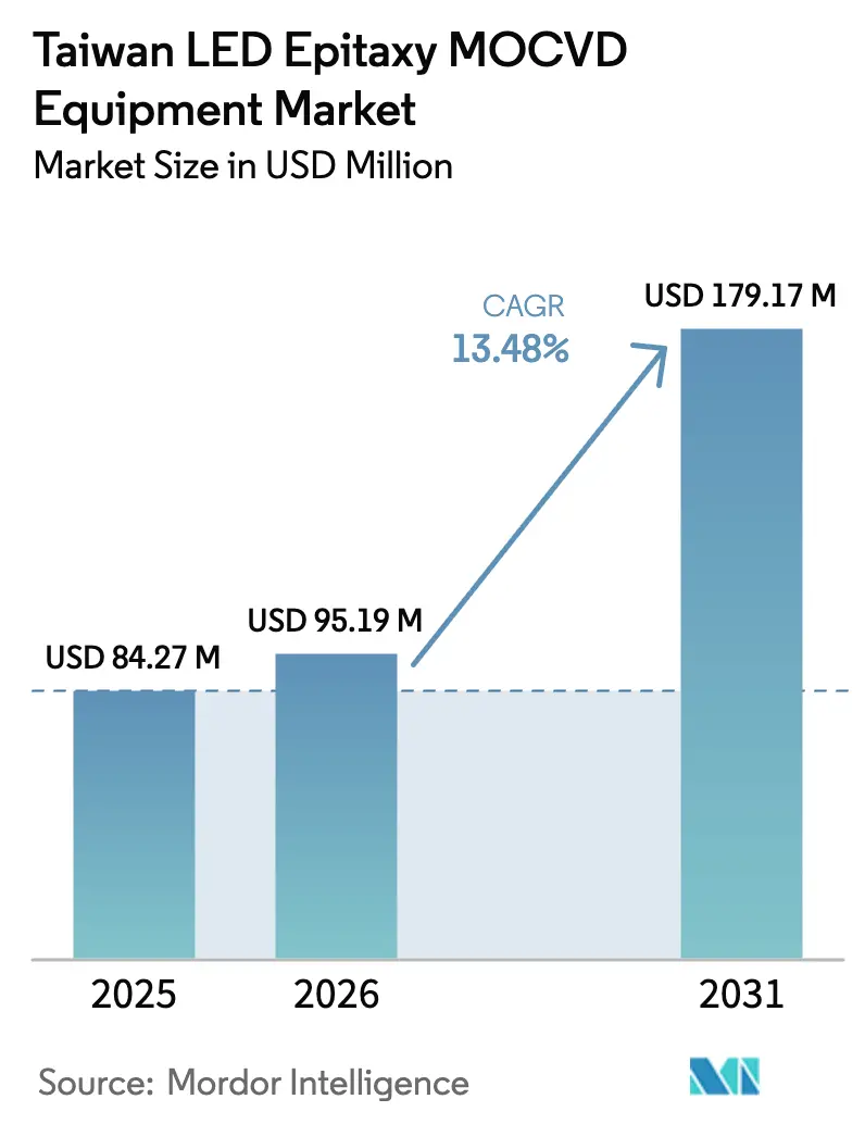
| Base Year Market Size (2025) | USD 84.27 Million |
| Market Size (2026) | USD 95.19 Million |
| Market Size (2031) | USD 179.17 Million |
| Growth Rate (2026 - 2031) | 13.48% CAGR |
| Market Concentration | Medium |
Major Players *Disclaimer: Major Players sorted in no particular order Image © Mordor Intelligence. Reuse requires attribution under CC BY 4.0. | |
Taiwan LED Epitaxy MOCVD Equipment Market Analysis by Mordor Intelligence
The Taiwan LED epitaxy MOCVD equipment market size was valued at USD 84.27 million in 2025 and is estimated to grow from USD 95.19 million in 2026 to reach USD 179.17 million by 2031, at a CAGR of 13.48% during the forecast period (2026-2031). Demand accelerates as Taiwanese fabs scale compound-semiconductor capacity, shift to 200 mm and 300 mm GaN-on-Si wafers, and capture surging orders from micro-LED, ultraviolet sterilization, and GaN power-device producers. Large integrated device manufacturers intensified capital spending in 2025-2026 after export-control changes heightened the need for localized, geopolitically resilient supply chains, while government subsidies covering AI-driven yield-improvement projects shorten payback periods for new reactor clusters. Equipment makers that combine high throughput, narrow uniformity windows, and wafer-size flexibility dominate ordering patterns, although multi-reactor cluster prices above USD 10 million continue to curb smaller foundry expansions. Competitive dynamics focus on 300 mm GaN systems, AI-enabled process control, and greener gas-handling modules that help buyers meet emerging sustainability disclosure rules.
Key Report Takeaways
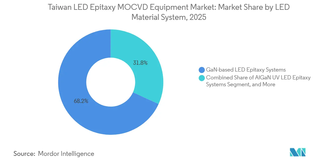
- By LED material system, GaN-based LED epitaxy systems led with 68.19% market share in 2025, while the AlGaN ultraviolet LED epitaxy systems segment is expanding at a 14.53% CAGR through 2031.
- By wafer-size capability, the 150 mm segment accounted for 48.14% of the Taiwan LED epitaxy MOCVD equipment market share in 2025; systems supporting the 200 mm and above segment is rising at 14.38% CAGR to 2031.
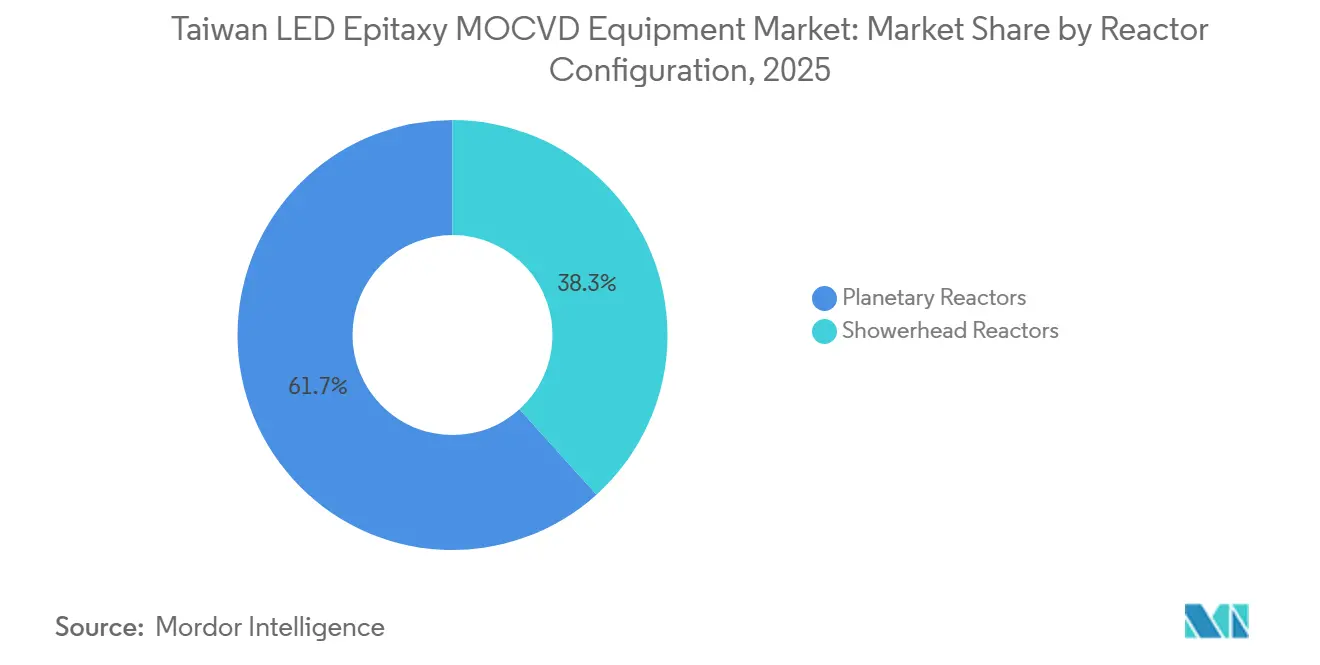
- By reactor configuration, planetary reactors held 61.68% share of the Taiwan LED epitaxy MOCVD equipment market size in 2025, whereas the showerhead reactors segment is progressing at a 14.62% CAGR to 2031.
- By end user, integrated LED manufacturers commanded 71.76% of market share in 2025, but the epitaxy foundries and merchant Epi suppliers segment is forecast to post a 14.46% CAGR over 2026-2031.
Note: Market size and forecast figures in this report are generated using Mordor Intelligence’s proprietary estimation framework, updated with the latest available data and insights as of January 2026.
Worldwide, activity is shaped by contributions from multiple countries and regions, with Taiwan representing one among them. The global report on led epitaxy mocvd equipment market by Mordor Intelligence reflects how these countries and regional layers combine into a single system.
Taiwan LED Epitaxy MOCVD Equipment Market Trends and Insights
Drivers Impact Analysis*
| Driver | (~) % Impact on CAGR Forecast | Geographic Relevance | Impact Timeline |
|---|---|---|---|
| Growing Mini-LED Backlighting Adoption in Consumer Electronics | +2.8% | Global, centered on Taiwan’s supply chain for notebook, tablet, TV, and gaming-monitor brands | Medium term (2-4 years) |
| Taiwan’s Government Subsidies for Compound Semiconductor Expansion | +1.9% | National focus on Hsinchu, Jhunan, and Chunan science parks | Short term (≤ 2 years) |
| Local Supply-Chain Localization to Mitigate Cross-Strait Risks | +2.1% | Taiwan core with spillover to Japan and the United States | Long term (≥ 4 years) |
| Rapid Capacity Upgrades Toward 200 mm GaN Wafers | +2.3% | Asia-Pacific core, notably Taiwan and Japan | Medium term (2-4 years) |
| Increasing Demand for Deep-UV Sterilization LEDs Post-COVID-19 | +1.6% | Global healthcare, water, and air-purification segments | Medium term (2-4 years) |
| Energy-Efficiency Mandates Driving Phosphor-Free Micro-LED Development | +1.4% | Global, guided by European Union and U.S. standards | Long term (≥ 4 years) |
| Source: Mordor Intelligence | |||
Growing Mini-LED Backlighting Adoption in Consumer Electronics
Consumer-electronics brands accelerated mini-LED use in premium laptops, tablets, televisions, and high-refresh-rate gaming monitors. Taiwanese chipmakers shifted capacity from traditional LEDs to mini-LED formats, raising wafer shipments and pushing reactor utilization close to round-the-clock schedules. The tight demand profile shortened lead times for new tools, compelling fabs to pull forward 200 mm platform purchases so they could boost square-centimeter output per run. Micro-LED momentum in wearables and augmented-reality headsets overlaps these investments, yet imposes stricter wavelength-uniformity targets that favor single-wafer or showerhead architectures. The resulting dual-track demand pattern, high-throughput planetary reactors for cost-sensitive backlighting dies alongside precision tools for micro-display pixels, allows suppliers with both product classes to widen their installed-base footprints.[1]Bettywu, “Shortage Caused by Explosive Growth in Mini LED Demand,” LEDinside, ledinside.com
Taiwan’s Government Subsidies for Compound Semiconductor Expansion
The Ministry of Economic Affairs introduced an AI Industry Innovation Programme that reimburses up to 50% of qualified equipment outlays when projects embed AI-driven process control, predictive maintenance, or yield-optimization modules. Eligibility criteria favor Taiwanese ownership and local IP commercialization, nudging foreign suppliers to establish deeper engineering, service, and part-fabrication operations on the island. Subsidized tools can be synchronized with 1- to 3-year micro-LED or GaN power-device ramps, reducing cash-flow strain and smoothing qualification timetables.[2]Pertama Partners, “Taiwan MOEA AI Industry Innovation Programme 2026,” pertamapartners.com As subsidies overlap with broader silicon-photonics initiatives, fabs integrate MOCVD reactors with co-packaged optics lines, reinforcing buyer preference for energy-efficient reactors that already meet forthcoming Scope 3-emissions reporting rules.
Local Supply-Chain Localization to Mitigate Cross-Strait Risks
Taiwan expanded its entity list in 2025, aligning export-licensing rules with U.S. controls and raising compliance costs on equipment or components headed to mainland Chinese customers. Fabs now require vendors to hold domestic spare-parts depots, localize repair turnarounds, and provide on-island process-integration engineers. Friendshoring moves by U.S. and European partners encourage joint research projects in Taiwan, rewarding suppliers that publish transparent life-cycle assessments and energy-consumption metrics for their tools. This environment favors incumbents with embedded Taiwan service teams and could marginalize low-cost imports lacking a robust local footprint.
Rapid Capacity Upgrades Toward 200 mm GaN Wafers
Alliances between Ennostar and ALLOS plus Powerchip’s assumption of TSMC’s GaN volumes triggered a decisive pivot toward 200 mm lines designed for micro-LED and power-device scale-up. The leap demands reactors with tighter thermal gradients, lower defect densities, and recipe libraries that port smoothly from 150 mm to 200 mm carriers. Equipment bids now routinely bundle inline metrology and AI-assisted run-to-run controls that qualify for government co-funding, making advanced platforms more affordable for mid-tier fabs. Suppliers with proven 300 mm capability secure long-lead orders as customers future-proof expansion roadmaps.
Restraints Impact Analysis*
| Restraint | (~) % Impact on CAGR Forecast | Geographic Relevance | Impact Timeline |
|---|---|---|---|
| High Capital Cost of Multi-Reactor MOCVD Clusters | -1.7% | Global, more severe for smaller Taiwan foundries | Short term (≤ 2 years) |
| Technical Complexity in AlGaN UV LED Uniformity Control | -1.3% | Taiwan, Japan, and Korea UV LED factories | Medium term (2-4 years) |
| Talent Shortage in Epitaxy Process Engineering | -0.9% | Taiwan and neighboring recruiting markets | Long term (≥ 4 years) |
| Import Dependency on Critical MOCVD Components | -0.8% | Taiwan and other Asia-Pacific buyers reliant on U.S. and EU parts | Medium term (2-4 years) |
| Source: Mordor Intelligence | |||
High Capital Cost of Multi-Reactor MOCVD Clusters
Cutting-edge reactor suites configured for eight 6-inch or six 8-inch wafers cost upward of USD 10 million, including wafer-handling robots, in-situ metrology, abatement, and gas cabinets. Smaller merchant epitaxy houses run on thinner gross-margin structures than integrated peers, making self-financed cluster purchases prohibitive. Even with 50% subsidy coverage, applicants must fund the remaining amount in cash or loans and absorb extended depreciation cycles. Aftermarket service contracts and consumable kits add around a quarter to lifetime ownership costs, embedding a recurring expense line that deters speculative capacity additions. Consequently, foundries often stretch existing fleets, accept lower throughput per chamber, and delay entering new wavelength niches until anchor customers commit to multiyear wafer-take agreements.[3]AIXTRON SE, “Planetary Principle (MOCVD),” aixtron.com
Technical Complexity in AlGaN UV LED Uniformity Control
Deep-UV LEDs require aluminum-rich quantum wells and electron-blocking layers whose composition must stay within a narrow window across each 4- or 6-inch wafer. Growth temperatures above 1,100 °C, very high V/III precursor ratios, and ultrathin monolayer structures increase risk of non-uniform Al incorporation, leading to wavelength shift and yield loss. Achieving high p-type doping in aluminum-rich layers remains difficult, because magnesium activation energies rise sharply with Al content. Only a handful of Taiwanese fabs can consistently hit the necessary threading dislocation densities, and each new reactor recipe can take months to stabilize. These hurdles slow capex decisions for UV lines even though healthcare and sanitation customers signal robust demand.
*Our forecasts treat driver/restraint impacts as directional, not additive. The impact forecasts reflect baseline growth, mix effects, and variable interactions.
Segment Analysis
By LED Material System: GaN Tools Dominate While UV Momentum Builds
GaN-based LED epitaxy systems accounted for 68.19% of the Taiwan LED epitaxy MOCVD equipment market in 2025, supported by entrenched blue- and green-LED production aimed at backlighting, general lighting, and display supply chains. AlGaN UV tools, although smaller in absolute sales, is advancing at 14.53% CAGR because post-pandemic legislation mandates chemical-free sterilization technologies in medical, water, and air-purification systems. AlInGaP platforms for red LEDs on GaAs face gradual displacement as InGaN-based red micro-LED prototypes demonstrate narrower line-widths and higher external quantum efficiency, enabling RGB integration on a single substrate. Micro-LED innovators now evaluate reactor modifications that lower growth temperatures and support high-indium content, setting new performance bars that legacy tools struggle to meet.
A second-order shift favors platforms equipped for sequential growth of nanowire or selective-area arrays under tight thermal budgets. Advanced reactors must toggle between aggressive hydrogen carrier flows that suppress indium desorption and nitrogen-rich surfaces that enable magnesium activation in p-type layers. Vendors supplying real-time emissivity-based temperature control and large-wafer gas-distribution uniformity unlock premium pricing. As InGaN RGB proves production-worthy, buyers expect a further reallocation of budget away from GaAs tools into evolved GaN showerhead systems, giving equipment makers an opportunity to bundle upgrade kits with process IP licensing.


By Wafer Size Capability: 200 mm Platforms Capture New Spend
Tools rated for 150 mm wafers represented 48.14% of the Taiwan LED epitaxy MOCVD equipment market size in 2025, reflecting the installed base that underpins mainstream LED chip production. Systems engineered for 200 mm or larger wafers are forecast to deliver a 14.38% CAGR through 2031 as Ennostar, Powerchip, and several fabless micro-LED start-ups ramp GaN-on-Si products compatible with conventional silicon fabs. The transition expands output area per wafer by roughly 78% compared to 150 mm formats, sharply improving die cost structures and aligning with automated back-end workflows in foundry ecosystems.
As buyers commit to new diameters, they demand reactors capable of processing mixed wafer sizes during bridge periods, minimizing idle assets while new lines qualify. Suppliers that prove low edge-exclusion rates, tight thickness uniformity, and low particle counts over 200 mm carriers win multichamber cluster deals. The next frontier lies in 300 mm single-wafer architectures now shipping to pilot customers; early adopters treat these as strategic hedges against future display and power-device volumes. The step-lift in capital outlay is tempered by government grants and long-term customer agreements, underscoring the importance of flexible financing packages to close purchase orders.
By Reactor Configuration: Precision Showerhead Adoption Rises
Planetary reactors captured 61.68% of the market share in 2025, owing to proven high-throughput batch processing and established process recipes favored for mini-LED backlighting dies. Showerhead reactors segment, however, is growing at 14.62% CAGR on the back of micro-LED and UV LED demands that emphasize within-wafer composition control at nanometer scales. Close-coupled gas distribution and shorter precursor residence times in showerhead designs limit parasitic reactant depletion, enhancing interface abruptness and enabling repeatable ultrathin quantum-well stacks. For fabs pursuing red-emitting InGaN and high-Al AlGaN layers, that precision translates into lower color shift and higher device reliability.
Vendor differentiation turns on how effectively a platform balances throughput with tight uniformity windows. Veeco’s TurboDisc blends aspects of both architectures by rotating the wafer under a directed laminar flow, while AIXTRON’s showerhead series adds process windows for selective-area deposition and advanced pulsed flows. Buyers typically validate both tool types side by side during pre-production and award volume orders based on combined criteria of run cost, uptime, recipe flexibility, and local support infrastructure.
By End User: Merchant Foundries Gain Spending Share
Integrated device manufacturers absorbed 71.76% of the market share in 2025, bolstered by Epistar and Ennostar’s long-term display and lighting roadmaps. Nevertheless, epitaxy foundries and merchant Epi suppliers segment is projected to grow equipment spending at 14.46% CAGR by 2031 as fabless micro-LED, photonic-interconnect, and GaN power start-ups outsource epitaxy to avoid heavy fixed investments. PlayNitride’s turnkey wafer services and VPEC’s wireless-communication epiwafer pipelines illustrate the model’s commercial viability. These foundries differentiate through process versatility and customer-specific customization, which requires reactor fleets spanning multiple wafer diameters and material systems.
In response, equipment suppliers tailor service agreements to balance uptime guarantees with rapid recipe co-development. As foundry customers depend on quick technology transfers from tool vendors, local demo centers and application labs become decisive procurement factors. Integrated manufacturers, in contrast, negotiate multiyear maintenance and upgrade frameworks linked to continuous improvement rather than new tool installs, lengthening their refresh cycle but boosting aftermarket revenue for suppliers.
Geography Analysis
Taiwan remains the epicenter of global LED epitaxy capacity, anchoring the largest installed fleet of MOCVD reactors and receiving the majority of new-platform allocations through 2031. The Taiwan LED epitaxy MOCVD equipment market benefits from clustered engineering talent, dense upstream materials supply, and near-term government incentives that collectively lower ramp-up risks. Export-control harmonization with U.S. rules, while adding compliance workload, simultaneously shields the ecosystem by channeling foreign direct investment into trusted local partners and discouraging offshore relocation. These dynamics, plus the accelerated 200 mm transition, make the island a testing ground for next-generation 300 mm GaN tools and AI-assisted process modules.
Japan participates mainly as a critical supplier rather than a direct purchaser in the Taiwan LED epitaxy MOCVD equipment market, with chemical-maker Taiyo Nippon Sanso and toolmaker Tokyo Electron providing gases and peripheral gear. Japanese LED leader Nichia maintains extensive domestic MOCVD fleets but sources new reactors globally, giving international vendors diversified order pipelines. Tight bilateral cooperation on semiconductor R&D and cross-licensing ensures Taiwan fabs access specialized ammonia crackers, metal-organics, and susceptor technologies originating in Japan, reinforcing mutual interdependence and smoothing logistics.
North America and Europe represent secondary demand pools for Taiwan-developed processes. Joint research agreements centered on sustainable manufacturing and Scope 3-emissions transparency encourage trans-Atlantic pilot lines that replicate Taiwanese best practices. Meanwhile, mainland China pursues self-sufficiency but faces restricted access to leading-edge reactors owing to expanded entity-list controls, prompting a bifurcation where older 4-inch and 150 mm tools migrate to Chinese lighting fabs, while Taiwan monopolizes early rights to 200 mm and 300 mm GaN upgrades. The geography split underscores Taiwan’s strategic leverage in compound-semiconductor supply chains, keeping it central to global buyer roadmaps.
Mordor Intelligence provides coverage of the led epitaxy mocvd equipment market across other key regional markets, including Asia, each with their regulatory frameworks and demand patterns. Detailed country-level analysis extends to China and Japan incorporating local coverage and market participation, as required.
Competitive Landscape
Market rivalry revolves around Veeco Instruments and AIXTRON SE, whose portfolios span planetary, showerhead, and hybrid architectures positioned across diameter roadmaps to 300 mm. Veeco’s Propel and Lumina lines recorded a pronounced revenue jump in 2025 after multiple Taiwanese customers locked in systems for GaN power devices and InP lasers. AIXTRON answered with pilot 300 mm GaN deliveries and an ISO6 cleanroom expansion to accelerate customer demonstration cycles. Both groups now bolt AI-driven recipe optimizers and in-situ optical metrology onto flagship platforms, features that dovetail with Taiwan’s subsidy criteria and give an edge over cost-focused competitors.
Chinese challengers, notably AMEC and NAURA, undercut on price in legacy 4-inch and 150 mm segments but lag in 200 mm thermal uniformity and advanced showerhead flows. Their inability to guarantee rapid spare-parts delivery inside Taiwan dims appeal among buyers cautious of geopolitical licensing ambiguities. Local start-up Hermes-Epitek prototypes a homegrown MOCVD tool, yet volume qualification remains distant, leaving incumbents dominant in high-spec orders. Strategic differentiation therefore leans on total cost of ownership, wafer-level yield benchmarks, and readiness to co-finance customer demo lines in return for multiyear service contracts.
Partnerships deepen competitive moats. Veeco collaborates with large optical-communications customers to lock Lumina as a production tool of record for InP lasers, ensuring repeat parts and upgrade streams. AIXTRON extends joint process-development agreements with Taiwanese fabs on red InGaN micro-LEDs, sharing intellectual property that raises exit barriers. Customer consolidation around a few trusted vendors means each design win reverberates across multiple fabs, magnifying stakes for each equipment round. Suppliers unable to secure 200 mm and 300 mm alpha slots risk relegation to spare-parts niches as the Taiwan LED epitaxy MOCVD equipment market marches toward larger wafers.
Taiwan LED Epitaxy MOCVD Equipment Industry Leaders
Veeco Instruments Inc.
Aixtron SE
Advanced Micro-Fabrication Equipment Inc. (AMEC)
NAURA Technology Group Co. Ltd.
Taiyo Nippon Sanso Corporation
- *Disclaimer: Major Players sorted in no particular order

Recent Industry Developments
- March 2026: Veeco Instruments booked multi-system Lumina and Spector orders to manufacture InP lasers for hyperscale data-center transceivers.
- January 2026: Ennostar and ALLOS formed a partnership to mass-produce 200 mm GaN-on-Si epiwafers for augmented-reality micro-LEDs.
- January 2026: PlayNitride allied with Brillink on micro-LED photonic interconnects targeting sub-1-pJ-per-bit power budgets.
- December 2025: PlayNitride acquired Lumiode for USD 2 million to harness active-matrix TFT patents for near-eye displays.


Taiwan LED Epitaxy MOCVD Equipment Market Report Scope
The LED Epitaxy MOCVD Equipment Market refers to the segment of the semiconductor equipment industry focused on manufacturing Metal-Organic Chemical Vapor Deposition (MOCVD) systems used for the epitaxial growth of LED materials. These systems are critical for producing high-quality LED wafers, which serve as the foundation for LED devices used in various applications such as lighting, displays, and automotive technologies.
The Taiwan LED Epitaxy MOCVD Equipment Market Report is Segmented by LED Material System (GaN-based LED Epitaxy Systems, AlGaN UV LED Epitaxy Systems, and AlInGaP LED Epitaxy Systems), Wafer Size Capability (Up to 100mm, 150mm, and 200mm and Above), Reactor Configuration (Planetary Reactors, and Showerhead Reactors), and End User (Integrated LED Manufacturers, and Epitaxy Foundries and Merchant Epi Suppliers). The Market Forecasts are Provided in Terms of Value (USD).
| GaN-based LED Epitaxy Systems |
| AlGaN UV LED Epitaxy Systems |
| AlInGaP LED Epitaxy Systems |
| Upto 100 mm |
| 150 mm |
| 200 mm and Above |
| Planetary Reactors |
| Showerhead Reactors |
| Integrated LED Manufacturers (IDMs) |
| Epitaxy Foundries and Merchant Epi Suppliers |
| By LED Material System | GaN-based LED Epitaxy Systems |
| AlGaN UV LED Epitaxy Systems | |
| AlInGaP LED Epitaxy Systems | |
| By Wafer Size Capability | Upto 100 mm |
| 150 mm | |
| 200 mm and Above | |
| By Reactor Configuration | Planetary Reactors |
| Showerhead Reactors | |
| By End User | Integrated LED Manufacturers (IDMs) |
| Epitaxy Foundries and Merchant Epi Suppliers |


Key Questions Answered in the Report
What growth rate is expected for the Taiwan LED epitaxy MOCVD equipment market through 2031?
The market is projected to post a 13.48% CAGR from 2026 to 2031, lifting annual revenue from USD 95.19 million in 2026 to USD 179.17 million by 2031.
Which reactor configuration is gaining share in Taiwan’s LED epitaxy tool purchases?
Showerhead systems are the fastest-growing configuration, advancing at 14.62% CAGR as fabs pursue tighter composition control for micro-LED and deep-UV products.
Why are 200 mm GaN-on-Si wafers strategically important for Taiwan suppliers?
Moving to 200 mm boosts output per wafer, aligns processes with silicon fabs, and enables cost-effective micro-LED and GaN power-device manufacturing now prioritized by Ennostar, Powerchip, and ALLOS.
How do Taiwan’s government subsidies influence MOCVD equipment demand?
The AI Industry Innovation Programme reimburses up to 50% of qualified equipment spending for AI-enhanced process projects, shortening payback periods and accelerating tool procurement.
What main challenge limits smaller foundries from expanding LED epitaxy capacity?
High capital costs; multi-reactor clusters exceed USD 10 million, and the need for advanced process support deters smaller players despite robust end-market demand.
Page last updated on:


