Japan LED Epitaxial Wafer Market Size and Share
Market Overview
| Study Period | 2020 - 2031 |
|---|---|
| Forecast Data Period | 2026 - 2031 |
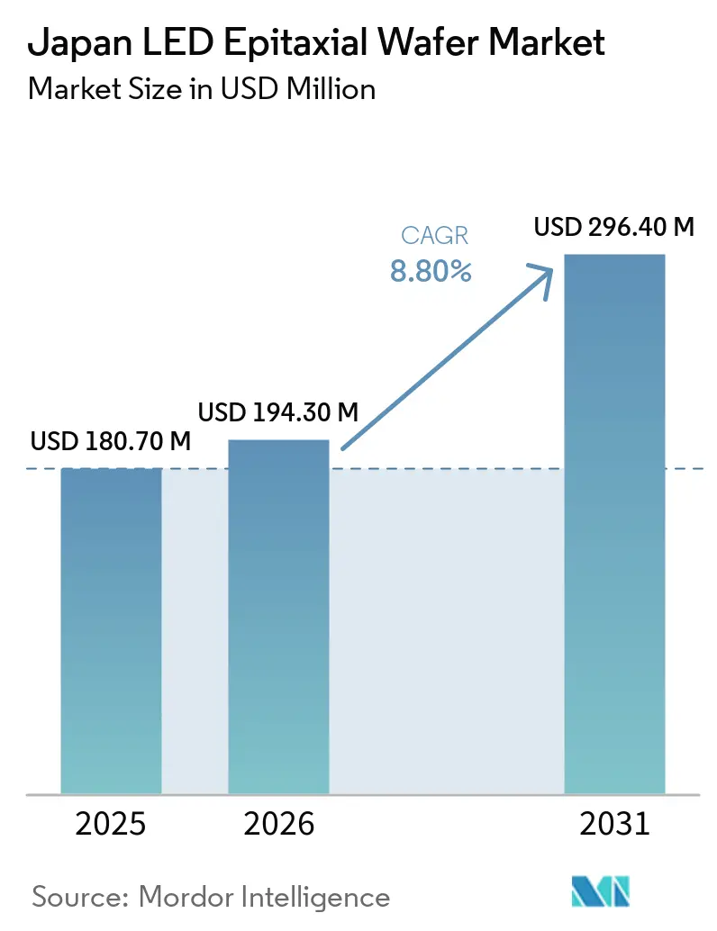
| Base Year Market Size (2025) | USD 180.70 Million |
| Market Size (2026) | USD 194.30 Million |
| Market Size (2031) | USD 296.40 Million |
| Growth Rate (2026 - 2031) | 8.80% CAGR |
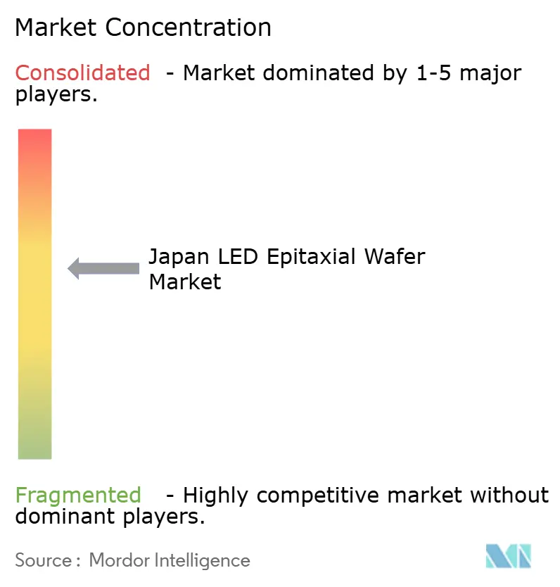
| Market Concentration | Medium |
Major Players *Disclaimer: Major Players sorted in no particular order Image © Mordor Intelligence. Reuse requires attribution under CC BY 4.0. | |
Japan LED Epitaxial Wafer Market Analysis by Mordor Intelligence
The Japan LED epitaxial wafer market size is expected to increase from USD 180.7 million in 2025 to USD 194.3 million in 2026 and reach USD 296.4 million by 2031, growing at an 8.80% CAGR over 2026-2031. Domestic suppliers have pivoted from commoditized white-LED volumes to premium wafers for automotive matrix headlamps, deep-UV sterilization units, and micro-LED backlights, where sub-nanometer uniformity commands higher pricing. Material-science strengths, notably the availability of ultra-high-purity metalorganic precursors, continue to differentiate the Japan LED epitaxial wafer market from lower-cost foreign competitors. Advancing commitments to 150 mm and 200 mm diameters reflect a drive for higher die counts per wafer despite the capital burden of next-generation MOCVD tools. Competition from Chinese foundries keeps average selling prices under pressure, yet long-term supply agreements with automotive and UV-device makers help stabilize cash flows for domestic producers.
Key Report Takeaways
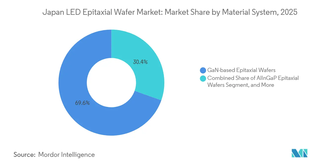
- By material system, GaN captured 69.60% of the Japan LED epitaxial wafer market share in 2025, while AlGaN is forecast to advance at a 12.50% CAGR through 2031.
- By substrate, sapphire accounted for 58.30% of the Japan LED epitaxial wafer market size in 2025, and silicon substrates are projected to expand at a 12.80% CAGR through 2031.
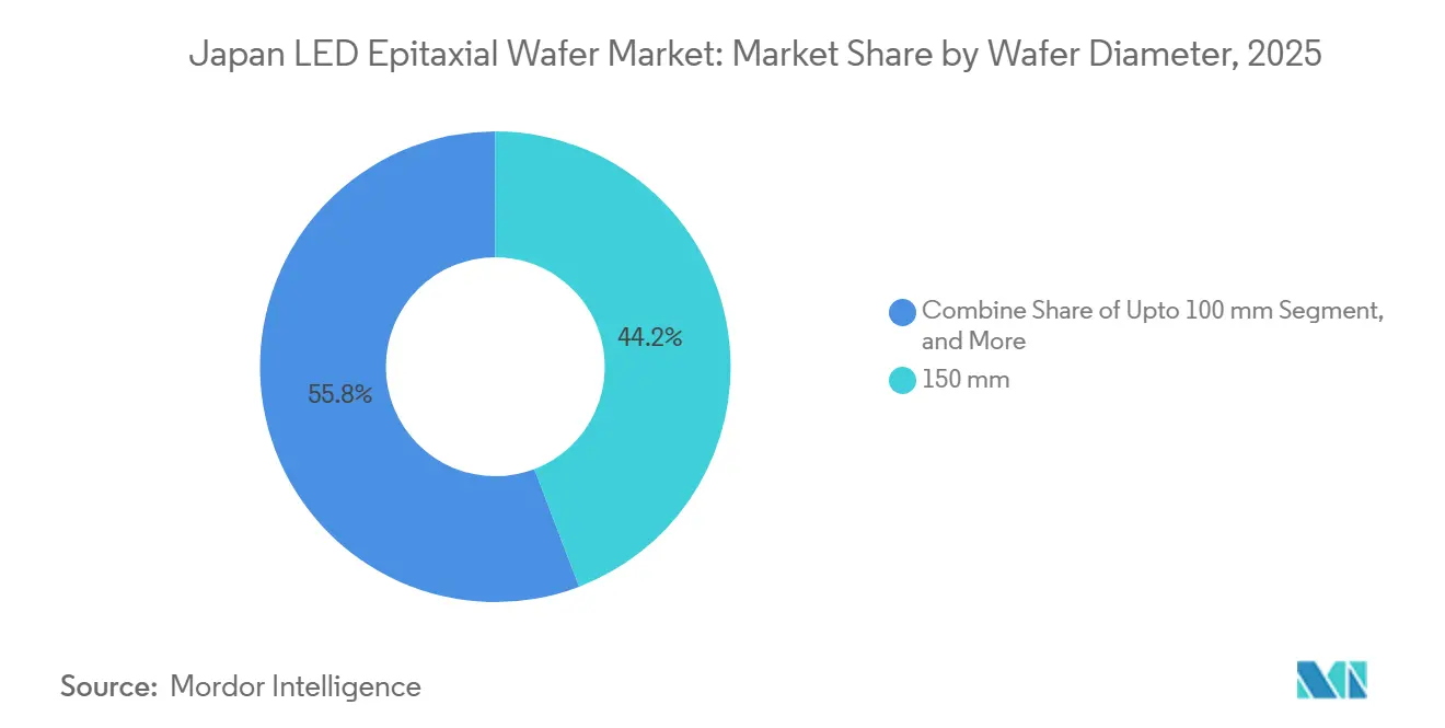
- By wafer diameter, 150 mm accounted for 44.20% of the Japan LED epitaxial wafer market in 2025, whereas 200 mm and above formats are expected to grow at a 13.20% CAGR through 2031.
- By application, general lighting accounted for 43.70% of 2025 revenue, and displays and backlighting are set to grow at a 13.50% CAGR through 2031.
Note: Market size and forecast figures in this report are generated using Mordor Intelligence’s proprietary estimation framework, updated with the latest available data and insights as of January 2026.
Japan LED Epitaxial Wafer Market Trends and Insights
Drivers Impact Analysis*
| DRIVER | (~) % IMPACT ON CAGR FORECAST | GEOGRAPHIC RELEVANCE | IMPACT TIMELINE |
|---|---|---|---|
| Intensifying Demand for High-Brightness LEDs in Automotive Headlamps | +2.3% | National clusters in Aichi and Shizuoka | Medium term (2-4 years) |
| Government Incentives for Domestic Compound-Semiconductor Production | +1.8% | National, led by METI subsidy programs | Long term (≥4 years) |
| Rapid Penetration of MiniLED Backlighting in High-End TVs | +1.5% | National with export spillovers | Short term (≤2 years) |
| Surge in UV-C LED Adoption for Sterilization Equipment | +1.4% | National, early uptake in healthcare and water utilities | Medium term (2-4 years) |
| Expansion of Smart Manufacturing Lines for MicroLED | +1.2% | Kyoto and Tokyo R&D hubs | Long term (≥4 years) |
| Emergence of GaN-on-Si Technology Partnerships with Foundries | +0.9% | Domestic with cross-border links | Medium term (2-4 years) |
| Source: Mordor Intelligence | |||
Intensifying Demand for High-Brightness LEDs In Automotive Headlamps
Adaptive matrix headlamps require epitaxial layers with sub-1% in-plane wavelength variation to prevent color shift across the beam. Nichia’s new automotive innovation center accelerates co-development cycles, giving Japanese suppliers early design-win opportunities.[1]Nichia Corporation, “Nichia Automotive Innovation Center Press Release,” ledinside.comTier-1 lamp makers validate domestic wafers against stringent PPAP tests, reinforcing long contracts that shield producers from commodity price swings. Silicon substrates improve thermal management inside compact headlamp housings. The growing pixel count per module lifts wafer demand despite price compression in conventional lighting diodes.
Government Incentives for Domestic Compound-Semiconductor Production
A JPY 101.7 billion (USD 0.64 billion) subsidy package, including JPY 70.5 billion (USD 0.44 billion) directed to SiC epi capacity, lowers capital hurdles for MOCVD line upgrades and broadens the precursor supply base. Shared infrastructure, such as bulk gas farms and clean-room expansions, indirectly benefits LED wafer fabs by cutting procurement lead times for NH₃ and TMGa. Policy continuity signals a long-range commitment that de-risks private investment in next-generation reactors and metrology.
Rapid Penetration of MiniLED Backlighting in High-End TVs
REGZA’s 116-inch RGB mini-LED model demonstrates domestic readiness for multi-color backlight architectures that require tightly binned epitaxial output.[2]TVS REGZA Corporation, “RGB Mini LED Television Launch,” regza.com Each television integrates thousands of discrete red, green, and blue chips, raising chip-per-wafer extraction ratios and pushing suppliers to improve die-level uniformity. Fast product cycles in consumer displays reward vertically integrated manufacturers that can iterate epi structures without third-party hand-offs. The short qualification horizon magnifies near-term demand growth.
Surge In UV-C LED Adoption for Sterilization Equipment
Nichia’s NCSU434D device achieves 7.4% wall-plug efficiency at 280 nm, a 2.5-fold increase from 2021, validating AlGaN wafers with low dislocation densities. Municipal water projects and hospital retrofits favor mercury-free solutions, locking in premium ASPs for wafers that deliver 25,000-hour lifetime targets. Research showing Mg-doping control extends life to 6,070 hours at 65 °C underpins confidence in long-term reliability. These performance milestones fortify Japan’s competitive advantage in deep-UV niches.
Restraints Impact Analysis*
| RESTRAINT | (~) % IMPACT ON CAGR FORECAST | GEOGRAPHIC RELEVANCE | IMPACT TIMELINE |
|---|---|---|---|
| High Capital Expenditure for New MOCVD Reactors | -1.6% | Nationwide, toughest on small fabs | Short term (≤2 years) |
| Supply Chain Disruptions for High-Purity Ammonia Gas | -1.1% | Nationwide gas networks | Medium term (2-4 years) |
| Competition from Low-Cost Chinese Epitaxy Suppliers | -0.9% | Domestic pricing pressure | Long term (≥4 years) |
| Limited Availability of 8-inch SiC Substrates | -0.7% | Global substrate shortage | Medium term (2-4 years) |
| Source: Mordor Intelligence | |||
High Capital Expenditure for New MOCVD Reactors
State-of-the-art MOCVD units cost USD 1.5-3 million each, and domestic plants must retrofit multi-chamber configurations with in-situ metrology, straining balance sheets just as LED ASPs decline.[3]Semiconductor Insight Research Team, “MOCVD Market 2026,” semiconductorinsight.com Nichia’s impairment of idle cathode tools illustrates the risk of misaligned capex. Smaller wafer houses lacking credit access face consolidation or exit. Equipment vendors’ pricing power further limits negotiation room for Japanese buyers.
Supply Chain Disruptions for High-Purity NH₃ Gas
Ultra-high-purity NH₃ (≥99.9999 %) is vital for GaN and AlGaN growth, yet geopolitical events and safety regulations have tightened supplies. On-site generation systems add infrastructure cost and raise compliance obligations under NFPA 55. While domestic gas firms pursue redundancy, additional purification steps raise consumable costs, which wafer makers struggle to pass through to price-sensitive customers.
*Our forecasts treat driver/restraint impacts as directional, not additive. The impact forecasts reflect baseline growth, mix effects, and variable interactions.
Segment Analysis
By Material System: AlGaN Ascends on UV Momentum
AlGaN’s share remains modest, but its projected 12.50% CAGR reflects heightened demand for sterilization and sensing devices that rely on deep-UV emission. The Japan LED epitaxial wafer market size for GaN remains dominant thanks to general lighting and automotive volumes, yet innovation energy is clearly shifting toward AlGaN, where lifetime gains secure premium margins. Research breakthroughs with 6-inch sapphire templates show only 1.6% variation in emission, confirming manufacturability at scale.[4]Yoshinaga et al., “Crack-Free UVC Growth on 6-Inch Sapphire,” spie.org
GaN maintains cost and defect-density advantages, but future revenue growth tilts toward AlGaN and niche AlInGaP. Emerging RGB color-conversion paths in micro-LED displays cap direct red AlInGaP demand. Consequently, the Japan LED epitaxial wafer market will likely bifurcate into a cost-sensitive GaN core and a high-margin AlGaN frontier catering to long-life UV applications.


By Substrate Type: Silicon’s Thermal Edge Strengthens Adoption
Sapphire’s 58.30% 2025 share underscores the inertia of established C-plane recipes and optical transparency. Nevertheless, silicon’s superior 150 W m⁻¹ K⁻¹ thermal conductivity and compatibility with existing CMOS lines underpin its projected 12.80% CAGR. Automotive headlamp modules that operate above 150 °C favor GaN-on-Si designs, a shift that enlarges silicon’s addressable slice of the Japan LED epitaxial wafer market.
Silicon carbide excels in heat removal at 490 W m⁻¹ K⁻¹, yet 8-inch wafer scarcity and elevated cost slow adoption. Gallium arsenide remains confined to specialty lasers. Consequently, sapphire holds volume leadership in mainstream LEDs, whereas silicon captures fast-growing segments that demand thermally robust, vertically structured chips.
By Wafer Diameter: 200 mm Migration Gains Pace
The 150 mm node balances reactor availability with manageable capex, but the 200 mm node is gaining ground as makers chase die-per-wafer efficiency. InnoGaN’s 8-inch ramp highlights the scale benefits that Japanese fabs must emulate or offset through specialization. Japan's LED epitaxial wafer market size growth is concentrated in the 200 mm tier, where per-die cost has fallen by more than 40%.
Domestic tool vendors are completing multi-chamber MOCVD platforms that maintain uniformity over larger surfaces. Smaller diameters remain important for R&D and low-volume custom runs, allowing niche producers to avoid direct cost wars with large Chinese competitors.
By Application: Displays And Backlighting Lead Growth
Mini-LED and micro-LED backlights are forecast to rise at a 13.50% CAGR, outpacing general lighting’s mature trajectory. Each 100-inch micro-LED television integrates tens of millions of chips, multiplying wafer demand despite yield challenges. Automotive cockpit displays add further pull for high-luminance, long-lifetime wafers.
General lighting stays the volume anchor thanks to retrofits in residential and commercial sectors, but price erosion compresses margins. UV sterilization uses fewer wafers but commands premiums due to tight wavelength and lifetime specifications. This mix positions displays, automotive, and UV segments as the profitability engines within the broader Japan LED epitaxial wafer market.
Geography Analysis
Regional demand clusters align with Japan’s industrial heartlands. Chubu, anchored by Aichi’s automotive ecosystem, accounts for a large share of high-brightness headlamp wafer orders as local tier-1 suppliers prefer proximate sources for just-in-time delivery. Kansai, with its concentration of display panel R&D, drives early adoption of mini-LED backlight wafers that require rapid design iteration.
Kanto’s electronics corridor houses multiple consumer-device assemblers that consume mid-power white LEDs and, increasingly, RGB mini-LED dies for notebooks and monitors. Tokushima and Kyushu host long-standing MOCVD fabs; proximity to research universities supports the Japan LED epitaxial wafer industry in pilot-scale AlGaN and GaN-on-GaN programs. Northern Tohoku leverages lower land and utility costs to attract greenfield 200 mm projects, though workforce availability remains a constraint.
Export considerations also shape regional dynamics. Ports in Osaka and Yokohama facilitate outbound logistics for high-value micro-LED wafers shipped to Taiwan and South Korea for final device integration. Meanwhile, interior regions such as Gifu and Nagano benefit from government grants that encourage the decentralization of sensitive compound semiconductor production away from seismic zones along the Pacific coast. Collectively, these geographic nuances influence investment timing and customer proximity strategies in the Japan LED epitaxial wafer market.
Competitive Landscape
The market is moderately fragmented. Nichia, Toyoda Gosei, and Resonac anchor domestic supply, while foreign rivals Sanan Optoelectronics and Epistar exert downward price pressure. Nichia’s JPY 60 billion miniLED capacity plan underscores a vertical-integration hedge that pairs epitaxy with in-house packaging. Toyoda Gosei’s Na-flux GaN crystal project aims to internalize large-diameter substrates, shortening supply chains for future UV and power devices.[5]Toyoda Gosei Co., “Toyoda Gosei Report 2024,” toyoda-gosei.com
Resonac positions itself as the world’s leading independent SiC epi supplier, using NEDO grants to pursue 8-inch defect cuts for late-decade volume. Chinese entrants offer 40% lower wafer pricing, leveraging scale economics and cheap electricity that remain difficult for Japanese firms to match.
However, stringent automotive lifetime requirements and export controls on deep-UV devices protect domestic specialty niches. Collective efforts to embed AI-driven process control and real-time metrology into MOCVD lines represent the next battleground for yield and cost leadership.
Japan LED Epitaxial Wafer Industry Leaders
Nichia Corporation
Toyoda Gosei Co., Ltd.
Coherent Corp.
Resonac Holdings Corporation
Sumitomo Electric Industries, Ltd.
- *Disclaimer: Major Players sorted in no particular order

Recent Industry Developments
- January 2026: Nichia expanded its mercury-free manufacturing initiative by replacing UV mercury lamps with UV-LED sources, cutting CO₂ emissions per light source by 35%.
- December 2025: REGZA launched Japan’s first RGB mini-LED television, a 116-inch model employing thousands of discrete red, green, and blue chips.
- January 2025: Pi Photonics secured Series C funding from Toyoda Gosei to accelerate development of highly directional industrial LED lighting.
- December 2024: METI approved a JPY 101.7 billion (USD 0.067 billion) subsidy for semiconductor materials, with Denso and Fuji Electric earmarked for large-scale SiC epi expansion.


Japan LED Epitaxial Wafer Market Report Scope
The Japan LED Epitaxial Wafer Market Report is Segmented by Material System (GaN-based, AlInGaP, and AlGaN), Substrate Type (Sapphire, Silicon, SiC, and GaAs), Wafer Diameter (Up to 100 mm, 150 mm, and 200 mm and Above), and Application (General Lighting, Automotive, Displays and Backlighting, UV Sterilization, and Industrial and Specialty). The Market Forecasts are Provided in Terms of Value (USD).
| GaN-based Epitaxial Wafers |
| AlInGaP Epitaxial Wafers |
| AlGaN Epitaxial Wafers |
| Sapphire |
| Silicon |
| Silicon Carbide (SiC) |
| Gallium Arsenide (GaAs) |
| Upto 100 mm |
| 150 mm |
| 200 mm and Above |
| General Lighting |
| Automotive Lighting |
| Displays and Backlighting |
| UV Sterilization |
| Industrial and Specialty Lighting |
| By Material System | GaN-based Epitaxial Wafers |
| AlInGaP Epitaxial Wafers | |
| AlGaN Epitaxial Wafers | |
| By Substrate Type | Sapphire |
| Silicon | |
| Silicon Carbide (SiC) | |
| Gallium Arsenide (GaAs) | |
| By Wafer Diameter | Upto 100 mm |
| 150 mm | |
| 200 mm and Above | |
| By Application | General Lighting |
| Automotive Lighting | |
| Displays and Backlighting | |
| UV Sterilization | |
| Industrial and Specialty Lighting |


Key Questions Answered in the Report
What is the 2026 market size of the Japan LED epitaxial wafer market?
The Japan LED epitaxial wafer market size is about USD 194.3 million in 2026, on a path to USD 296.4 million by 2031.
Which material system is growing the fastest?
AlGaN wafers post the fastest growth, advancing at roughly 12.50% CAGR to meet rising deep-UV LED demand.
Why are silicon substrates gaining share?
Silicon offers better thermal conductivity than sapphire and aligns with existing CMOS infrastructure, enabling cost-effective, vertically structured GaN devices.
What is driving the adoption of larger wafer diameters?
Moving to 200 mm and 8-inch formats increases chips per wafer, lowering unit costs and supporting high-volume applications such as mini-LED backlighting.
How are government incentives influencing domestic capacity?
METI subsidies reduce capital barriers for new MOCVD lines and substrate plants, strengthening onshore supply resilience.
Which end-use segment offers the highest growth potential?
Displays and backlighting, including mini-LED and micro-LED, are forecast to deliver the fastest revenue expansion through 2031.
Page last updated on:


