Japan Semiconductor Silicon Wafer Market Size and Share
Market Overview
| Study Period | 2020 - 2031 |
|---|---|
| Forecast Data Period | 2026 - 2031 |
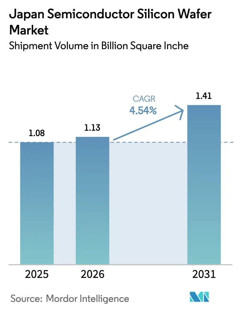
| Base Year Market Size (2025) | 1.08 Billion Square Inche |
| Market Volume (2026) | 1.13 Billion Square Inche |
| Market Volume (2031) | 1.41 Billion Square Inche |
| Growth Rate (2026 - 2031) | 4.54% CAGR |
| Market Concentration | High |
Major Players *Disclaimer: Major Players sorted in no particular order Image © Mordor Intelligence. Reuse requires attribution under CC BY 4.0. | |
Japan Semiconductor Silicon Wafer Market Analysis by Mordor Intelligence
The Japan Semiconductor Silicon Wafer Market size in terms of shipment volume is expected to increase from 1.08 Billion Square Inche in 2025 to 1.13 Billion Square Inche in 2026 and reach 1.41 Billion Square Inche by 2031, growing at a CAGR of 4.54% over 2026-2031.
Policy makers have placed upstream materials at the center of the country’s re-shoring push, tying multi-year subsidies to local wafer output, advanced packaging, and 2-nanometer logic readiness. Demand is clustering around 300 millimeter substrates as new logic and high-bandwidth memory lines ramp, while specialty silicon gains traction in automotive and radio-frequency designs. Large incumbents maintain scale advantages, yet rising power tariffs and strict wastewater rules compress margins and open niches for agile specialty-wafer suppliers. Talent shortages and smartphone cyclicality remain the main near-term brakes, but long-duration automotive contracts and domestic mega-fab expansions underpin the medium-term growth outlook for the Japan semiconductor silicon wafer market.
Key Report Takeaways
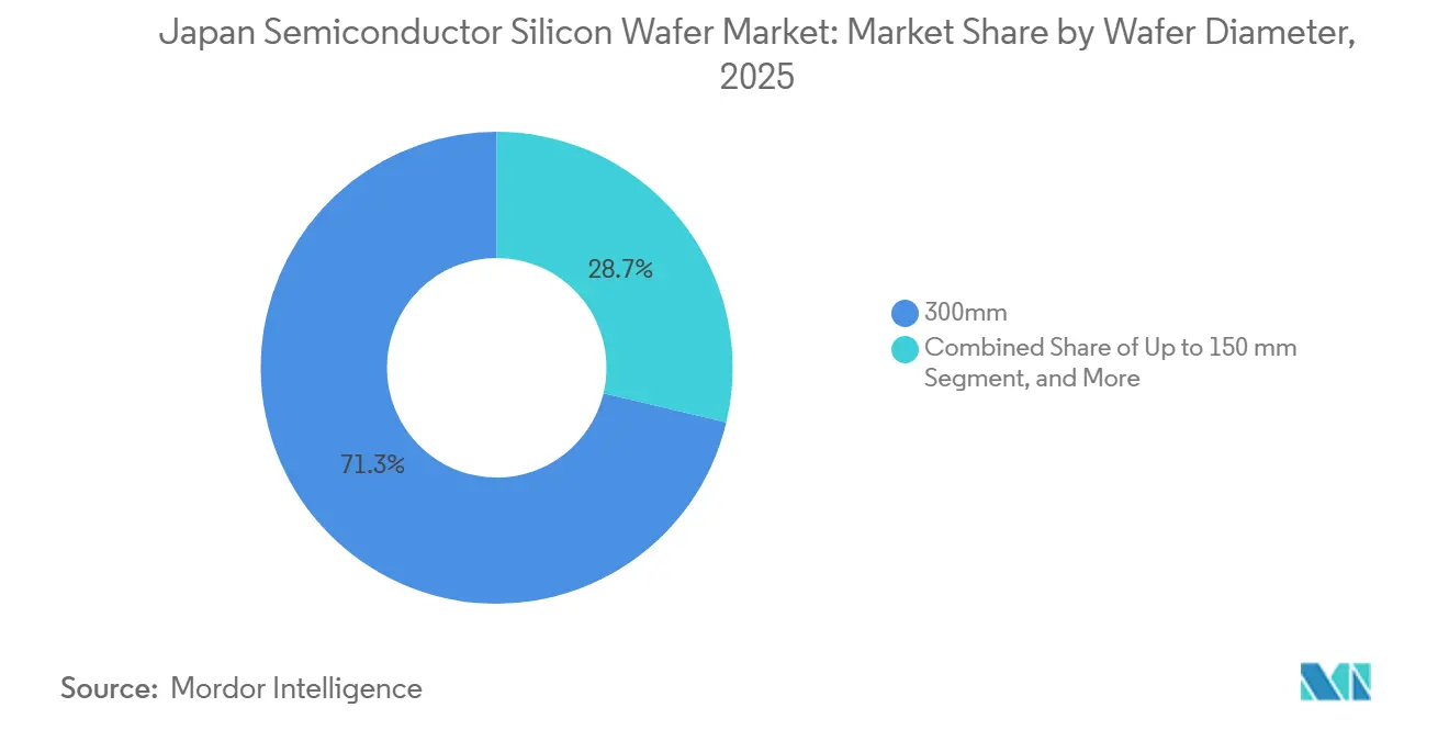
- By wafer diameter, the 300 millimeter category held 71.28% of Japan semiconductor silicon wafer market share in 2025 and is projected to expand at a 4.95% CAGR through 2031.
- By semiconductor device type, logic devices accounted for 36.29% of Japan semiconductor silicon wafer market share in 2025, while the same segment also leads growth at a 5.05% CAGR over 2026-2031.
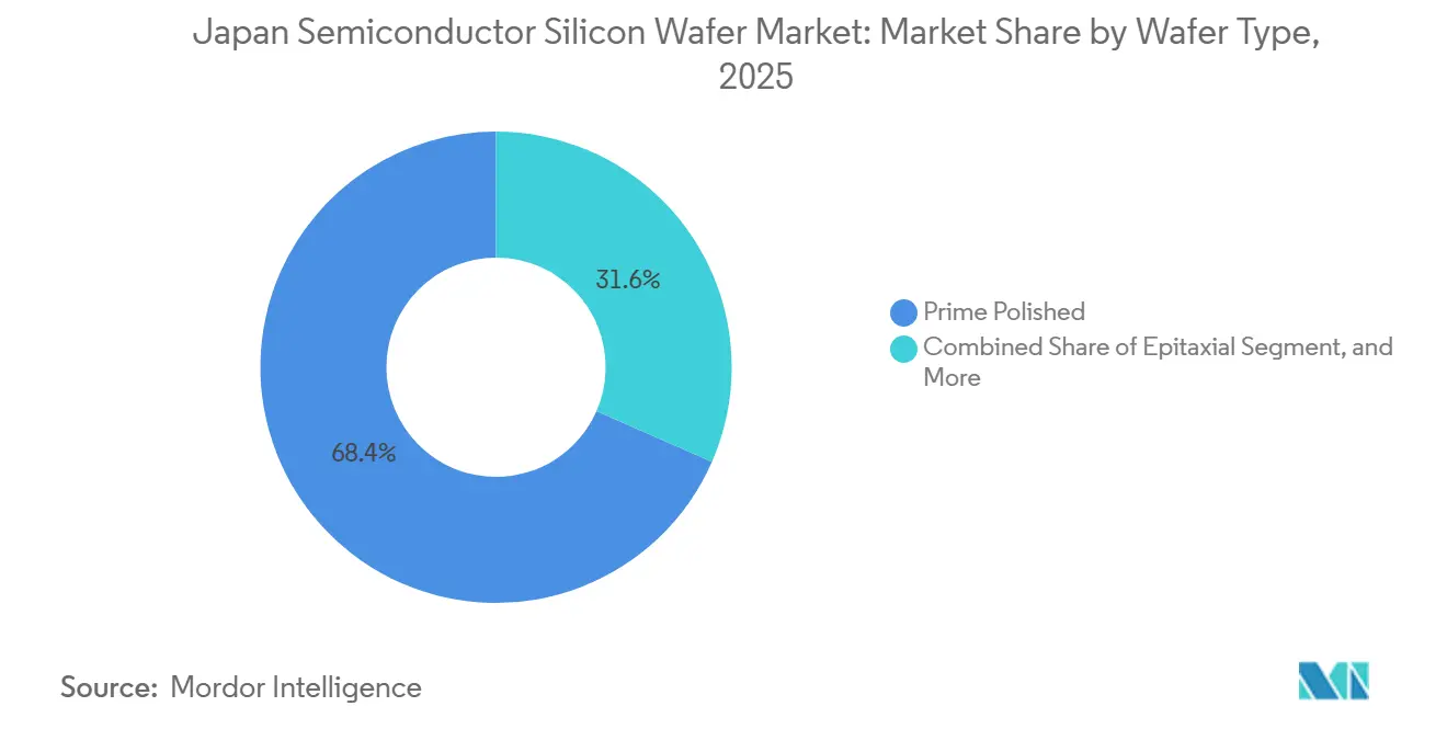
- By wafer type, prime polished substrates captured 68.44% share of the Japan semiconductor silicon wafer market size in 2025, whereas silicon-on-insulator wafers register the fastest 4.73% CAGR to 2031.
- By end user, consumer electronics represented 39.64% of Japan semiconductor silicon wafer market share in 2025, but automotive applications are advancing at a 5.09% CAGR and outpace every other category during the forecast period.
Note: Market size and forecast figures in this report are generated using Mordor Intelligence’s proprietary estimation framework, updated with the latest available data and insights as of January 2026.
Japan operates as part of an interconnected international environment rather than as a self-contained country level unit. The semiconductor silicon wafer market research by Mordor Intelligence places together all major developments across the globe within that wider frame.
Japan Semiconductor Silicon Wafer Market Trends and Insights
Drivers Impact Analysis*
| Driver | (~) % Impact on CAGR Forecast | Geographic Relevance | Impact Timeline |
|---|---|---|---|
| Rising Demand for 300 mm Wafers in Logic and Memory Devices | +1.2% | National, Kumamoto and Hokkaido Clusters | Medium Term (2–4 Years) |
| Government Subsidies for Domestic Wafer Capacity Expansion | +1.0% | National, Kyushu and Tohoku | Short Term (≤2 Years) |
| Kumamoto Mega-Fab Build-Out by TSMC-Sony JV | +0.9% | National, Kyushu Supply Chain | Medium Term (2–4 Years) |
| Accelerated Electrification of Japanese Automotive Industry | +0.7% | National, Toyota City and Yokohama Corridors | Long Term (≥4 Years) |
| Supply-Chain Re-Shoring Initiatives Among IDMs | +0.5% | National, Renesas and Rohm Sites | Medium Term (2–4 Years) |
| Breakthrough in Float-Zone-Czochralski Hybrid Crystal Pulling | +0.3% | National, Shin-Etsu and SUMCO R&D Sites | Long Term (≥4 Years) |
| Source: Mordor Intelligence | |||
Rising Demand For 300 mm Wafers In Logic And Memory Devices
Shipments of 300-millimeter substrates grew 5.8% year on year in 2025 as artificial-intelligence accelerators and sub-16-nanometer logic scaled up volume.[1]SEMI, “300 mm Silicon Wafer Shipment Report 2025,” semi.org The first Kumamoto line alone pulls roughly 55,000 wafers each month, and its phase-two expansion adds another 50,000 by late 2027, lifting domestic demand by more than 1.2 million wafers annually. Parallel node migrations in DRAM and NAND eliminate the cost advantage of 200 millimeter tools, intensifying the swing toward larger diameters. Crystal-growth equipment lead times hover at 18 months, delaying supply responses and preserving tight market conditions. This driver, therefore, anchors mid-term growth for the Japan semiconductor silicon wafer market.
Government Subsidies For Domestic Wafer Capacity Expansion
The Ministry of Economy, Trade and Industry budgeted JPY 1.23 trillion (USD 8.7 billion) for semiconductor infrastructure in fiscal 2026, with JPY 400 billion (USD 2.8 billion) ring-fenced for wafer lines, epitaxial tools, and materials R and D.[2]Ministry of Economy Trade and Industry, “FY2026 Budget for Semiconductor Infrastructure,” meti.go.jp Funding agreements oblige suppliers to hit domestic employment and technology-transfer targets, ensuring near-term installation of an additional 300 millimeter pullers and epitaxial reactors. Shin-Etsu and SUMCO together secured JPY 95 billion (USD 670 million) to lift capacity by 15% through 2027, while midsize firms accessed smaller grants for specialty silicon. The front-loaded nature of disbursements gives the Japan semiconductor silicon wafer market an immediate volume boost and offsets the capital intensity of environmental compliance.
Kumamoto Mega-Fab Build-out By TSMC-Sony JV
Mass production began in December 2024 and reached 40,000 wafers per month by March 2025. An upgrade announced in February 2026 moves the second facility to a 3-nanometer node and raises total capex to USD 12 billion, locking in an additional pull of 50,000 300-millimeter wafers monthly from late 2027.[3]Bloomberg, “TSMC Upgrades Kumamoto Project to 3 nm,” bloomberg.com 95% of these substrates are sourced domestically, securing off-take for local wafer makers and catalyzing the establishment of more than 40 supplier offices across Kyushu. The cluster effect reduces logistics overhead, spurs university training programs, and entrenches the fab as a medium-term demand pillar.
Accelerated Electrification Of Japanese Automotive Industry
Electrified vehicles accounted for 38% of domestic output in 2025, tripling chip content per car compared with combustion models. Tier-ones such as DENSO are committed to local sourcing of 200-millimeter silicon carbide wafers by 2027, redirecting USD 300 million in annual purchases to Japanese vendors and trimming lead times by half. Battery-electric platforms integrate high-voltage inverters, battery-management ICs, and advanced driver-assistance sensors, all of which pull incremental wafer area. Because automotive programs run on multi-year contracts, they buffer the Japan semiconductor silicon wafer market from consumer-electronics volatility and underpin long-term capacity investments.
Restraints Impact Analysis*
| Restraint | (~) % Impact on CAGR Forecast | Geographic Relevance | Impact Timeline |
|---|---|---|---|
| Prolonged Downturn in Global Smartphone Demand | −0.8% | Global Exports to Taiwan and China | Short Term (≤2 Years) |
| High Electricity Costs Affecting Manufacturing Competitiveness | −0.6% | National, Kansai and Chubu Grids | Medium Term (2–4 Years) |
| Stringent Waste-Water Regulations on Silicon Processing | −0.3% | National, Pre-2010 Facilities | Long Term (≥4 Years) |
| Engineering Talent Shortage in Crystal Growth Operations | −0.5% | National, Kyushu and Tohoku | Medium Term (2–4 Years) |
| Source: Mordor Intelligence | |||
Prolonged Downturn In Global Smartphone Demand
Three consecutive quarters of shipment contraction in early 2025 cut high-margin logic-wafer exports to overseas foundries. Shin-Etsu idled two pullers and deferred a JPY 30 billion (USD 210 million) expansion, while SUMCO trimmed revenue guidance by 7% . Because smartphone processors and NAND controllers require tight flatness and low contamination, the lost orders carry outsized profitability. Recovery hinges on 5 G penetration in price-sensitive markets, leaving a near-term hole in utilization rates for the Japan semiconductor silicon wafer market.
High Electricity Costs Affecting Manufacturing Competitiveness
Industrial tariffs averaged JPY 18.5 per kilowatt-hour (USD 0.13) in 2025, roughly 30% above South Korea and 25% above Taiwan.[4]Ministry of the Environment, “Fluoride Effluent Standards for Semiconductor Plants,” env.go.jp A single 300-millimeter wafer consumes about 200 kilowatt-hours, creating an electricity penalty of about JPY 860 (USD 6) per wafer versus Korean peers. Large producers hedge through power purchase agreements, while midsize fabs in Kansai and Chubu face thinner margins and tougher upgrade decisions. Elevated energy costs therefore squeeze reinvestment budgets and curb incremental capacity, constraining medium-term growth.
*Our forecasts treat driver/restraint impacts as directional, not additive. The impact forecasts reflect baseline growth, mix effects, and variable interactions.
Segment Analysis
By Wafer Diameter: 300 mm Capacity Tightens As Legacy Nodes Stabilize
The 300 millimeter category dominated the Japan semiconductor silicon wafer market size with a 71.28% volume share in 2025 and continues to outgrow smaller diameters at a 4.95% CAGR. Node migrations below 16 nanometers and high-bandwidth memory stacking make large-area substrates essential for cost amortization, and the Kumamoto and Hokkaido fabs together will require more than 2 million wafers annually by 2028. Tight supply directs capital toward new Czochralski pullers and advanced polishing lines, yet 18-month tool lead times delay relief until mid-2027.
Conversely, the 200 millimeter segment retains an entrenched role in analog, power and microcontroller production that favors proven process recipes over die density. Automotive electrification, industrial automation and sensor demand keep 200 millimeter fabs running near full utilization, even as equipment suppliers wind down spare-parts support. Diameters up to 150 millimeters remain niche at roughly 5% of volume, serving prototyping and specialty RF devices where quick cycle times trump economies of scale. This mixed outlook means the Japan semiconductor silicon wafer market share for 300 millimeter substrates will keep inching upward, while volumes for smaller diameters hold steady rather than fall.


By Semiconductor Device Type: Logic Leads While Power Devices Gain Momentum
Logic devices captured 36.29% of Japan's semiconductor silicon wafer market share in 2025, with expansion set at a 5.05% CAGR as 3-nanometer production localizes. Rapidus adds diversification by introducing 2-nanometer capacity in Hokkaido after 2027, anchoring additional wafer pull in northern Japan. Memory follows at 4.6% CAGR, buoyed by artificial-intelligence servers that integrate high-bandwidth DRAM stacks and dense NAND for edge storage.
Analog demand grows steadily across multi-year industrial and telecom design cycles, whereas discrete devices pivot toward silicon carbide and gallium nitride for high-voltage automotive inverters. Specialty categories such as sensors and optoelectronics accelerate alongside lidar and time-of-flight adoption in advanced driver-assistance systems. This balanced mix cushions the Japan semiconductor silicon wafer market against single-segment shocks and underscores the strategic value of maintaining breadth across device families.
By Wafer Type: Prime Polished Dominates, SOI Outpaces All Rivals
Prime polished substrates held 68.44% of volume in 2025 and, despite a slower 4.4% CAGR, remain the workhorse for logic, memory and standard analog parts. Scale efficiencies and long-term purchase agreements lock in capacity for flagship fabs, giving incumbents pronounced bargaining power.
Epitaxial wafers represent 22% of output and grow in line with overall demand, driven by power-device and RF designs that rely on controlled doping and defect-free layers. Silicon-on-insulator registers the fastest 4.73% CAGR as automotive microcontroller and RF front-end makers trade higher cost for lower leakage and improved thermal isolation. Specialty silicon, spanning high-resistivity and sensor-grade formats, continues to attract new entrants that differentiate through rapid customization. The widening gap between commodity and specialty wafers forces suppliers to reassess portfolio mixes and fosters innovation that ultimately benefits the Japan semiconductor silicon wafer market.
By End User: Automotive Surges As Consumer Electronics Matures
Consumer electronics retained the largest 39.64% share in 2025, yet its 3.9% CAGR lags the headline number because smartphones have reached unit saturation in developed economies. Wearables and smart-home products add incremental wafer volume, but not enough to offset sluggish flagship phone output.
Automotive applications post the swiftest 5.09% CAGR as electrified platforms embed semiconductor content up to 3 times that of combustion vehicles. Domestic sourcing mandates by DENSO and others strengthen the pull on local 200- and 300-millimeter lines, shortening supply chains and insulating demand from consumer cycles. PCs, servers, industrial automation and telecom infrastructure each grow near the market average, distributing risk across multiple verticals and stabilizing the Japan semiconductor silicon wafer market size trajectory.
Geography Analysis
Kyushu accounts for roughly 45% of domestic wafer consumption in 2026, fuelled by the Kumamoto mega-fab and a flock of supplier facilities that cut logistics costs by co-locating. The Kansai-Chubu corridor still hosts the largest crystal-growth plants, yet higher power tariffs and aging grids erode its cost edge. Hokkaido emerges as a strategic hub with the Rapidus 2 nanometer project, leveraging abundant hydroelectric capacity priced 15% below the national average and targeting 40,000 wafers per month of steady pull by 2029.
METI intentionally disperses subsidies so that no prefecture exceeds 50% of installed capacity by 2030, spreading economic gains and disaster risk. This policy leads to wafer trucking from Kansai to Kyushu that adds JPY 200-300 (USD 1.4-2.1) per substrate but builds national resilience. The Tohoku region plays a research-oriented role, supporting specialty silicon pilots near university labs and government prototyping centers.
Externally, 28% of polished-wafer exports ship to Taiwan and South Korea, linking Japan’s performance to the health of overseas foundries. The local TSMC line partly offsets that exposure by internalizing more than 1 million wafers annually, though it concentrates customer risk in two dominant suppliers. Southeast Asia presents a modest growth avenue for 200 millimeter demand, yet price-aggressive Chinese competitors dilute the opportunity. This geographic mosaic positions the Japan semiconductor silicon wafer market for steady growth while hedging against regional disruptions.
The semiconductor silicon wafer market is assessed by Mordor Intelligence through a multi-layered geographic lens, covering other regions such as Europe, North America, and Asia, along with detailed country-level analysis for China, South Korea, Germany, United States, Taiwan, and India.
Competitive Landscape
Shin-Etsu Chemical and SUMCO Corporation together command just over half of the domestic 300 millimeter output, giving the market an oligopolistic profile. Their scale enables investments in extreme flatness polishing and wastewater recycling, yet dependence on smartphones and memory cycles exposes earnings to demand swings. Smaller rivals such as GlobalWafers Japan, Siltronic and SK Siltron carve out share in epitaxial, SOI and high-resistivity niches where agility matters more than volume.
Chinese entrants offer 15-25% lower prices but higher defect densities, limiting penetration to non-critical applications. Intellectual property barriers in silicon-carbide, SOI bonding and ultra-high-resistivity substrates give established specialty players defensible moats. Environmental rules that cap fluoride discharge below 10 parts-per-million add JPY 2-5 billion (USD 14-35 million) in capital per fab, a hurdle that favors incumbents who can amortize upgrades across larger volumes.
Technology race dynamics intensify as device makers demand sub-0.3 micrometer thickness variation and nanotopography control tighter than 50 nanometers for extreme-ultraviolet compatibility. Shin-Etsu’s dozen patents on hybrid crystal pulling hint at a cost breakthrough that could tilt share further toward the leading duo. Meanwhile, labor shortages force all vendors to broaden apprenticeship pipelines, extending time-to-yield on new lines and leaving room for specialty entrants to win orders that hinge on close engineering collaboration within Japan semiconductor silicon wafer industry clusters.
Japan Semiconductor Silicon Wafer Industry Leaders
Shin-Etsu Chemical Co., Ltd.
SUMCO Corporation
GlobalWafers Japan Co., Ltd.
Siltronic AG
SK Siltron Co., Ltd.
- *Disclaimer: Major Players sorted in no particular order

Recent Industry Developments
- February 2026: TSMC raised investment for its second Kumamoto fab to USD 12 billion, upgraded the node to 3 nanometer and set late-2027 for production start-up, raising monthly wafer demand by 50,000.
- January 2026: METI approved a JPY 1.23 trillion (USD 8.7 billion) semiconductor package for fiscal 2026, earmarking JPY 400 billion (USD 2.8 billion) for wafer-substrate capacity and R&D.
- October 2025: GlobalWafers Japan started pilot production of fully depleted silicon-on-insulator wafers at a newly converted 200 millimeter line in Hokkaido, targeting 20,000 wafers per year for automotive microcontroller and RF front-end evaluations.
- November 2025: The Ministry of Economy, Trade and Industry introduced a 15% tax credit on capital invested in float-zone-Czochralski hybrid crystal-pulling tools ordered between November 2025 and March 2027, aiming to accelerate deployment of next-generation 300 millimeter ingot furnaces.


Japan Semiconductor Silicon Wafer Market Report Scope
The Japan Semiconductor Silicon Wafer Market Report is Segmented by Wafer Diameter (Up to 150 mm, 200 mm, 300 mm), Semiconductor Device Type (Logic, Memory, Analog, Discrete, Other), Wafer Type (Prime Polished, Epitaxial, SOI, Specialty Silicon), End-User (Consumer Electronics, Mobile and Smartphones, PCs and Servers, Industrial, Telecommunications, Automotive, Other), and Geography (Japan). Market Forecasts are Provided in Terms of Volume (Million Square Inches).
| Up to 150 mm |
| 200 mm |
| 300 mm |
| Logic |
| Memory |
| Analog |
| Discrete |
| Other Semiconductor Device Types (Optoelectronics, Sensors, Micro) |
| Prime Polished |
| Epitaxial |
| Silicon-on-Insulator (SOI) |
| Specialty Silicon (High-Resistivity, Power, Sensor-Grade) |
| Consumer Electronics |
| Mobile and Smartphones |
| PCs and Servers |
| Industrial |
| Telecommunications |
| Automotive |
| Other End-User |
| By Wafer Diameter | Up to 150 mm |
| 200 mm | |
| 300 mm | |
| By Semiconductor Device Type | Logic |
| Memory | |
| Analog | |
| Discrete | |
| Other Semiconductor Device Types (Optoelectronics, Sensors, Micro) | |
| By Wafer Type | Prime Polished |
| Epitaxial | |
| Silicon-on-Insulator (SOI) | |
| Specialty Silicon (High-Resistivity, Power, Sensor-Grade) | |
| By End-User | Consumer Electronics |
| Mobile and Smartphones | |
| PCs and Servers | |
| Industrial | |
| Telecommunications | |
| Automotive | |
| Other End-User |


Key Questions Answered in the Report
How large will the Japan semiconductor silicon wafer market be by 2031?
It is forecast to reach 1,406.42 million square inches by 2031, expanding at a 4.54% CAGR from 2026.
Which wafer diameter captures the majority of domestic demand?
300 millimeter substrates commanded 71.28% volume share in 2025 and continue to lead expansion through 2031.
What segment is growing fastest by end user?
Automotive applications post the highest 5.09% CAGR as electrification multiplies semiconductor content per vehicle.
How are government incentives influencing supply?
METI’s JPY 1.23 trillion FY 2026 package, including JPY 400 billion for wafer capacity, accelerates near-term installations and anchors local demand.
Which companies dominate the Japanese wafer landscape?
Shin-Etsu Chemical and SUMCO Corporation together supply just over half of domestic 300 millimeter output, while GlobalWafers Japan and others focus on specialty niches.
What is the main cost headwind for domestic wafer fabs?
Industrial electricity tariffs run roughly 30% higher than in South Korea, adding about JPY 860 in power cost per 300 millimeter wafer.
Page last updated on:


