Taiwan Semiconductor Silicon Wafer Market Size and Share
Market Overview
| Study Period | 2020 - 2031 |
|---|---|
| Forecast Data Period | 2026 - 2031 |
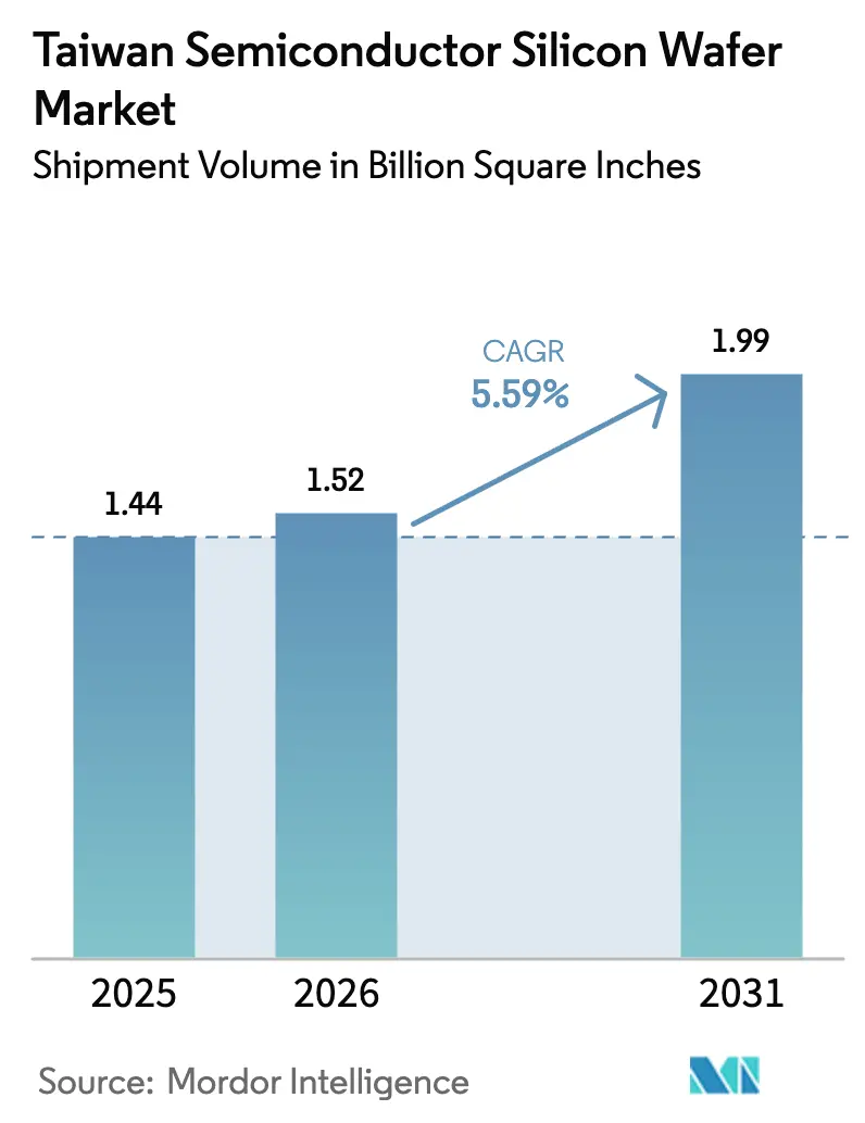
| Base Year Market Size (2025) | 1.44 Billion Square Inches |
| Market Volume (2026) | 1.52 Billion Square Inches |
| Market Volume (2031) | 1.99 Billion Square Inches |
| Growth Rate (2026 - 2031) | 5.59% CAGR |
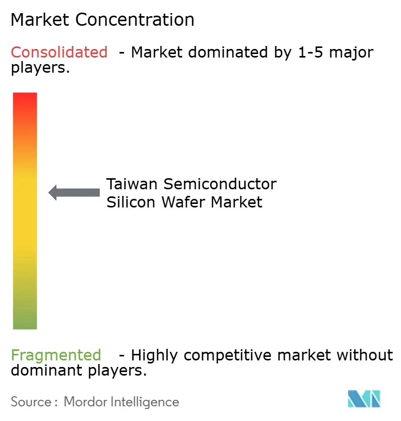
| Market Concentration | Medium |
Major Players *Disclaimer: Major Players sorted in no particular order Image © Mordor Intelligence. Reuse requires attribution under CC BY 4.0. | |
Taiwan Semiconductor Silicon Wafer Market Analysis by Mordor Intelligence
The Taiwan semiconductor silicon wafer market size is projected to be 1.44 billion square inches in 2025, 1.52 billion square inches in 2026, and reach 1.99 billion square inches by 2031, growing at a CAGR of 5.59% from 2026 to 2031. Record demand for 3-nanometer logic, the 2026 ramp of 2-nanometer nodes, and the steady retirement of 200 mm lines anchor this trajectory. Taiwan’s foundries absorbed more than seven-tenths of total wafer volume on 300 mm substrates in 2025, and multi-year volume contracts are locking in that dominance. Joint public-private spending of USD 250 billion under the 2026 United States–Taiwan Silicon Pact signals that geopolitics now shapes substrate allocations alongside Moore’s Law economics. Meanwhile, consumer electronics shipments stabilized, electric-vehicle silicon demand accelerated, and localized recycling infrastructure curbed virgin-wafer purchases, reinforcing Taiwan’s central role in global supply.
Key Report Takeaways
- By wafer diameter, 300 mm substrates led with 71.22% of the Taiwan semiconductor silicon wafer market share in 2025, while their volume is forecast to expand at a 6.01% CAGR through 2031.
- By semiconductor device type, logic devices captured 34.76% of the Taiwan semiconductor silicon wafer market size in 2025 and are projected to grow at a 6.22% CAGR to 2031.
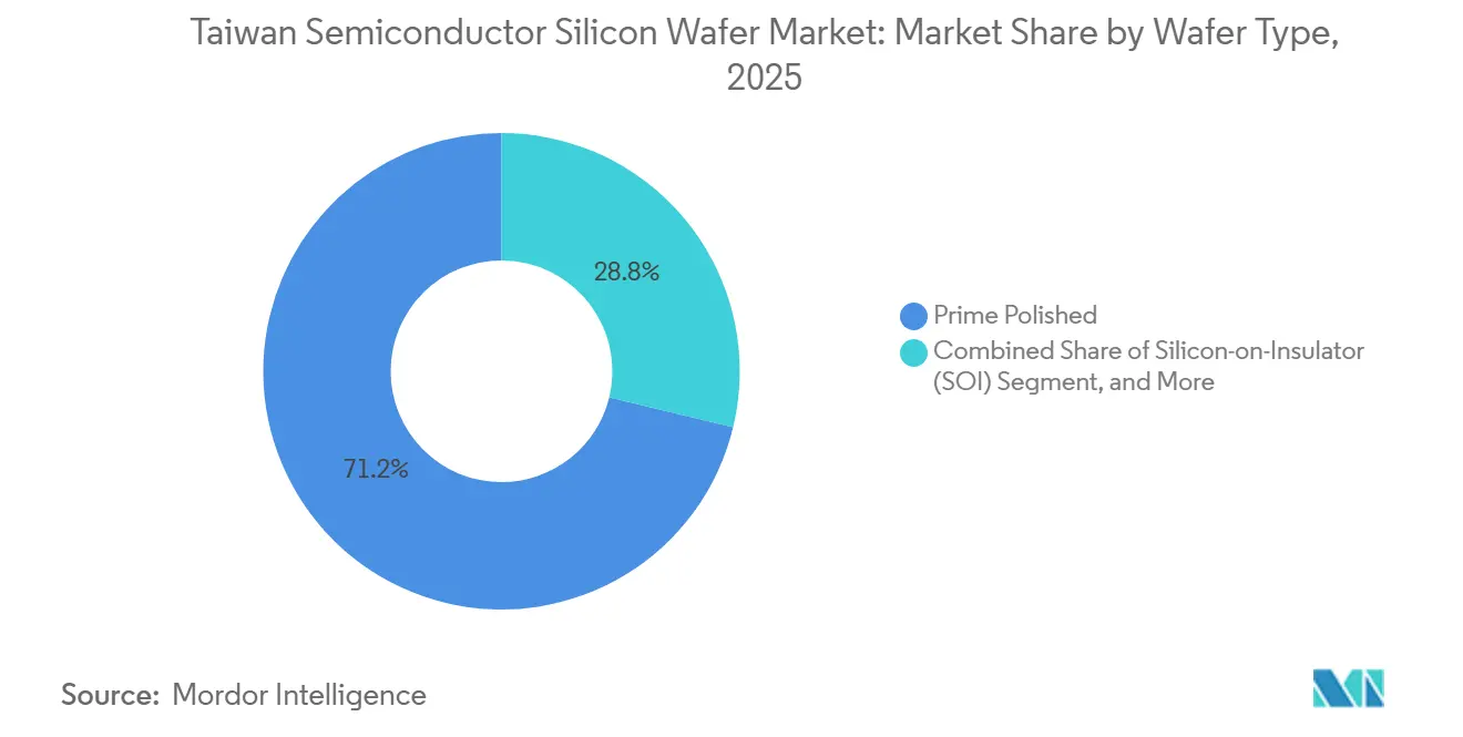
- By wafer type, prime polished held 71.22% revenue share in 2025; silicon-on-insulator substrates post the fastest growth at a 5.99% CAGR during 2026-2031.
- By end-user, consumer electronics commanded 41.11% of 2025 volume, while automotive applications record the highest projected CAGR at 6.33% through 2031.
Note: Market size and forecast figures in this report are generated using Mordor Intelligence’s proprietary estimation framework, updated with the latest available data and insights as of January 2026.
Proportional positioning is established by comparing country level and regional contributions against the global total, including that of Taiwan. The semiconductor silicon wafer market share in our global report expresses these relative weights.
Taiwan Semiconductor Silicon Wafer Market Trends and Insights
Drivers Impact Analysis*
| Driver | (~) % Impact on CAGR Forecast | Geographic Relevance | Impact Timeline |
|---|---|---|---|
| Expansion of 3nm and Below Process Node Capacity | +1.8% | Taiwan (Hsinchu, Tainan), with spillover to Arizona and Kumamoto fabs | Medium term (2-4 years) |
| Rising Demand for Power Electronics in EV Supply Chain | +1.2% | Global, with concentration in Taiwan supply base for Tier-1 automotive OEMs | Medium term (2-4 years) |
| Government Incentives under Taiwan Chips Act | +0.9% | Taiwan national, with early gains in Hsinchu Science Park and Southern Taiwan Science Park | Short term (≤ 2 years) |
| Adoption of 3DIC and Advanced Packaging Requiring Ultra-Thin Wafers | +0.7% | Taiwan (TSMC CoWoS lines), Japan (Amkor), and Arizona (Intel) | Medium term (2-4 years) |
| Emergence of Smart Manufacturing for Wafer Defect Reduction | +0.4% | Taiwan core fabs, expanding to Southeast Asia and United States greenfield sites | Long term (≥ 4 years) |
| Localization of Recycled Silicon Wafer Supply | +0.3% | Taiwan national, with pilot programs in Hsinchu and Tainan clusters | Long term (≥ 4 years) |
| Source: Mordor Intelligence | |||
Expansion Of 3 nm And Below Process Node Capacity
Taiwan Semiconductor Manufacturing Company operated its 3 nm lines at full utilization throughout 2025 and began 2 nm mass production in early 2026, after allocating USD 52 billion–USD 56 billion to EUV tools and cleanroom builds. Each 3 nm wafer demands epitaxial layers thinner than 2 µm, and defect budgets fall below 0.01 particles cm-², so suppliers installed atomic-layer deposition and advanced CMP systems that cost more than USD 100 million per tool.[1]Applied Materials Engineers, “SEMVision G10 Defect Inspection Platform Specifications,” Applied Materials, appliedmaterials.com Gate-all-around structures at 2 nm further double epitaxial cycles over 5 nm finFETs. With Taiwan holding more than half of global advanced-node capacity in 2025, multi-year wafer contracts exceeding 1 million units per customer underpin stable pricing.
Rising Demand For Power Electronics In EV Supply Chain
Electric-vehicle platforms shifted from 650 V to 800 V architectures during 2024-2025, lifting silicon-carbide substrate consumption per car by 60%. Automotive Tier-1s source their discrete power wafers from the same Taiwan foundries that fabricate microcontrollers, enabling consolidated audits. Wafer Works derived approximately half of 2024 revenue from epitaxial products and started qualifying GaN-on-Si wafers for 48 V hybrids in late 2025.[2]Wafer Works Corporation, “2024 Annual Report,” waferworks.com.tw United Microelectronics Corporation lifted the 8-inch power capacity by 15% in 2025, and Vanguard intends to convert a legacy 6-inch line to 8-inch SiC in 2026.[3]United Microelectronics Corporation, “Hsinchu Silicon Reclaim Center,” umc.com
Government Incentives Under Taiwan Chips Act
The January 2026 United States–Taiwan Silicon Pact earmarks USD 250 billion for joint semiconductor projects, with about 40% directed to wafer substrates and packaging. Taiwan’s Ministry of Economic Affairs now allows 25% tax credits for 300 mm fab capex and accelerates environmental permit approvals. GlobalWafers tapped these benefits to fast-track its Texas Phase 2 expansion and break ground on a EUR 2 billion (USD 2.16 billion) plant in Italy. Regulatory influence extends to export licensing. Taiwan added Huawei Technologies and Semiconductor Manufacturing International Corporation to its restricted-entity list in June 2025, aligning with United States controls and ensuring that advanced wafer substrates do not flow to Chinese fabs pursuing sub-7-nanometer nodes.
Adoption Of 3DIC And Advanced Packaging Requiring Ultra-Thin Wafers
Taiwan Semiconductor Manufacturing Company targets 130,000 CoWoS wafers per month by late 2026, a 160% jump over 2024. Interposer wafers are ground to 50 µm, increasing the risk of cracks unless laser grinding and plasma dicing are used. Silicon-on-insulator substrates simplify thinning because the buried oxide layer acts as an etch stop, enabling final thicknesses below 30 µm for RF and low-power dies. GlobalWafers’ Missouri SOI line, opened in 2025, will ship 200,000 wafers annually by 2027 under two U.S. fabless supply deals. Only four firms consistently meet the 100 nm TTV spec required for 3DIC hybrid bonding, reinforcing supplier concentration.
Restraints Impact Analysis*
| Restraint | (~) % Impact on CAGR Forecast | Geographic Relevance | Impact Timeline |
|---|---|---|---|
| Volatility in Polysilicon Prices | -0.6% | Global, with acute exposure in Taiwan and Japan wafer supply base | Short term (≤ 2 years) |
| High Capital Intensity and Long Payback Periods | -0.8% | Global, particularly acute for new entrants in Europe and United States | Long term (≥ 4 years) |
| Water Scarcity Risks in Hsinchu and Tainan Clusters | -0.5% | Taiwan national, concentrated in Hsinchu Science Park and Southern Taiwan Science Park | Medium term (2-4 years) |
| Geopolitical Tensions Impacting Equipment Imports | -0.4% | Taiwan national, with secondary effects on Japan and South Korea wafer suppliers | Short term (≤ 2 years) |
| Source: Mordor Intelligence | |||
Volatility In Polysilicon Prices
Spot prices for semiconductor-grade polysilicon ranged from USD 18 kg to USD 26 kg in 2025 as photovoltaic oversupply met refinery cutbacks. Sumco cited the swings when announcing the closure of its Miyazaki 200 mm line by 2026 to consolidate volume under more predictable feedstock deals with Tokuyama and Wacker. A single Wacker outage in Germany in 2024 removed 8% of global supply and lifted prices 22% in six weeks. GlobalWafers mitigates exposure through minority stakes in polysilicon ventures and in-house crystal pulling, yet smaller Taiwan players face margin compression during spikes.
High Capital Intensity And Long Payback Periods
Siltronic’s EUR 5 billion (USD 5.4 billion) Singapore fab, scheduled for 2028 first silicon and 2038 breakeven, illustrates the USD 5 billion entry ticket for a greenfield 300 mm plant. Average wafer prices hovered near USD 95 in 2025, while operating costs stayed sticky, keeping ROIC below 8% across 2020-2025. Wafer Works benefits from a fully depreciated 12-inch line commissioned in 2018, allowing aggressive pricing without eroding returns. New entrants without such cost structures must secure multi-billion-dollar subsidies or exit, reinforcing the consolidated nature of Taiwan's semiconductor silicon wafer market.
*Our forecasts treat driver/restraint impacts as directional, not additive. The impact forecasts reflect baseline growth, mix effects, and variable interactions.
Segment Analysis
By Wafer Diameter: 300 mm Platforms Deepen Lead
The 300-millimeter segment commanded 71.22% of Taiwan's wafer volume in 2025 and is expanding at 6.01% annually through 2031, outpacing the market average as foundries retire 200-millimeter lines and migrate mature processes to larger substrates that reduce per-die costs by 30% to 40%. Taiwan Semiconductor Manufacturing Company converted its last 200-millimeter logic capacity to 300-millimeter in the fourth quarter of 2025, and United Microelectronics Corporation announced plans to phase out 8-inch production of commodity analog chips by 2028, redirecting capital to 12-inch specialty processes.
While 200 mm capacity remains relevant for power semiconductors, its relative share is slipping as China and Southeast Asia add fresh lines faster than Taiwan. Substrates up to 150 mm serve RF GaAs and niche optoelectronics, but shipments are expected to decline secularly by 2025. The diameter transition also reshapes supplier economics. GlobalWafers derived approximately 85% of its 2024 revenue from 300-millimeter substrates, enabling the company to maintain gross margins above 25% even as 200-millimeter pricing eroded under competition from Chinese suppliers.


By Semiconductor Device Type: Logic Outpaces Memory And Analog Diversifies
Logic devices led with 34.76% of 2025 volume, supported by intensive AI accelerator needs and continuous smartphone refresh cycles. The Taiwan Semiconductor Manufacturing Company's 3-nanometer node shipped more than 1 million wafers in 2025, with approximately 70% allocated to smartphone application processors and 30% to AI accelerators, and the company's 2-nanometer ramp is expected to add another 500,000 wafers of annual logic demand by 2027.
Memory wafers, encompassing DRAM and NAND flash, stabilized in Taiwan's volume in 2025 after several years of cyclical volatility; the segment benefits from high-bandwidth memory adoption in AI servers, where each accelerator package integrates 8 to 12 HBM3 stacks that consume 40% more wafer area than conventional DRAM modules. Analog and power discrete content in vehicles and IoT modules keeps analog demand rising at a steady clip, while optoelectronics and MEMS lines capture emerging lidar and sensor applications. Suppliers with a balanced logic-memory-analog mix, such as Wafer Works, weather cyclical swings better than memory-heavy peers.
By Wafer Type: Prime Polished Still Dominant While SOI Scales
Prime polished wafers retained 71.22% share in 2025 as mainstream logic and memory fabs prioritize cost per wafer and nanometer-grade flatness. The Silicon-on-insulator substrates are expanding at 5.99% annually through 2031, driven by radio-frequency front-end modules in 5G smartphones that require SOI's superior isolation to minimize signal crosstalk and by ultra-low-power microcontrollers in wearable devices that exploit SOI's reduced junction capacitance to extend battery life. GlobalWafers' Missouri facility, commissioned in 2025, targets 200,000 SOI wafers per year by 2027 and has secured offtake agreements with two United States fabless companies designing edge-AI processors that integrate SOI substrates to achieve sub-1-milliwatt standby power.
Epitaxial wafers are anchored by automotive power devices migrating to 800 V designs. Taiwan's integrated device manufacturers increasingly specify wafer type at the design stage-selecting SOI for low-power applications, epitaxial for high-voltage devices, and prime polished for cost-sensitive logic-optimizing performance and cost across their product portfolios.
By End-User: Consumer Electronics Lead But Automotive Accelerates
Consumer electronics accounted for 41.11% of 2025 wafer demand, reflecting 2 billion device shipments that year. Automotive applications are the fastest-growing end-user segment, growing at 6.33% annually through 2031, propelled by electric-vehicle production reaching 14 million units in 2025 and by advanced driver-assistance systems penetrating 60% of new vehicles sold in developed markets. Each electric vehicle integrates approximately 3,000 semiconductor dies-power modules for traction inverters, microcontrollers for battery management, sensors for thermal monitoring-consuming roughly 150 square centimeters of wafer area, double the silicon content of an internal-combustion vehicle.
Mobile handsets are supported by 5G modem attach rates and on-device AI features, while servers and PCs are driven by hyperscale deployments of AI training clusters. The industrial and telecom infrastructure segments add steady, double-digit million-square-inch volumes each year, diversifying Taiwan’s wafer makers' end-market portfolio. Other end-user applications, such as medical devices, aerospace, and defense, are driven by medical imaging and implantable devices as regulatory approvals for AI-assisted diagnostics expand.
Geography Analysis
Taiwan accounted for roughly 92% of global advanced-node wafer capacity in 2025, giving the island an outsized 3 nm and 2 nm wafer supply position within the Taiwan semiconductor silicon wafer market share BLOOMBERG.COM. Continued clustering of fabs in Hsinchu and Tainan keeps logistics distances below 50 km, which shortens wafer-lot cycle times and enables joint development between substrate vendors, equipment makers, and foundries. Wafer imports remain minimal because local suppliers satisfy more than four-fifths of demand for 300 mm prime polished material, a self-sufficiency that protects delivery schedules when freight lanes tighten.
The United States contributes the second-largest pull on Taiwan’s output thanks to design houses that tape-out in California but outsource all leading-edge production to Hsinchu and Tainan. The United States-Taiwan Silicon Pact signed in 2026 strengthens this linkage by assigning 40% of its USD 250 billion budget to joint substrate and packaging projects, effectively pledging future wafer loads to Taiwanese sites. Arizona and Texas fabs under construction by TSMC and GlobalWafers will serve as redundancy nodes rather than full replacements, keeping the bulk of volume on the island through 2031. Europe sources specialty wafers from Taiwan for automotive and industrial programs; GlobalWafers’ Italy project only starts shipping in 2028, so intermediate needs still flow across the Suez Canal.
Within Asia, Japan and South Korea rely on Taiwanese epitaxial and SOI supply for power devices and 5G RF front-ends, because domestic wafer houses concentrate on memory-grade substrates. Mainland China’s share in the Taiwan semiconductor silicon wafer market size shrank after June 2025 export-control alignment, redirecting high-mobility wafers toward Southeast Asian back-end assembly hubs. By 2031, policy-driven diversification may lift North American receipt of Taiwan wafers by a few percentage points, yet the island is projected to retain a clear majority of worldwide advanced-node substrate shipments.
Mordor Intelligence examines the semiconductor silicon wafer market across diverse other regional markets as well, including Europe, North America, and Asia, while also offering granular country-level perspectives for India, China, Germany, United States, South Korea, and Japan and more.
Competitive Landscape
Shin-Etsu Chemical, Sumco Corporation, and GlobalWafers controlled a significant share of 300 mm capacity and of 200 mm output in 2025, preserving scale advantages in crystal pulling and polishing. Shin-Etsu filed 47 SOI bonding patents across 2024-2025, defending its dominant 80% global SOI position. Sumco responded by reallocating EUR-denominated capex toward 300 mm epitaxial lines and shuttering its Miyazaki 200 mm plant by 2026, a move that trims fixed costs but signals retreat from smaller diameters.
GlobalWafers differentiates through geographic spread: Taiwan headquarters, the Texas prime-polished hub, and the Missouri SOI line offer customers multi-region risk mitigation. The firm also owns minority stakes in polysilicon ventures that cap feedstock volatility and support a recycling loop that targets 300,000 reclaimed wafers a month by 2030. Wafer Works and Formosa Sumco occupy a specialist middle tier. Wafer Works leverages a fully depreciated Erlin plant to quote aggressively for automotive epitaxial orders, winning multi-year contracts with Infineon and Onsemi, while Formosa Sumco co-develops high-resistivity material for millimeter-wave modules and holds IATF 16949 certification across all 300 mm lines.
Price pressure comes from Chinese competitors such as Shanghai Simgui and Tianjin Zhonghuan, which discount 200 mm substrates by 15%-20%. Taiwan’s June 2025 export rules blunt their momentum by blocking sub-7 nm-grade material sales to sanctioned mainland fabs. Equipment localization is another battleground. A bilateral working group identified twelve critical subsystems-ion implanters, atomic-layer-etch modules, and metrology heads-where United States or Taiwanese vendors could displace Dutch and Japanese incumbents by 2029, promising supply-chain resilience but raising near-term tool qualification costs.
Taiwan Semiconductor Silicon Wafer Industry Leaders
Siltronic AG
Shin-Etsu Chemical Co., Ltd.
GlobalWafers Co., Ltd.
SUMCO Corporation
Wafer Works Corporation
- *Disclaimer: Major Players sorted in no particular order

Recent Industry Developments
- January 2026: The United States and Taiwan signed the Silicon Pact, committing USD 250 billion in joint semiconductor investments over the subsequent decade, with approximately 40% earmarked for wafer substrate capacity, advanced packaging infrastructure, and equipment localization.
- December 2025: The United States Department of Commerce withdrew the validated end-user authorization for Taiwan Semiconductor Manufacturing Company’s advanced-packaging exports to certain Chinese customers, tightening controls on chip-on-wafer-on-substrate technology that integrates high-bandwidth memory with artificial-intelligence accelerators.
- June 2025: Taiwan’s Ministry of Economic Affairs added Huawei Technologies and Semiconductor Manufacturing International Corporation to its restricted-entity list, aligning with United States export controls and ensuring that advanced wafer substrates do not flow to Chinese fabs pursuing sub-7 nm nodes.
- May 2025: GlobalWafers commissioned its Missouri silicon-on-insulator facility, targeting 200,000 wafers per year of 300 mm SOI substrates by 2027.


Taiwan Semiconductor Silicon Wafer Market Report Scope
The Taiwan Semiconductor Silicon Wafer Market refers to the industry focused on the production, distribution, and utilization of silicon wafers used in semiconductor devices.
The Taiwan Semiconductor Silicon Wafer Market Report is Segmented by Wafer Diameter (Up to 150mm, 200mm, and 300mm), Semiconductor Device Type (Logic, Memory, Analog, Discrete, and Other Types), Wafer Type (Prime Polished, Epitaxial, SOI, and Specialty Silicon), and End-user (Consumer Electronics, Mobile, PCs and Servers, Industrial, Telecommunications, Automotive, and Other Applications). The Market Forecasts are Provided in Terms of Volume (Square Inches).
| Up to 150 mm |
| 200 mm |
| 300 mm |
| Logic |
| Memory |
| Analog |
| Discrete |
| Other Semiconductor Device Types |
| Prime Polished |
| Epitaxial |
| Silicon-on-Insulator (SOI) |
| Specialty Silicon (High-Resistivity, Power, Sensor-Grade) |
| Consumer Electronics |
| Mobile and Smartphones |
| PCs and Servers |
| Industrial |
| Telecommunications |
| Automotive |
| Other End-user Applications |
| By Wafer Diameter | Up to 150 mm |
| 200 mm | |
| 300 mm | |
| By Semiconductor Device Type | Logic |
| Memory | |
| Analog | |
| Discrete | |
| Other Semiconductor Device Types | |
| By Wafer Type | Prime Polished |
| Epitaxial | |
| Silicon-on-Insulator (SOI) | |
| Specialty Silicon (High-Resistivity, Power, Sensor-Grade) | |
| By End-user | Consumer Electronics |
| Mobile and Smartphones | |
| PCs and Servers | |
| Industrial | |
| Telecommunications | |
| Automotive | |
| Other End-user Applications |


Key Questions Answered in the Report
How large is Taiwan’s 300 mm wafer segment today?
It accounted for 71.22% of 2025 volume and is expanding at a 6.01% CAGR through 2031.
Which device category consumes the most silicon area in Taiwan?
Logic devices led with 34.76% of wafer demand in 2025, driven by AI accelerators and smartphone processors.
Why are silicon-on-insulator wafers gaining share?
SOI offers superior isolation, enabling 5G RF switches and ultra-low-power edge-AI chips, so its volume is growing at a 5.99% CAGR.
What impact does the US-Taiwan Silicon Pact have on wafer supply?
The pact channels 40% of a USD 250 billion budget into joint substrate and packaging projects, effectively locking future wafer demand to Taiwanese suppliers.
Page last updated on:


