Taiwan Semiconductor Foundry Market Size and Share
Market Overview
| Study Period | 2019 - 2030 |
|---|---|
| Forecast Data Period | 2025 - 2030 |
| Historical Data Period | 2019 - 2023 |
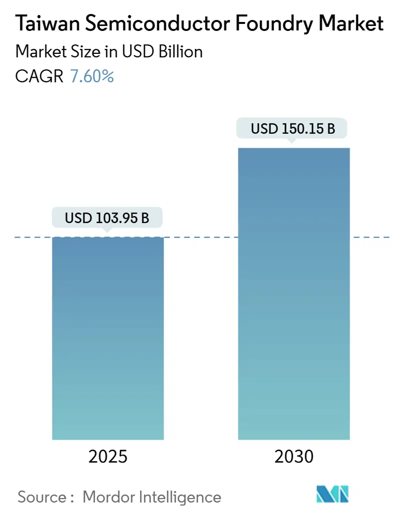
| Market Size (2025) | USD 103.95 Billion |
| Market Size (2030) | USD 150.15 Billion |
| Growth Rate (2025 - 2030) | 7.60% CAGR |
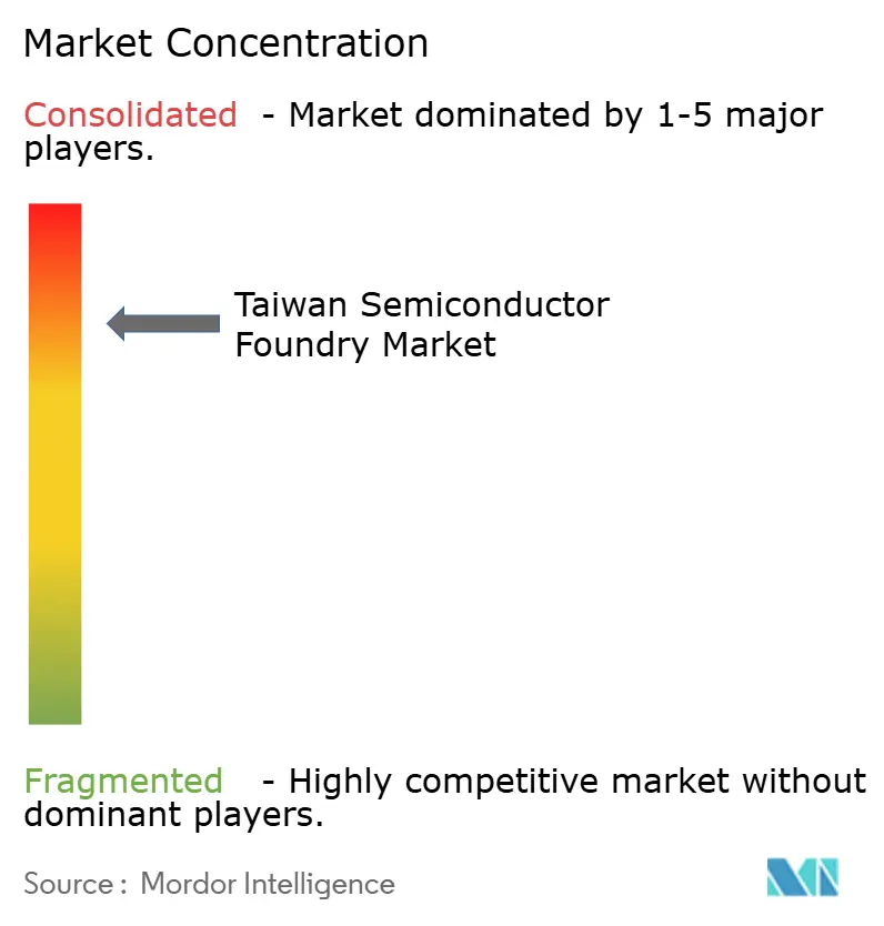
| Market Concentration | High |
Major Players
*Disclaimer: Major Players sorted in no particular order Image © Mordor Intelligence. Reuse requires attribution under CC BY 4.0. |
|
Taiwan Semiconductor Foundry Market Analysis by Mordor Intelligence
The Taiwan semiconductor foundry market size stands at USD 103.95 billion in 2025 and is projected to reach USD 150.15 billion by 2030, translating into a 7.6% CAGR across the forecast window. Demand for artificial-intelligence accelerators and high-performance-computing devices is driving the bulk of wafer starts, reinforced by TSMC’s 74% revenue contribution from 7 nm and below processes in the second quarter of 2025. Contract manufacturers benefit from robust pricing power at advanced nodes, sustained by strict supply–demand balance, rising die sizes, and accelerated design-win cycles among fabless chip firms. Parallel investment in 300 mm capacity, power-efficient back-side power delivery, and chiplet-ready advanced packaging elevates gross-margin resilience even as tool lead-times lengthen. Policy support through Taiwan’s Chips Act and continued science-park expansion provide predictable fiscal incentives that cushion capital-intensive scaling while helping the Taiwan semiconductor foundry market navigate geopolitical uncertainty.
Key Report Takeaways
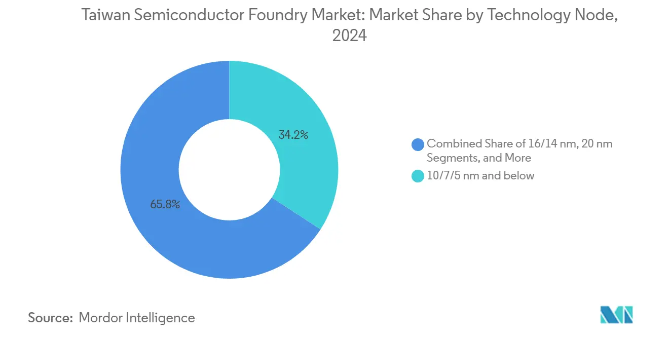
- By technology node, the 10/7/5 nm-and-below segment captured 34.2% of the Taiwan semiconductor foundry market share in 2024; 10/7/5 nm-and-below is forecast to expand at a 10.2% CAGR through 2030.
- By wafer size, 300 mm substrates accounted for 74.4% of the Taiwan semiconductor foundry market size in 2024 and are advancing at a 9.5% CAGR through 2030.
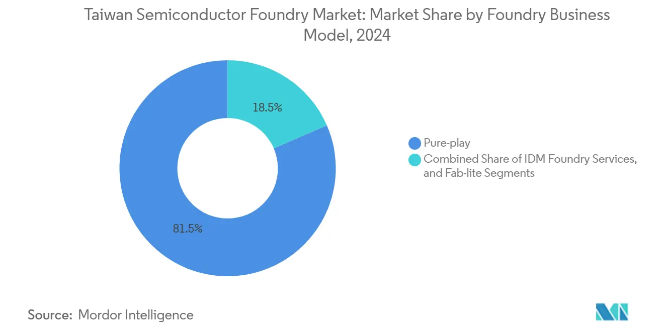
- By business model, pure-play operators held 81.5% revenue share of the Taiwan semiconductor foundry market in 2024 while growing at an 8.4% CAGR to 2030.
- By application, consumer electronics and communication represented 40.2% of the 2024 value; high-performance computing is projected to record the highest CAGR at 11.1% to 2030.
Worldwide, activity is shaped by contributions from multiple countries and regions, with Taiwan representing one among them. The global report on semiconductor foundry market by Mordor Intelligence reflects how these countries and regional layers combine into a single system.
Taiwan Semiconductor Foundry Market Trends and Insights
Drivers Impact Analysis*
| Driver | (~) % Impact on CAGR Forecast | Geographic Relevance | Impact Timeline |
|---|---|---|---|
| Explosive demand for advanced nodes (≤7 nm) for AI/HPC | +2.8% | Global, concentrated in Taiwan, and expanding to the US | Medium term (2-4 years) |
| Electrification of automotive platforms | +1.2% | Global, with strong growth in Asia-Pacific and Europe | Long term (≥ 4 years) |
| Government incentives and science-park expansion | +0.9% | Taiwan domestic, with spillover to international partnerships | Short term (≤ 2 years) |
| 5G/6G and IoT volume at mature nodes | +1.1% | Global, with early deployment in Asia-Pacific and North America | Medium term (2-4 years) |
| Back-side power and advanced packaging leadership | +0.7% | Taiwan-centric with technology transfer to overseas fabs | Medium term (2-4 years) |
| Chiplet ecosystem acceleration | +0.6% | Global, led by Taiwan foundries and US design companies | Long term (≥ 4 years) |
| Source: Mordor Intelligence | |||
Explosive Demand for Advanced Nodes Drives AI Revolution
Soaring inference workloads in generative-AI data centers transformed order books at 3 nm and 5 nm, making advanced nodes the primary value lever for the Taiwan semiconductor foundry market. TSMC’s shift to 2 nm mass production in late 2025 delivers 10–15% speed gains and 25–30% power reduction relative to 3 nm, locking in next-generation silicon for NVIDIA, AMD, and hyperscale cloud builders.[1]Taiwan Semiconductor Manufacturing Company, “TSMC Intends to Expand Its Investment in the United States to US $165 Billion,” pr.tsmc.com Nine additional 300 mm fabs and advanced-packaging plants now under construction will double monthly chip-on-wafer-on-substrate capacity by 2027. Concentrated AI demand raises average selling prices, funds step-function R&D, and accelerates the flywheel that keeps the Taiwan semiconductor foundry market two to three nodes ahead of competing regions.
Automotive Electrification Reshapes Semiconductor Requirements
Centralized computing in electric and software-defined vehicles pushes gigaflop budgets and dielectric reliability thresholds upward, opening new streams of non-mobile revenue. McKinsey forecasts global automotive semiconductor sales climbing toward USD 140 billion by 2032, a runway that positions Taiwan foundries to translate power-management and analog competency into predictable long-term wafer volumes. TSMC has already lifted automotive-qualified capacity by 50% since 2021 and advocates pre-booking buffer inventory to prevent shortage recurrence. Collaboration with Tier-1 suppliers on silicon carbide MOSFET drivers and zonal-architecture system-on-chips deepens design-service stickiness and enriches die mix, reinforcing the Taiwan semiconductor foundry market as the de facto back-end for EV compute subsystems.
Government Incentives Strengthen Taiwan’s Semiconductor Leadership
The 2024 Chips Act grants 25% tax credits on qualified R&D and a 5% allowance on new tool purchases, effectively lowering after-tax equipment costs in a capital cycle dominated by EUV scanners priced above USD 200 million a unit. Concurrent plans for a 1 nm pilot line inside a Silicon-Valley-style tech hub illustrate government willingness to allocate land and utilities in lockstep with corporate investment. An additional 2,000 hectares of science-park real estate under evaluation ensure long-term fab clustering, keeping the Taiwan semiconductor foundry market anchored on the island even as multinationals diversify. Fiscal tailwinds mitigate geopolitical risk premiums and sustain a built-in advantage over regions where incentives remain time-limited or procedurally complex.
5G / 6G Infrastructure Deployment Sustains Mature-Node Demand
Massive multi-input, multi-output radio units and edge-computing gateways rely on 22 nm to 40 nm technologies that combine RF, analog, and digital logic. Orders from telecom-equipment vendors extend production life cycles of depreciated fabs, supporting balanced utilization across node tiers. EdgeQ, a 5G baseband start-up, selected TSMC for its single-chip small-cell SoCs to capture private-network rollouts.[2]Cheng Ting-Fang, “Chip startup EdgeQ bets big on 5G private network boom,” Nikkei Asia, asia.nikkei.com UMC’s USD 5 billion Singapore plant, dedicated to 22 nm and 28 nm, anchors regional supply for mid-band transceivers and IoT sensors. Continued operator investment in densified 5G and pre-standard 6G testbeds maintains recurring revenue that buffers cyclicality in consumer electronics, adding an incremental lift to overall CAGR for the Taiwan semiconductor foundry market.
Restraints Impact Analysis*
| Restraint | (~) % Impact on CAGR Forecast | Geographic Relevance | Impact Timeline |
|---|---|---|---|
| Geopolitical trade/policy risk | -1.8% | Global, with concentrated impact on the Taiwan-China-US triangle | Short term (≤ 2 years) |
| Cap-ex intensity and tool lead-times | -1.1% | Global, affecting all major foundry regions | Medium term (2-4 years) |
| Water-supply vulnerability in southern fabs | -0.7% | Taiwan's domestic, particularly the southern regions | Long term (≥ 4 years) |
| Engineering-talent shortfall | -0.9% | Taiwan's domestic market with spillover to international expansion | Medium term (2-4 years) |
| Source: Mordor Intelligence | |||
Geopolitical Trade Tensions Create Strategic Vulnerabilities
Trade-policy gyrations inject tariff uncertainty that complicates long-term allocation of advanced-node production between Taiwan and overseas subsidiaries. A proposed 32% duty on Taiwan-origin graphics-processing devices could undermine the cost parity of U.S. AI start-ups, despite Taiwan accounting for 46% of 2024 GPU imports to America. TSMC’s USD 165 billion United States build-out partially de-risks access but imposes operating-margin compression because of higher labor costs and fragmented supply chains. Cross-strait tensions amplify inventory-buffer strategies at global OEMs, creating non-productive working-capital swings and reducing near-term visibility for the Taiwan semiconductor foundry market.
Capital Expenditure Intensity Strains Financial Resources
Record 300 mm equipment outlays of USD 137 billion expected in 2027 magnify cash-flow demands, and Taiwan alone is slated to absorb USD 28 billion of that total.[3]“300 mm Fab Equipment Spending Forecast to Reach Record $137 Billion,” SEMI, semi.org TSMC’s 2025 cap-ex guidance of up to USD 42 billion equals almost 40% of projected sales, highlighting the perpetual funding required to keep performance on the Moore-curve law trajectory. Tool lead-times above 18 months for EUV scanners delay ramp schedules, obliging staggered start-ups that can push revenue recognition into later quarters. Any abrupt macro shock that limits free-cash generation could delay node introductions, shaving growth off the Taiwan semiconductor foundry market CAGR baseline.
*Our forecasts treat driver/restraint impacts as directional, not additive. The impact forecasts reflect baseline growth, mix effects, and variable interactions.
Segment Analysis
By Technology Node: Advanced Processes Dominate Value Creation
The sub-10 nm tier accounted for 34.2% of 2024 revenue, the highest within the Taiwan semiconductor foundry market, and is pacing an estimated 10.2% CAGR through 2030. The segment benefited from the August 2025 start of 2 nm risk production that promises superior transistor density and 25–30% lower power draw versus 3 nm contemporaries. While 16/14 nm lines serve mixed-signal infotainment and industrial automation, premium margins cluster at bleeding-edge nodes where design tape-outs often exceed USD 500 million. Samsung’s 13% worldwide share underscores competitive fragmentation as Intel and UMC explore collaborative 12 nm developments aimed at legacy advanced nodes. Sustained pricing discipline and volume skews toward AI accelerators ensure that the Taiwan semiconductor foundry market size for this node class maintains double-digit growth despite the capital burden.
Investment in older geometries remains purposeful. 28 nm retains a strategic role in OLED driver ICs and 40 nm in secure MCU families shipped into payment terminals, guaranteeing cyclical utilization as smartphone refresh rates plateau. Taiwan manufacturers exploit depreciated toolsets to undercut rivals on unit cost without sacrificing automotive AEC-Q100 qualifications, extending the economic life of 45 nm and 65 nm flows. The resulting bimodal portfolio lets foundries harvest cash from mature nodes that finance front-end innovation, reinforcing the flywheel that propels the Taiwan semiconductor foundry market.


By Wafer Size: 300 mm Substrates Enable Scale Economics
The 300 mm category captured 74.4% of 2024 billings and is expanding at a 9.5% CAGR through 2030, illustrating how wafer surface economics scale transistor output per process step. Every incremental 25 mm of diameter yields about 25% more dies when accounting for scribe lanes and edge losses, lowering per-die depreciation and utility loads. All nine fabs announced by TSMC for 2025 deploy 300 mm configurations, targeting a combined monthly throughput exceeding 600,000 wafers when fully equipped. The Taiwan semiconductor foundry market size advantage at 300 mm broadens as AI ASICs migrate to multi-reticle system-on-wafer designs that demand extensive exposure to real estate.
Conversely, 200 mm retains resonance for power discretes and analog ICs, where die shrink offers limited functional gain relative to package constraints. Specialty processes for GaN FETs and silicon carbide Schottky diodes inhabit 150 mm or smaller wafer sets, often inside repurposed facilities that operate at lower cost structures. Steady shipments to automotive traction inverters and industrial drives keep tool utilization above 80%, supporting bottom-line contribution. The calibrated coexistence of diameter tiers contributes to balanced asset leverage within the Taiwan semiconductor foundry market.
By Foundry Business Model: Pure-Play Model Proves Superior
Pure-play operators generated 81.5% of sector turnover in 2024 and are forecast to log an 8.4% CAGR to 2030, underscoring client preference for conflict-free manufacturing partners. TSMC’s roster of over 500 fabless customers ranges from consumer SoC champions to aerospace classified-grade ASIC contractors, spreading fixed-cost recovery across a wide revenue base. IDM foundry services, representing 18.5% of value, mostly cover captive demand as brand concerns discourage rivals from entrusting designs to vertically integrated competitors. Fab-lite participants shrink as chipmakers embrace either a fully asset-light stance or double down on internal fabs, limiting mid-spectrum appeal.
Strategic commitments to open-standard design enablement further amplify the pull of pure-play capacity. Co-development of backside power integration and co-packaged optics with leading EDA suppliers cements a differentiated technology roadmap unavailable to IDM rivals. Simultaneously, Taiwan operators apply Foundry 2.0 corporate governance to reassure regulators about antitrust risks, sustaining long-run access to critical lithography gear. These dynamics reinforce the revenue durability of the pure-play cohort inside the Taiwan semiconductor foundry market.
By Application: HPC Emerges as Growth Engine
Consumer electronics and communication devices delivered 40.2% of 2024 revenue, reflecting legacy smartphone and notebook volumes. Yet high-performance computing wafers, though smaller in absolute shipments, are trending at an 11.1% CAGR through 2030 and draw premium pricing that inflates blended ASP. Google’s identification of Taiwan as the anchor for its AI silicon supply stack indicates how cloud platforms entrust mission-critical workloads to the region. CoWoS capacity, forecast to eclipse 10% of TSMC sales in 2025, underscores packaging as a competitive choke point that locks AI accelerator orders to Taiwan fabs.
Automotive orders climb steadily as BEV adoption pushes semiconductor content per vehicle toward USD 1,600, spanning power-management ICs, image processors, and domain controllers. Meanwhile, industrial and IoT customers sustain legacy node fabs with predictable run-rate programs, ensuring diversified loading. The application mix thus distributes cyclical risk while leaving the Taiwan semiconductor foundry market poised for structural uplift as AI-centric capital budgets continue to scale.
Geography Analysis
Taiwan generated 68.8% of worldwide outsourced wafer revenue in 2024 and produced 83% of the planet’s AI chips, confirming its unmatched ecosystem density. The Southern Taiwan Science Park exceeded NT$2.21 trillion (USD 68.23 billion) turnover in 2024 and is targeting NT$3 trillion in 2025, primarily on the back of 3 nm ramp volumes. Local infrastructure advantages—proximity to substrates, chemicals, and advanced-packaging lines—compress cycle time from design tape-out to risk production, reinforcing sovereign advantages for the Taiwan semiconductor foundry market.
Asia-Pacific partners amplify resilience. UMC’s Singapore expansion adds 30,000 wafers a month of 22 nm and 28 nm output, diversifying geopolitical exposure while leveraging strong local photonics talent. Japan’s Kumamoto cluster, co-funded by TSMC and government subsidies, provides regional risk hedging but grapples with land and water constraints that limit the speed of scale. India’s first fab at Dholera, backed by Tata and PSMC, positions South Asia as a future hub for mature-node demand, though ecosystem build-out remains in its infancy.[4]Tata Group, “Tata Group to Build the Nation’s First Fab in Dholera,” tata.com
North America and Europe pivot toward security-of-supply imperatives. TSMC’s Phoenix campus highlights how incentive-driven foreign direct investment can localize bleeding-edge logic, but cost structures remain higher and supply-chain orchestration more complex than in Taiwan. The Dresden joint venture with Bosch, Infineon, and NXP replicates this model in Europe, advancing strategic autonomy for automotive chips. In both cases, knowledge diffusion accrues from Taiwanese engineers deployed overseas, underpinning global relevance for the Taiwan semiconductor foundry market while preserving research cores on the island.
Mordor Intelligence provides coverage of the semiconductor foundry market across other key regional markets. Detailed country-level analysis extends to Singapore, South Korea, Japan, Germany, China, United States, Malaysia, and Israel incorporating local coverage and market participation, as required.
Competitive Landscape
TSMC retained a major share of worldwide foundry revenue in 2024, an outsized share that magnifies economies of learning and tool-procurement leverage. Quarterly revenue touched NT$323.2 billion (USD 10.83 billion) in July 2025, a 26% year-on-year surge propelled by generative-AI accelerator wafers. United Microelectronics Corporation ranks second yet concentrates on specialty RF and embedded non-volatile memory flows, a strategy that minimizes node-for-node rivalry and stabilizes base-load for the Taiwan semiconductor foundry market. VIS and PSMC round out the domestic roster, focusing on power devices and display drivers, respectively.
Strategic differentiation increasingly hinges on packaging leadership. TSMC’s chip-on-wafer-on-substrate throughput is slated to double by 2027 following NT$1.5 trillion expansion in Kaohsiung. ASE Technology’s NT$6.5 billion acquisition of a Kaohsiung plant accelerates outsourced assembly capacity, aligning substrate supply with front-end die volumes. Market participants also race to secure reclaimed wafer and chemicals supply, evidenced by Phoenix Silicon’s plan to double cap-ex to NT$7.9 billion for reclaimed wafer output.
White-space competition emerges in automotive microcontrollers, biomedical sensor arrays, and gallium-nitride power devices, where Chinese peers face export-control friction. Taiwanese firms partner with European and U.S. system integrators to fast-track qualification, a corridor that can augment long-run revenue diversity. The result is a bifurcated ecosystem: TSMC dominates advanced logic, while mid-tier Taiwanese fabs specialize in capturing sticky verticals, collectively anchoring the Taiwan semiconductor foundry market.
Taiwan Semiconductor Foundry Industry Leaders
-
United Microelectronics Corporation (UMC)
-
Taiwan Semiconductor Manufacturing Company Limited (TSMC)
-
Vanguard International Semiconductor Corporation (VIS)
-
Powerchip Semiconductor Manufacturing Corp. (PSMC)
-
WIN Semiconductors Corp.
- *Disclaimer: Major Players sorted in no particular order

Recent Industry Developments
- August 2025: ASE Technology Holding acquired a Kaohsiung manufacturing plant from Win Semiconductors for NT$6.5 billion (USD 216.48 million) to expand advanced IC assembly.
- August 2025: King Yuan Electronics raised 2025 capital expenditure by 37% to NT$37 billion (USD 1.24 billion) and injected S$100 million (USD 77.8 million) into its Singapore arm for capacity expansion.
- July 2025: TSMC began building four Central Taiwan Science Park fabs labeled Fab 25, targeting 2 nm production by late 2028 with 50,000-wafer monthly output.
- July 2025: Hon Hai Precision and Teco Electric formed a partnership to pursue AI data-center opportunities, including a 10% equity swap.


Taiwan Semiconductor Foundry Market Report Scope
| 10/7/5 nm and below |
| 16/14 nm |
| 20 nm |
| 28 nm |
| 45/40 nm |
| 65 nm and above |
| 300 mm |
| 200 mm |
| <150 mm |
| Pure-play |
| IDM Foundry Services |
| Fab-lite |
| Consumer Electronics and Communication |
| Automotive |
| Industrial and IoT |
| High-Performance Computing (HPC) |
| Other Applications |
| By Technology Node | 10/7/5 nm and below |
| 16/14 nm | |
| 20 nm | |
| 28 nm | |
| 45/40 nm | |
| 65 nm and above | |
| By Wafer Size | 300 mm |
| 200 mm | |
| <150 mm | |
| By Foundry Business Model | Pure-play |
| IDM Foundry Services | |
| Fab-lite | |
| By Application | Consumer Electronics and Communication |
| Automotive | |
| Industrial and IoT | |
| High-Performance Computing (HPC) | |
| Other Applications |


Key Questions Answered in the Report
How large is the Taiwan semiconductor foundry market today?
The Taiwan semiconductor foundry market size is USD 103.95 billion in 2025 and is forecast to hit USD 150.15 billion by 2030.
What CAGR is expected for Taiwan’s contract-manufacturing wafer sector?
Aggregate value is projected to grow at a 7.6% CAGR between 2025 and 2030.
Which technology node leads revenue contribution in Taiwan fabs?
The 10/7/5 nm-and-below class delivered 34.2% of 2024 revenue and is expanding fastest at a 10.2% CAGR.
Why are 300 mm wafers strategically important?
They hold a 74.4% share of output and reduce per-die cost, making them central to AI and HPC chip economics.
How exposed is Taiwan’s foundry supply chain to geopolitical risk?
Geopolitical tariff proposals and cross-strait tensions pose near-term headwinds that could reduce forecast CAGR by up to 1.8%.
What role does advanced packaging play in Taiwan’s competitive edge?
Technologies such as chip-on-wafer-on-substrate are capacity-constrained yet critical for AI accelerators, reinforcing Taiwan’s leadership.
Page last updated on:


