Singapore Semiconductor Foundry Market Size and Share
Market Overview
| Study Period | 2019 - 2030 |
|---|---|
| Forecast Data Period | 2025 - 2030 |
| Historical Data Period | 2019 - 2023 |
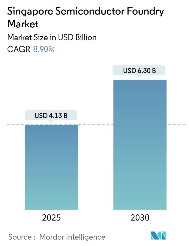
| Market Size (2025) | USD 4.13 Billion |
| Market Size (2030) | USD 6.30 Billion |
| Growth Rate (2025 - 2030) | 8.90% CAGR |
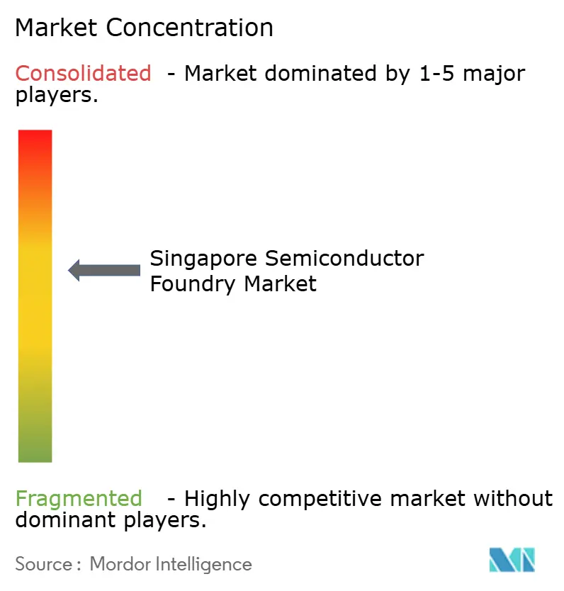
| Market Concentration | Medium |
Major Players
*Disclaimer: Major Players sorted in no particular order Image © Mordor Intelligence. Reuse requires attribution under CC BY 4.0. |
|
Singapore Semiconductor Foundry Market Analysis by Mordor Intelligence
The Singapore semiconductor foundry market size** stands at USD 4.13 billion in 2025 and is forecast to reach USD 6.3 billion by 2030, translating into an 8.9% CAGR over the period. Strong government incentives, a geopolitically neutral stance, and deep-rooted expertise in mature-node processes position the nation as a preferred alternative to traditional fabrication hubs.[1]Economic Development Board, “What Makes Singapore a Prime Location for Semiconductor Companies Driving Innovation?,” edb.gov.sg Capacity expansions at GlobalFoundries, UMC, and the VisionPower-NXP–NXP joint venture indicate confidence that Singapore can deliver both quality and scale despite higher operating costs. Demand from regional electric-vehicle and high-performance-computing customers bolsters utilization rates, while the National Research Foundation’s advanced-node prototyping program widens the domestic innovation pipeline. At the same time, escalating energy prices and a tightening labor market temper growth prospects, nudging manufacturers toward automation and sustainability investments that protect margins over the long term.
Key Report Takeaways
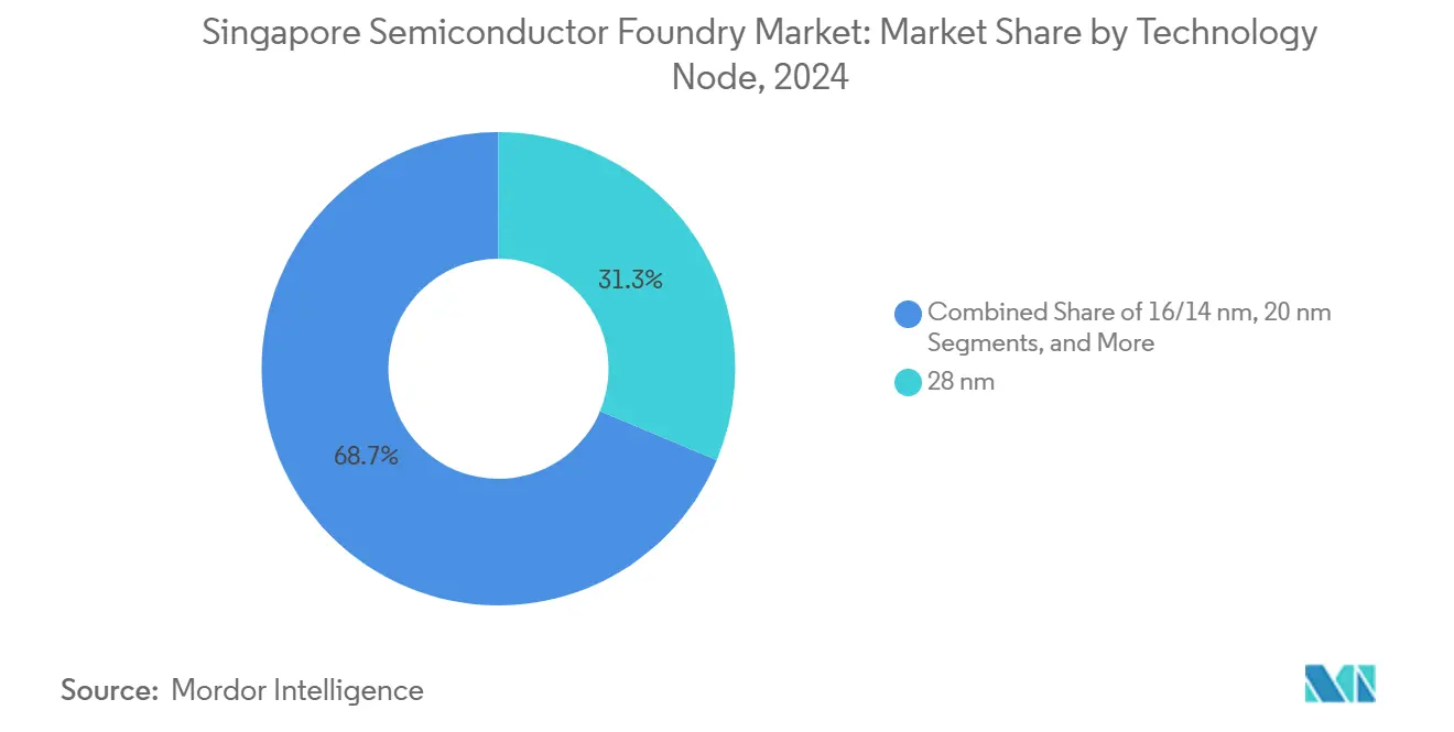
- By technology node, 28 nm processes held 31.3% of the **Singapore semiconductor foundry market share** in 2024; 10 / 7 / 5 nm and below is projected to grow at 14.8% CAGR through 2030.
- By wafer size, 300 mm accounted for 66.6% share of the **Singapore semiconductor foundry market size** in 2024 and is expanding at 12.4% CAGR to 2030.
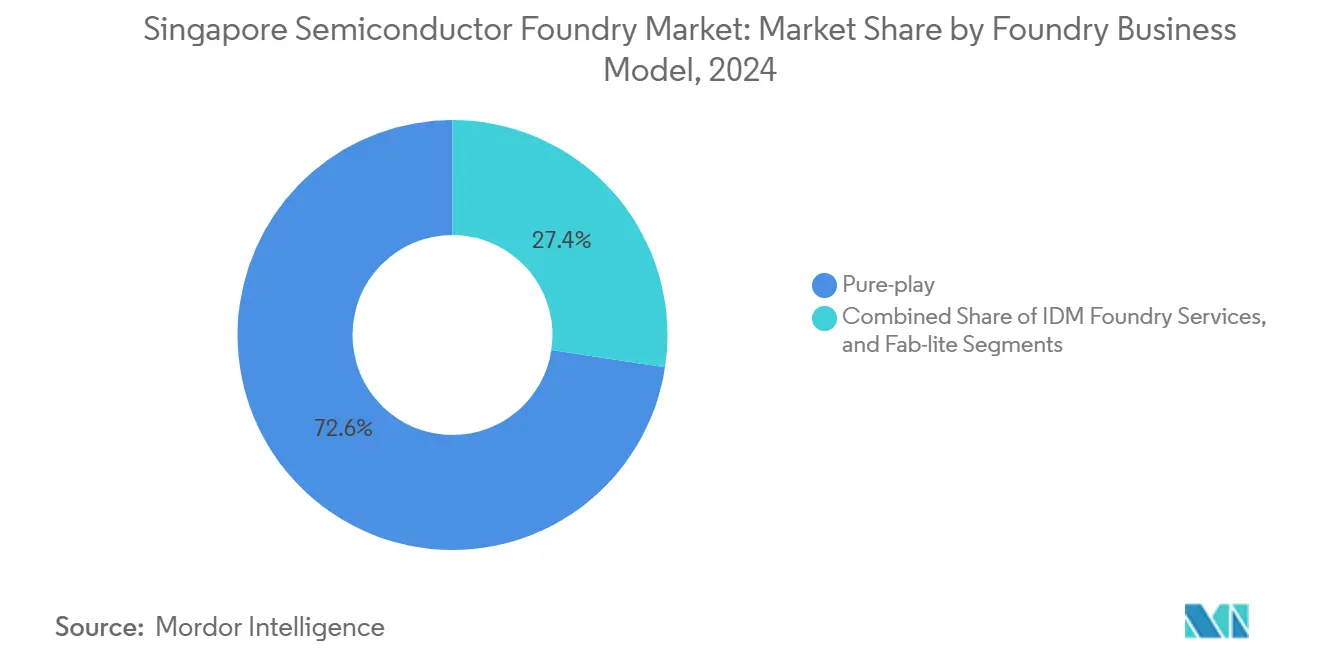
- By business model, pure-play services captured 72.6% revenue share in 2024, while IDM foundry services posted the highest projected CAGR at 13.2% through 2030.
- By application, consumer electronics led with 38.3% revenue share in 2024; high-performance computing is advancing at 15.1% CAGR through 2030.
Global valuation is built by aggregating outputs from multiple countries and regions, with Singapore being one of the contributors. Our global semiconductor foundry market size represents that cumulative total.
Singapore Semiconductor Foundry Market Trends and Insights
Drivers Impact Analysis*
| Driver | (~) % Impact on CAGR Forecast | Geographic Relevance | Impact Timeline |
|---|---|---|---|
| Government incentives under Singapore's Semiconductor Industry Transformation Map 2.0 | +1.2% | National, with spillover to regional supply chains | Medium term (2-4 years) |
| Expanding 300mm capacity at GlobalFoundries' Tampines Megafab | +0.8% | National, supporting Asia-Pacific automotive supply chains | Short term (≤ 2 years) |
| Surging automotive-grade chip demand from regional EV makers | +1.5% | Asia-Pacific core, with concentration in Singapore and Malaysia | Long term (≥ 4 years) |
| National Research Foundation's sub-10nm multi-project wafer program | +0.7% | National, with technology transfer to regional partners | Long term (≥ 4 years) |
| Growth of advanced 3D heterogeneous packaging clusters | +0.9% | National, with a global customer base | Medium term (2-4 years) |
| Local data-centre energy caps driving HPC node innovation | +0.6% | National, with implications for regional data center infrastructure | Medium term (2-4 years) |
| Source: Mordor Intelligence | |||
Government incentives under Singapore's Semiconductor Industry Transformation Map 2.0
More than SGD 500 million is earmarked to establish a shared national fabrication facility by 2027 that supports advanced packaging, heterogeneous integration, and small-batch prototyping. The funding helps startups and SMEs gain access to industry-grade tools, narrowing the cost and capability gap with larger peers. Translational research is prioritized, allowing design houses to commercialize specialty devices faster. Early-stage projects already report a 3:1 ratio of private to public co-investment, hinting at strong multiplier effects. By fostering closer ties between academia and industry, the scheme cultivates skilled talent and intellectual property that anchor future production runs in Singapore.
Expanding 300 mm capacity at GlobalFoundries' Tampines Megafab
The Tampines site’s phased expansion brings an additional 28 nm automotive-qualified lines online in 2026, boosting national 300 mm output for power-management and analog chips.[2]GlobalFoundries Inc., “GlobalFoundries Reports First Quarter 2024 Financial Results,” gf.com Automotive OEMs value the facility’s AEC-Q100 certifications, enabling multi-year supply agreements. Mature-node specialization delivers attractive margins because fewer competitors can match stringent reliability thresholds. Capacity is aligned with customer call-offs from European and Asian automakers that are scaling EV production. Automation upgrades trim cycle times, further differentiating the fab from cost-driven rivals.
Surging automotive-grade chip demand from regional EV makers
High-end EVs use more than 3,000 semiconductor components, tripling the content of conventional vehicles. Singapore’s fabs concentrate on power devices, battery-management ICs, and sensor hubs, all of which are pivotal for autonomous and electrified drivetrains. Southeast Asian and Chinese carmakers are dual-sourcing away from Taiwan, elevating Singapore’s order book. Long qualification cycles and functional-safety requirements deter new entrants and lock in dependable revenue streams. Complementary back-end services in neighboring Malaysia create a cohesive regional EV chip cluster that appeals to global tier-1 suppliers.
National Research Foundation's sub-10 nm multi-project wafer program
The program lets local design houses tape out test chips on leading-edge nodes without bearing full foundry costs.[3]National Research Foundation Singapore, “Medium-Sized Centre,” nrf.gov.sg Access to advanced lithography accelerates AI, 5G, and quantum device R&D while sharpening workforce skills in extreme-ultraviolet process flows. Participation agreements include knowledge-transfer clauses that gradually embed best practices into Singaporean fabs. Spin-off IP can be licensed to global chip leaders, opening royalty revenue channels. Over time, the initiative seeds a pipeline of complex devices that will migrate to mass production when commercial volumes justify new capex.
Restraints Impact Analysis*
| Restraint | (~) % Impact on CAGR Forecast | Geographic Relevance | Impact Timeline |
|---|---|---|---|
| High energy and water intensity versus Singapore's Green Plan 2030 | -0.8% | National, with implications for regional manufacturing costs | Long term (≥ 4 years) |
| Shortage of experienced semiconductor engineers | -1.1% | National, with regional talent competition effects | Short term (≤ 2 years) |
| Scarcity of industrial land for new fabs post-2030 | -0.6% | National, affecting long-term capacity expansion | Long term (≥ 4 years) |
| Export-control risks around EUV tool deliveries | -0.4% | Global, with specific implications for Singapore's advanced-node ambitions | Medium term (2-4 years) |
| Source: Mordor Intelligence | |||
High energy and water intensity versus Singapore's Green Plan 2030
Semiconductor plants and data centers already strain the national grid, challenging net-zero targets for 2050. New fabs must adopt energy-recovery systems, on-site solar, and advanced water-reclaim modules, inflating upfront costs and lengthening ROI periods. While incentives for green technologies partially offset these expenses, ongoing carbon-pricing mechanisms threaten operating margins. Companies pursuing Scope 3 emissions reductions prefer suppliers with verifiable sustainability credentials, pressuring laggards to accelerate eco-upgrades. Balancing capacity growth with environmental stewardship remains a delicate policy trade-off.
Shortage of experienced semiconductor engineers
Vacancy rates for process-integration and equipment-maintenance roles climbed into double digits in 2024, prompting the Ministry of Manpower to add multiple semiconductor job titles to its Shortage Occupation List.[4]Economic Development Board, “How Is Singapore Developing Semiconductor Talent to Meet Industry Needs?,” edb.gov.sg Engineering salaries rose at least 15% year over year as firms competed with Malaysian and Taiwanese employers that dangled relocation bonuses. Polytechnics are boosting intake for microelectronics courses, but new cohorts will not graduate before 2027. In the interim, manufacturers rely on accelerated reskilling programs and foreign-talent quotas to staff expansions. Elevated labor costs narrow Singapore’s pricing latitude, though automation mitigates some pressure.
*Our forecasts treat driver/restraint impacts as directional, not additive. The impact forecasts reflect baseline growth, mix effects, and variable interactions.
Segment Analysis
By Technology Node: Mature Nodes Drive Automotive Revolution
The 28 nm node accounted for 31.3% of 2024 revenue, underscoring customer preference for reliable and cost-effective platforms that meet functional-safety standards. The **Singapore semiconductor foundry market** leverages this sweet spot to anchor long-term contracts with EV and industrial clients. Demand for 16 / 14 nm and 20 nm processes is growing as autonomous driving and smart-factory installations need higher performance without incurring leading-edge costs. Meanwhile, sub-10 nm prototypes emerge from NRF’s wafer program, positioning local design houses for future high-performance computing opportunities. Advanced-node output is limited today, yet its 14.8% CAGR signals an eventual pivot toward AI accelerators and data-center SoCs.
Rapid deployment of EUV tooling is contingent on export-control clearances, placing a ceiling on immediate capacity. Nonetheless, Singapore’s process-engineer talent pool in mature nodes remains a differentiator because automotive and industrial buyers place more weight on yield and reliability than on sheer transistor density. The balanced node mix shields fabs from cyclicality in consumer electronics while providing an upgrade path should advanced-node economics improve. Ongoing investments by UMC and VisionPower at the 22 / 28 nm range reinforce the nation’s specialization in volume production for powertrain and safety systems, sustaining pricing power in a segment less vulnerable to aggressive Chinese competition.


By Wafer Size: 300 mm Infrastructure Dominance
The Singapore semiconductor foundry market size for 300 mm wafers constituted 66.6% of total output in 2024 and is projected to grow at a 12.4% CAGR, propelled by economies of scale and high automotive chip volumes. Larger wafers lower per-die costs, giving local fabs an edge when bidding for multi-year EV contracts. Automation investments boost throughput and yield, allowing plants to balance premium quality with competitive pricing. JTC’s land-reservation strategy earmarks more space for 300 mm parks, ensuring expansion headroom through the decade.
Conversely, 200 mm lines serve RF, analog, and MEMS applications where redesign costs preclude migration. Although share falls gradually, these lines remain profitable due to niche demand and depreciated equipment. Wafers below 150 mm fill legacy or specialty needs, but growth is negligible. Singapore’s focus on 300 mm capacity aligns with global trends toward chiplet and heterogeneously integrated devices that benefit from advanced packaging performed on larger substrates. The resulting scale consolidates the country’s role as a regional powerhouse for high-volume automotive and industrial semiconductors.
By Foundry Business Model: Pure-Play Specialization Strategy
Pure-play operators captured 72.6% of 2024 revenue, validating Singapore’s orientation toward contract manufacturing over integrated device production. The model allows GlobalFoundries, UMC, and VisionPower to service multiple fabless and IDM clients without channel conflicts. High equipment utilization improves cost recovery, supporting reinvestment in specialty processes and automotive qualifications. IDMs that require custom chemistries or security assurances increasingly outsource overflow production, adding incremental volumes to pure-play lines.
Fab-lite activity remains marginal because the capital intensity of new fabs discourages partial outsourcing strategies. Instead, firms either commit fully to outsourcing or invest in dedicated captive capacity. The **Singapore semiconductor foundry market** benefits from pure-play flexibility, which lets fabs quickly allocate capacity to the highest-margin segments during up-cycles while maintaining long-term agreements for stable utilization. Upcoming 22 / 28 nm expansions by UMC and VisionPower further entrench the pure-play model, cementing Singapore’s reputation as a trusted third-party manufacturing hub for automotive-grade chips.
By Application: Consumer Electronics Leadership with HPC Acceleration
Consumer electronics and communication devices represented 38.3% of 2024 wafer starts, reflecting deep ties to Asian smartphone and IoT assemblers. Even so, high-performance computing logged the fastest expansion at 15.1% CAGR, buoyed by AI-driven server demand. The trend opens premium revenue streams as Singapore fabs qualify for high-density SRAM and interposer-based GPU production. Automotive applications continue their sharp ascent, catalyzed by regional EV initiatives that mandate larger silicon content per vehicle.
Industrial and IoT segments sustain steady mid-single-digit growth, supported by Singapore’s smart-nation initiatives and ASEAN factory automation projects. Other categories—medical, aerospace, and telecom infrastructure—round out demand without dominating capacity allocations. The evolving mix enhances resilience by diversifying away from cyclical consumer-device orders. It also complements government priorities to capture higher-value micro-electronics, positioning the **Singapore semiconductor foundry market** for sustained profitability even amid global supply-chain realignments.
Geography Analysis
Singapore’s harbor location and world-class logistics network enable same-day shipment of processed wafers to Malaysian OSAT partners, slashing cycle times for automotive customers that require tight delivery windows. Proximity to Japanese chemical suppliers and South Korean equipment vendors streamlines inbound supply, thereby reducing buffer inventory needs and working capital. These structural advantages underpin the **Singapore semiconductor foundry market** as regional demand for EV and AI chips accelerates.
Complementarity rather than rivalry characterizes the relationship with neighboring Malaysia, whose assembly and test houses absorb Singapore’s front-end output. Joint customer roadshows showcase an integrated ASEAN value chain that offers risk diversification from single-site dependence in Taiwan or mainland China. Meanwhile, Vietnam and Indonesia court entry-level fabs with lower labor costs, but limited infrastructure and longer customs clearance keep them from eroding Singapore’s core mature-node niche.
Still, intense competition from mainland China’s subsidized fabs exerts pricing pressure that Singapore counters with zero-defect quality records and ISO 26262 compliance. Government-backed R&D hubs ensure that local fabs stay technologically relevant even as they focus on mature nodes. As the Asia-Pacific semiconductor market edges toward the USD 30 billion mark by 2030, Singapore’s steady 8.9% CAGR signals that its strategy of quality-led specialization remains viable despite rising regional challengers.
Coverage of the semiconductor foundry market by Mordor Intelligence spans a wide geographic footprint, with detailed country-level intelligence for China, Malaysia, Taiwan, Japan, South Korea, Germany, United States, and Israel, each shaped by local operating conditions.
Competitive Landscape
The national market hosts a handful of dominant players, with GlobalFoundries, UMC, and the VisionPower-NXP venture collectively holding a significant share of installed capacity. Their leadership rests on specialized automotive qualifications, robust customer audits, and long-standing ties with tier-1 system suppliers. New entrants face steep capex and rigorous reliability certifications that extend qualification cycles beyond two years, naturally limiting overcrowding.
Strategic focus gravitates toward Industry 4.0 process control. Plants deploy IoT sensors, big data analytics, and closed-loop yield management to offset higher wage costs. For example, GlobalFoundries’ Tampines site adopted AI-driven metrology that reduced line-defect rates by double digits, securing repeat orders from European automakers. At UMC, predictive-maintenance algorithms trimmed downtime, allowing the fab to ramp 28 nm volumes ahead of contract milestones.
Collaboration with equipment giants adds another layer of differentiation. Applied Materials’ EPIC platform anchors a local ecosystem for advanced packaging R&D, giving Singapore fabs early access to next-generation tools. Micron’s forthcoming HBM packaging plant will intensify knowledge spillovers in high-bandwidth memory assembly, widening capability gaps versus lower-cost jurisdictions. Despite the moderate concentration, competitive intensity stays in check because each major player targets distinct application slices, minimizing head-to-head price wars.
Singapore Semiconductor Foundry Industry Leaders
-
GlobalFoundries Singapore Pte. Ltd.
-
United Microelectronics Corporation
-
Taiwan Semiconductor Manufacturing Company Ltd.
-
Samsung Foundry
-
Tower Semiconductor Ltd.
- *Disclaimer: Major Players sorted in no particular order

Recent Industry Developments
- March 2025: A national semiconductor R&D facility worth SGD 500 million was announced for Tampines, giving SMEs access to shared tools by 2027.
- January 2025: Micron Technology broke ground on a USD 7 billion high-bandwidth-memory packaging facility that will initially create 1,400 jobs and expand to 3,000 positions, strengthening Singapore’s role in AI-centric devices.
- December 2024: VisionPower Semiconductor Manufacturing Company began construction on a USD 7.8 billion 300 mm fab slated for 55,000 wafers per month by 2029, the largest single semiconductor investment in Singapore.
- November 2024: Applied Materials launched its EPIC collaboration model to accelerate the commercialization of advanced chip-packaging technologies in partnership with A*STAR.


Singapore Semiconductor Foundry Market Report Scope
| 10/7/5 nm and below |
| 16/14 nm |
| 20 nm |
| 28 nm |
| 45/40 nm |
| 65 nm and above |
| 300 mm |
| 200 mm |
| <150 mm |
| Pure-play |
| IDM Foundry Services |
| Fab-lite |
| Consumer Electronics and Communication |
| Automotive |
| Industrial and IoT |
| High-Performance Computing (HPC) |
| Other Applications |
| By Technology Node | 10/7/5 nm and below |
| 16/14 nm | |
| 20 nm | |
| 28 nm | |
| 45/40 nm | |
| 65 nm and above | |
| By Wafer Size | 300 mm |
| 200 mm | |
| <150 mm | |
| By Foundry Business Model | Pure-play |
| IDM Foundry Services | |
| Fab-lite | |
| By Application | Consumer Electronics and Communication |
| Automotive | |
| Industrial and IoT | |
| High-Performance Computing (HPC) | |
| Other Applications |


Key Questions Answered in the Report
How large is the Singapore semiconductor foundry market today?
It is valued at USD 4.13 billion in 2025 and is projected to reach USD 6.3 billion by 2030.
What CAGR is expected for Singapore’s foundry sector?
The market is forecast to expand at an 8.9% CAGR between 2025 and 2030.
Which technology node dominates national output?
Mature 28 nm processes led with 31.3% revenue share in 2024 due to strong automotive and industrial demand.
Why is 300 mm wafer capacity so important in Singapore?
The 300 mm segment represents 66.6% of output and grows at 12.4% CAGR because larger wafers cut per-die costs for high-volume automotive chips.
What challenges could slow foundry expansion?
Rising energy costs tied to Green Plan 2030 and a shortage of experienced semiconductor engineers weigh on near-term growth.
Which companies are investing the most in new fabs?
UMC, the VisionPower-NXP–NXP joint venture, and GlobalFoundries each have multi-billion-dollar projects that expand 22 / 28 nm capacity through 2029.
Page last updated on:


