Japan Semiconductor Foundry Market Size and Share
Market Overview
| Study Period | 2019 - 2030 |
|---|---|
| Forecast Data Period | 2025 - 2030 |
| Historical Data Period | 2019 - 2023 |
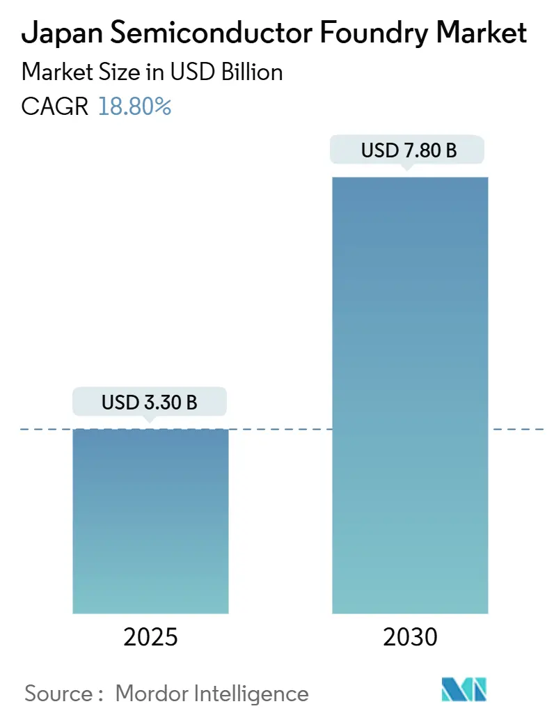
| Market Size (2025) | USD 3.30 Billion |
| Market Size (2030) | USD 7.80 Billion |
| Growth Rate (2025 - 2030) | 18.80% CAGR |
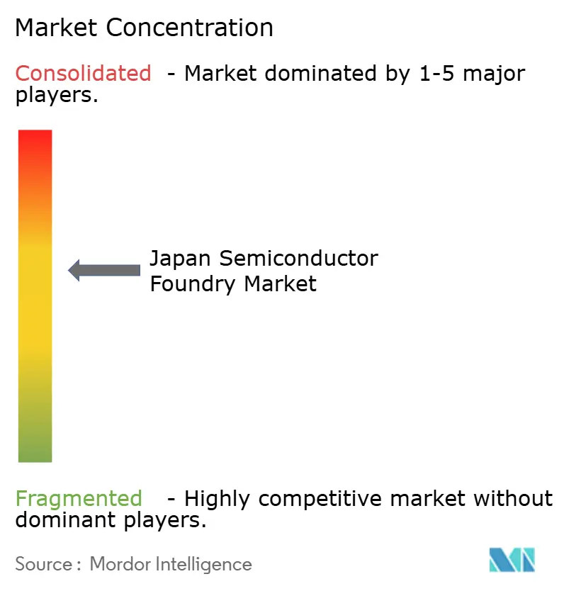
| Market Concentration | Medium |
Major Players
*Disclaimer: Major Players sorted in no particular order Image © Mordor Intelligence. Reuse requires attribution under CC BY 4.0. |
|
Japan Semiconductor Foundry Market Analysis by Mordor Intelligence
The Japan semiconductor foundry market size is USD 3.3 billion in 2025 and is predicted to expand at an 18.8% CAGR to USD 7.8 billion by 2030. A surge of public funding, private-sector alliances, and a decisive pivot to 2 nm-class production have reversed three decades of contraction, turning Japan into a preferred site for resilient, high-end capacity. Accelerated subsidy disbursements are shortening build-out cycles to <24 months, while automotive electrification and edge-AI adoption are front-loading near-term demand. Foreign operators gain guaranteed offtake volumes by co-locating with tier-one electronics and vehicle OEMs, and domestic groups leverage long-standing supplier relationships to secure early design-in wins. Intensifying competition raises talent, power, and land costs, but also compels new process and packaging innovations that position the country for sustained premium pricing.
Key Report Takeaways
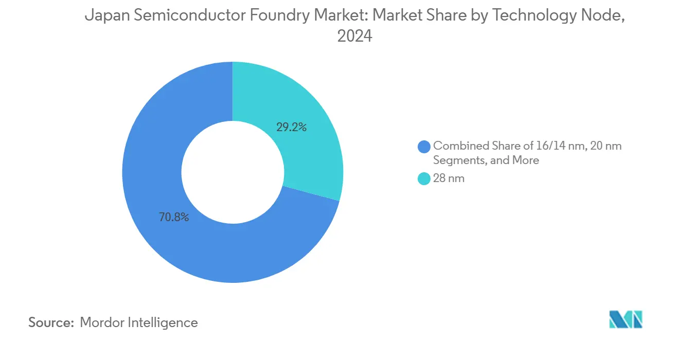
- By technology node, 28 nm held 29.2% of the Japan semiconductor foundry market share in 2024, while 10/7/5 nm and below is projected to compound at 25.4% through 2030.
- By wafer size, the 300 mm category accounted for 71.4% of the Japan semiconductor foundry market size in 2024 and is forecast to advance at a 23.8% CAGR during 2025-2030.
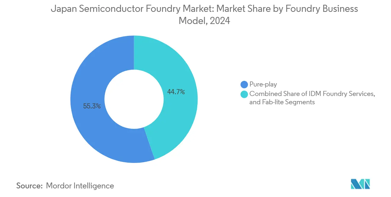
- By business model, pure-play operators commanded a 55.3% share of the Japan semiconductor foundry market size in 2024 and are set to grow at a 22.6% CAGR to 2030.
- By application, automotive devices led with 34.2% revenue share in 2024; high-performance computing is progressing at a 27.4% CAGR through 2030.
Japan contributes to a system defined not by any single country or region but by the interaction of many. The global semiconductor foundry market data by Mordor Intelligence represents that combined structure.
Japan Semiconductor Foundry Market Trends and Insights
Drivers Impact Analysis*
| Driver | (~) % Impact on CAGR Forecast | Geographic Relevance | Impact Timeline |
|---|---|---|---|
| Domestic 2 nm-class roadmap acceleration | +4.2% | Japan; Asia-Pacific spillover | Medium term (2-4 years) |
| Government subsidy surge for advanced-node fabs | +3.8% | National, Kumamoto, and Hokkaido | Short term (≤2 years) |
| Automotive safety-IC boom (EV/ADAS) | +3.5% | Global; Japan OEMs | Long term (≥4 years) |
| Edge-AI chip proliferation in consumer devices | +2.9% | Global; Japan CE makers | Medium term (2-4 years) |
| Supply-chain re-shoring incentives | +2.1% | Japan; allied nations | Long term (≥4 years) |
| Chiplet and 3D-IC packaging synergies | +1.8% | Global; Japan materials firms | Long term (≥4 years) |
| Source: Mordor Intelligence | |||
Domestic 2 nm-class roadmap acceleration
Rapidus inaugurated its IIM-1 fab in April 2025 and is shipping 2 nm samples by mid-year, bypassing 3 nm entirely to match TSMC and Samsung at the frontier.[1]Cliff Venzon, “Japan Outspends U.S., Germany on Chip Subsidies as Share of GDP,” Nikkei Asia, asia.nikkei.com Single-wafer processing triples cycle speed, enabling quick iteration for AI and HPC customers willing to pay a premium for shorter tape-out-to-silicon windows. IBM’s process IP transfer under the Economic Security Promotion Act de-risks technology ramp, while public grants covering >45% of capex cushion early yield volatility. Customer pre-payments from global fabless houses help underwrite pilot capacity, positioning Japan for first-mover advantage in sub-3 nm outsourcing.
Government subsidy surge for advanced-node fabs
The national semiconductor package reached JPY 3.9 trillion (USD 26 billion) between 2021-2023, equal to 0.71% of GDP and outstripping U.S. and German ratios. Up-front cash grants are paired with tax credits, loan guarantees, and expedited permitting that cut effective build cost by up to 40%. TSMC’s first Kumamoto plant received JPY 1.2 trillion (USD 8 billion) and began risk production 20 months after groundbreaking, a record for greenfield 300 mm fabs. Performance-based tranches link subsidies to volume, headcount, and technology transfer milestones, ensuring quantifiable domestic spillovers.
Automotive safety-IC boom (EV/ADAS)
Japan hosts eight of the world’s ten largest auto OEMs, all moving toward centralized, software-defined architectures that require 28 nm-to-7 nm logic and SiC power dies. The global automotive compute pool is rising 6% annually to USD 148 billion by 2030, and local foundries translate that into steady tape-ins for MCU, radar, lidar, and power management devices. Denso and Rohm’s May 2025 alliance bundles analog expertise with next-generation wafer capacity, while public subsidies of JPY 70.5 billion (USD 470 million) catalyze SiC expansion for 310,000 wafers a year. Qualification regimes such as AEC-Q100 prolong revenue visibility and support premium ASPs.
Edge-AI chip proliferation in consumer devices
Sony’s LYT-828 sensor, released June 2025, embeds on-chip HDR and neural processing in a 16 nm CIS flow, illustrating demand for low-power AI blocks in image pipelines. Domestic design start-ups like Preferred Networks target sub-10 W inference ASICs by 2027, reinforcing order flow for specialty processes optimized for SRAM density and voltage scaling. Japan’s proximity to camera, console, and appliance OEMs compresses logistics and fosters collaborative design reviews, accelerating ramp-to-volume relative to offshore foundries.
Restraints Impact Analysis*
| Restraint | (~) % Impact on CAGR Forecast | Geographic Relevance | Impact Timeline |
|---|---|---|---|
| Chronic shortage of experienced fab engineers | -2.7% | National, Kumamoto, and Hokkaido | Short term (≤2 years) |
| Elevated energy costs vs. peer geographies | -1.9% | National | Medium term (2-4 years) |
| Slow customer qualification cycle for new nodes | -1.4% | Global impact on Japan | Medium term (2-4 years) |
| Rising CapEx amid yen depreciation | -1.2% | National | Short term (≤2 years) |
| Source: Mordor Intelligence | |||
Chronic shortage of experienced fab engineers
Demand for 88,000 additional specialists by 2029 far exceeds the output of domestic universities, pressuring wage structures and stretching ramp schedules. TSMC broadened its Kumamoto University program in April 2024, but four-year graduation lags keep vacancy ratios near double digits. Rapidus foresees headcount growth from 150 to 2,000 engineers by 2027 and already recruits overseas talent at 30-40% pay premiums. Talent scarcity slows process debug, raises overtime expenses, and fuels poaching cycles that destabilize smaller peers.
Elevated energy costs vs. peer geographies
Japan’s industrial power tariff is roughly 50% above Taiwan’s, inflating per-wafer costs, especially for EUV-heavy nodes that pull >100 MWh per day.[2]TrendForce Analysts, “TSMC and PSMC Face Dilemma as Overseas Foundry Costs Skyrocket,” TrendForce, trendforce.com TSMC warns of 15-25% higher die pricing for output fabricated outside Taiwan, compelling OEMs to weigh geographic resilience against BOM inflation. Renewable-power build-outs could compress tariffs post-2030, but interim exposure erodes gross margins and challenges ROI assumptions on subsidy-backed projects.
*Our forecasts treat driver/restraint impacts as directional, not additive. The impact forecasts reflect baseline growth, mix effects, and variable interactions.
Segment Analysis
By Technology Node: Advanced Nodes Drive Premium Pricing
Japan semiconductor foundry market share for the 28 nm tier was 29.2% in 2024, because its cost-performance sweet spot aligns with automotive, MCU, and industrial ASIC use cases. Legacy traction remains durable, yet the 10/7/5 nm-and-below cohort is forecast to post a 25.4% CAGR and cross USD 2.4 billion by 2030 as AI inference and high-bandwidth computing workloads migrate to domestic capacity. TSMC’s second Kumamoto line will add 6/7 nm in 2027, giving OEMs a local option for sub-10 nm sourcing. Rapidus expects 50% initial yields at 2 nm, ramping to 90% over two years, pushing wafer-level cost parity with offshore peers once volumes stabilize.
Mature 45/40 nm and 65 nm platforms continue to serve power discretes and sensor interface ICs, but state incentives increasingly channel capex toward nodes capable of integrating RF, logic, and memory on a single die. Domestic fabs exploit co-optimization with next-generation ABF substrates and panel-level packaging to extract incremental die-size savings. While the Japan semiconductor foundry market retains healthy margins on nodes above 28 nm, the strategic narrative now centers on leapfrog entry into extreme scaling to secure future-proof production for allied customers.


By Wafer Size: 300 mm Dominance Reflects Efficiency Focus
The 300 mm category captured 71.4% of Japan's semiconductor foundry market share in 2024 and is advancing at a 23.8% CAGR as economies of scale drive per-die costs down roughly 35% relative to 200 mm lines. All new subsidy-qualified fabs mandate 300 mm equipment sets, concentrating advanced process migration on a single platform. Capacity tightness in legacy 200 mm fabs nevertheless sustains premium pricing for discrete power and analog flows, safeguarding utilization >95% through 2027.
Japan’s historic leadership in specialty 200 mm lines—covering nearly one-third of global output—remains relevant for SiC, GaN, and mixed-signal devices that prioritize voltage or thermal tolerances over transistor density. Select <150 mm capacity persists for high-voltage, niche sensor, and research wafers, though its revenue share drops below 2% by decade-end. Sustained 300 mm capex is accelerating automation adoption, water-reclaim systems, and clean-room modularity, reinforcing the cost base underpinning the Japan semiconductor foundry market.
By Foundry Business Model: Pure-Play Ascendant
Pure-play operators controlled 55.3% of the Japan semiconductor foundry market size in 2024, as fabless and IDM customers seek neutral partners free of downstream product conflicts. The model benefits from asset-light customers eager to decouple design and fabrication, enabling high utilization and diversified order books. Rapidus embodies this shift, drawing pre-payments from U.S. and European chip designers while pledging technology transparency and flexible IP arrangements.
IDM foundry services still command deep automotive and industrial linkages, with Sony, Renesas, and Toshiba incrementally opening spare capacity to third parties. Such hybrids offer bundled design-for-manufacturing support but may face internal allocation trade-offs under peak demand. Fab-lite configurations round out the landscape, allowing companies to keep advanced R&D in-house while outsourcing volume. Collectively, business-model pluralism bolsters resiliency, yet the pure-play cohort’s scale efficiencies and specialist focus continue to outpace rivals on both cost and time-to-yield, reinforcing its lead within the Japan semiconductor foundry market.
By Application: Automotive Leadership Drives Market Growth
Automotive electronics generated 34.2% of Japan's semiconductor foundry market size in 2024, underpinned by advanced driver assistance, electrified powertrains, and zonal controllers that multiply silicon content per vehicle. Full-stack OEM ecosystems facilitate co-development, streamlining PPAP and ISO 26262 compliance cycles. Rising demand for SiC, GaN, and high-current analog extends revenue visibility beyond logic scaling.
High-performance computing is the fastest-growing slice at a 27.4% CAGR, fueled by generative-AI inference, industrial digital twins, and smart-factory deployments that favor on-premise acceleration. Consumer electronics and communications maintain a steady share through camera upgrades and 5G/6G radio front-ends, while the industrial/IoT tranche benefits from brownfield digitalization grants that encourage onshore silicon sourcing. Niche fields such as aerospace, medical, and energy storage adopt Japan’s stringent quality and reliability pedigree, further diversifying the application ledger within the Japan semiconductor foundry market.
Geography Analysis
Japan’s domestic capacity confers strategic insulation from maritime chokepoints and geopolitical flashpoints that affect Taiwan and the South China Sea. Kumamoto Prefecture has emerged as the southern nucleus, hosting TSMC’s operational line since February 2024 and a second fab slated for 2027 completion, catalyzing more than 20 tier-one supplier investments in chemicals, gases, and specialty parts. Land prices in surrounding industrial parks climbed 10% year-over-year in 2024 as ancillary service providers secured plots.
Hokkaido anchors the northern pole with Rapidus’s Chitose campus focused on sub-3 nm R&D and risk production, enriching a regional talent pool long known for precision machinery and photonics. Central Honshu integrates legacy 200 mm and sub-28 nm lines, supplying automotive clusters in Aichi and Shizuoka. Government infrastructure grants fund grid upgrades and river-water purification plants to handle >5,000 ton-per-day fab loads, mitigating capacity constraints noted in early site surveys.[3]Staff Reporter, “Land, Water Supply Now Biggest Issue for Building New Wafer Fabs in Japan,” DIGITIMES Asia, digitimes.com
Japan’s alignment with the U.S.-led Chip 4 framework accelerates equipment import clearance and joint R&D on lithography, materials, and security standards, reassuring overseas customers of long-run policy stability. At the same time, export-control updates circumscribe sensitive node shipments to designated partners, reinforcing trust while preserving strategic autonomy. These geographic and policy vectors intertwine to underpin the robust expansion trajectory of the Japan semiconductor foundry market.
The semiconductor foundry market is analyzed by Mordor Intelligence across multiple other geographies. This is complemented by country-specific insights for South Korea, China, Taiwan, Singapore, Germany, United States, Malaysia, and Israel, reflecting various localized market behavior and policy environments' coverage.
Competitive Landscape
Competitive intensity is rising yet remains moderately fragmented, with the top five suppliers accounting for roughly 62% of national output. TSMC’s presence validates the addressable demand pool and raises process-yield benchmarks, prompting domestic incumbents to refresh tooling and embrace advanced packaging. Sony and Renesas leverage long-standing auto-sensor and MCU portfolios to secure block orders, while Toshiba pivots to SiC and GaN discretes aimed at powertrain inverters.
Alliances proliferate: Denso-Rohm integrates design and wafer capacities for ADAS SOCs, and Mazda-Rohm co-develops GaN motor-drive modules. Materials specialists strengthen vertical depth; AGC expands glass-core substrate output by 50% by 2030 to capture chiplet interposer demand.[4]AGC Corporate Communications, “The Japanese Glass Behind Next-Generation Chips,” agc.comDiamond semiconductor R&D led by Orbray and Saga University targets commercial power devices late in the decade, potentially unlocking sub-100 mΩ losses for EV drivetrains.
Foreign entrants operate under Japanese employment norms and quality audits, which temper culture-clash risks but elevate HR overhead. Scale, process breadth, and customer co-design capabilities emerge as primary differentiation levers, more so than absolute capacity. This competitive mosaic sustains innovation velocity and customer optionality within the Japan semiconductor foundry market.
Japan Semiconductor Foundry Industry Leaders
-
Sony Semiconductor Solutions Corp.
-
Renesas Electronics Corp.
-
United Semiconductor Japan Co., Ltd. (UMC)
-
TSMC Japan 3DIC R&D Center, Inc.
-
Tower Partners Semiconductor Co., Ltd. (TPSCo)
- *Disclaimer: Major Players sorted in no particular order

Recent Industry Developments
- August 2025: Rohm Semiconductor launched next-generation SiC MOSFETs ahead of schedule to counter Chinese rivals despite an 80% plunge in FY1Q operating profit.
- July 2025: Kioxia began mass production of ninth-generation NAND flash at Yokkaichi, targeting AI server storage.
- June 2025: Sony Semiconductor Solutions released the LYT-828 CMOS image sensor with >100 dB dynamic range; mass output starts Aug 2025.
- June 2025: Renesas postponed its USD 20 billion revenue target to 2035 and reduced power-chip capex after EV demand setbacks.


Japan Semiconductor Foundry Market Report Scope
| 10/7/5 nm and below |
| 16/14 nm |
| 20 nm |
| 28 nm |
| 45/40 nm |
| 65 nm and above |
| 300 mm |
| 200 mm |
| <150 mm |
| Pure-play |
| IDM Foundry Services |
| Fab-lite |
| Consumer Electronics and Communication |
| Automotive |
| Industrial and IoT |
| High-Performance Computing (HPC) |
| Other Applications |
| By Technology Node | 10/7/5 nm and below |
| 16/14 nm | |
| 20 nm | |
| 28 nm | |
| 45/40 nm | |
| 65 nm and above | |
| By Wafer Size | 300 mm |
| 200 mm | |
| <150 mm | |
| By Foundry Business Model | Pure-play |
| IDM Foundry Services | |
| Fab-lite | |
| By Application | Consumer Electronics and Communication |
| Automotive | |
| Industrial and IoT | |
| High-Performance Computing (HPC) | |
| Other Applications |


Key Questions Answered in the Report
How large is the Japan semiconductor foundry market in 2025?
It stands at USD 3.3 billion and is on track to reach USD 7.8 billion by 2030.
What CAGR is forecast for Japan’s foundry revenues to 2030?
Revenues are projected to grow at an 18.8% CAGR during 2025-2030.
Which technology node currently contributes the most revenue?
The 28 nm node leads with 29.2% share of 2024 sales.
Why are automotive customers central to Japanese foundry growth?
Electrification and ADAS adoption push vehicle OEMs to source high-reliability logic and SiC power dies locally, giving automotive 34.2% of 2024 revenue.
What is Japan’s main competitive challenge against Taiwan?
Higher electricity tariffs raise per-wafer costs by about 50%, prompting 15-25% die price premiums for Japan-made chips.
How much public money supports new fabs?
Government subsidies totaled JPY 3.9 trillion (USD 26 billion) between 2021 and 2023, with additional tranches earmarked for 2025 projects.
Page last updated on:


