South Korea Semiconductor Foundry Market Size and Share
Market Overview
| Study Period | 2019 - 2030 |
|---|---|
| Forecast Data Period | 2025 - 2030 |
| Historical Data Period | 2019 - 2023 |
| Market Size (2025) | USD 23.10 Billion |
| Market Size (2030) | USD 33.80 Billion |
| Growth Rate (2025 - 2030) | 7.90% CAGR |
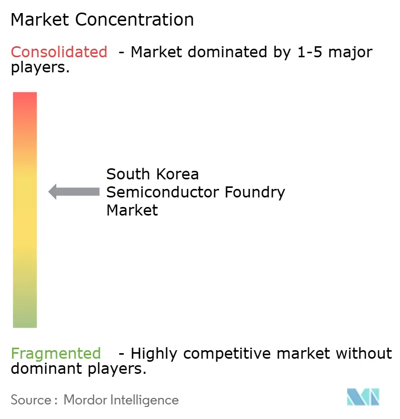
| Market Concentration | Medium |
Major Players
*Disclaimer: Major Players sorted in no particular order Image © Mordor Intelligence. Reuse requires attribution under CC BY 4.0. |
|
South Korea Semiconductor Foundry Market Analysis by Mordor Intelligence
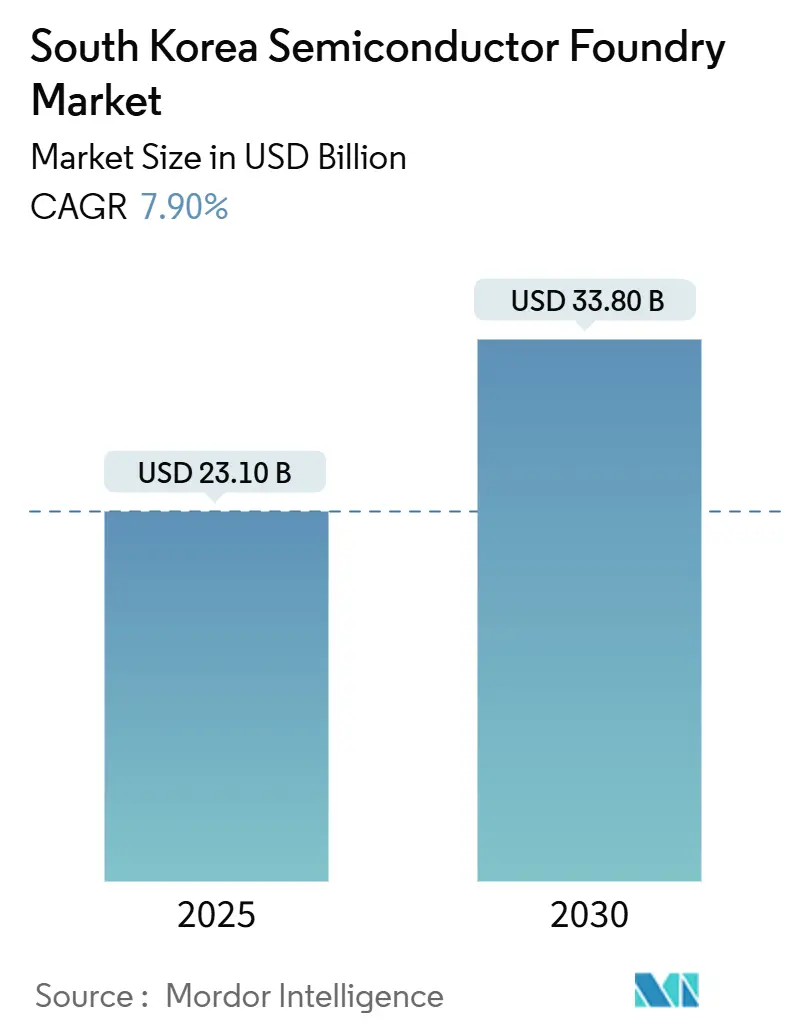
The South Korean semiconductor foundry market size stands at USD 23.1 billion in 2025 and is forecast to reach USD 33.8 billion by 2030, registering a 7.9% CAGR. Continued migration to advanced nodes, robust policy support, and diversified demand from artificial intelligence, electric vehicles, and next-generation wireless devices are sustaining the uptrend. Government incentives under the K-SEMICON Act have lowered capital hurdles, while strategic mega-cluster projects in Gyeonggi Province are expanding domestic capacity. Foundry pricing power is firm because sub-10 nm lines remain more than 90% utilized, and demand for heterogeneous integration is pushing service differentiation. At the same time, export-control risk and local water-use limits inject supply-side uncertainty that management teams actively hedge through overseas fabs and ESG investment.
Key Report Takeaways
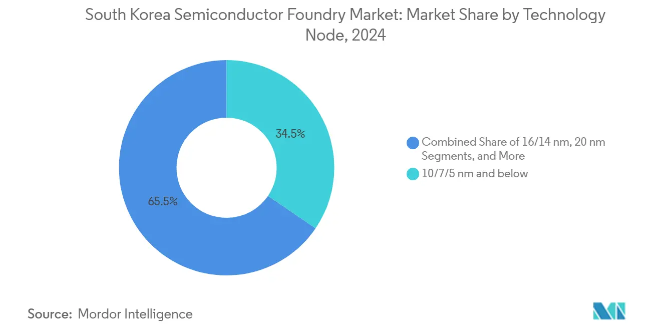
- By technology node, the ≤7 nm category accounted for 34.5% of South Korea's semiconductor foundry market share in 2024 and is advancing at a 10.5% CAGR through 2030.
- By wafer size, 300 mm substrates captured 75.2% of the South Korean semiconductor foundry market size in 2024 and are projected to expand at a 9.8% CAGR to 2030.
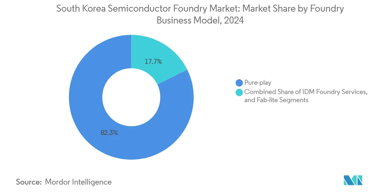
- By business model, pure-play operators held 82.3% revenue share in 2024, while IDM foundry services are the fastest-growing at an 8.7% CAGR through 2030.
- By application, high-performance computing posted the strongest outlook with an 11.4% CAGR, even as consumer electronics retained a 40.6% revenue share in 2024.
Proportional positioning is established by comparing country level and regional contributions against the global total, including that of South korea. The semiconductor foundry market share in our global report expresses these relative weights.
South Korea Semiconductor Foundry Market Trends and Insights
Drivers Impact Analysis*
| Driver | (~) % Impact on CAGR Forecast | Geographic Relevance | Impact Timeline |
|---|---|---|---|
| Surging demand for ≤7 nm nodes in AI and HPC | +2.8% | Global, concentrated in Asia-Pacific | Medium term (2-4 years) |
| Government incentives under the K-SEMICON Act | +1.9% | National, with spillover to global supply chains | Long term (≥ 4 years) |
| Automotive semiconductor demand (EV/ADAS) | +1.4% | Global, early gains in Korea, Europe, and North America | Medium term (2-4 years) |
| 5G/6G consumer-device refresh cycles | +0.9% | Global, led by Asia-Pacific markets | Short term (≤ 2 years) |
| Chiplet-based heterogeneous integration boom | +0.7% | Global, concentrated in advanced manufacturing hubs | Long term (≥ 4 years) |
| Hydrogen-powered fabs for ESG cost edge | +0.3% | National, potential expansion to developed markets | Long term (≥ 4 years) |
| Source: Mordor Intelligence | |||
Surging Demand for ≤7 nm Nodes in AI and HPC
Hyperscale operators continue to lock in long-term capacity agreements as data-center rollouts require higher-density AI accelerators. Samsung reported an 80% year-over-year jump in AI-related foundry revenue in 2024 and targets a ninefold rise in AI chip sales by 2028.[1]Samsung Electronics, “Samsung Showcases AI-Era Vision and Latest Foundry Technologies at SFF 2024,” News.Samsung.com, news.samsung.com Back-side power-delivery networks entering the SF2Z node roadmap will lift performance per watt, reinforcing demand visibility. Sustained utilization above 90% in sub-10 nm lines keeps pricing resilient and supports a favorable mix shift toward premium wafers. Geographic clustering of data-center builds in Korea, Japan, and Singapore adds some volume volatility because a single hyperscaler decision can swing multi-percentage-point loads. However, contractual take-or-pay clauses limit downside risk and anchor the South Korean semiconductor foundry market.
Government Incentives under the K-SEMICON Act
National tax credits for R&D have been raised to as much as 50%, while investment credits now reach 25%, significantly reducing project breakeven points. A KRW 150 trillion financing pool over three years backs fab expansions and equipment procurement. Fast-track permitting around the Yongin mega-cluster cuts infrastructure lead times, giving Korea an edge over new-build sites in the United States and Europe. Localization goals that target 50% self-sufficiency in critical inputs by 2030 enhance supply resilience and encourage material producers to co-locate plants inside the cluster. Labor availability also benefits from coordinated talent pipelines between universities and fab operators, further consolidating the South Korean semiconductor foundry market.
Automotive Semiconductor Demand (EV/ADAS)
Electrification is lifting silicon content per vehicle as power-train inverters, battery-management ICs, and zonal controllers migrate to 28 nm and below. Hyundai publicly committed to selling 3.62 million zero-emission vehicles by 2030, creating a domestic anchor customer for new automotive-grade nodes. Samsung aims for automotive contracts to reach a 30% revenue mix by 2028, leveraging advanced packaging that combines ADAS and infotainment processors on a single substrate. Chiplet-based reference designs allow swift adaptation to changing OEM compute requirements, while stringent Automotive Safety Integrity Level (ASIL) standards raise qualification barriers for overseas competitors. These factors collectively extend the growth runway for the South Korean semiconductor foundry market.
5G/6G Consumer-Device Refresh Cycles
South Korean carriers led by SK Telecom commenced 6G field trials in early 2025, a move that accelerates chipset roadmaps for smartphones and wearables. Device makers are integrating on-device AI engines that require 3 nm gate-all-around (GAA) logic, as seen in Samsung’s Exynos W1000 smartwatch processor. Component orders typically tighten in the second half, flattening seasonality and allowing foundries to smooth tool maintenance schedules. While consumer electronics growth moderates compared with enterprise demand, refresh cycles still represent a high-volume baseline that stabilizes overall wafer starts, anchoring revenue visibility for the South Korean semiconductor foundry market.
Restraints Impact Analysis*
| Restraint | (~) % Impact on CAGR Forecast | Geographic Relevance | Impact Timeline |
|---|---|---|---|
| Cyclical memory downturn curbing capex | -1.6% | Global, concentrated in memory-focused regions | Short term (≤ 2 years) |
| US–China export controls on EUV tools | -1.2% | Global, particularly affecting advanced node capacity | Medium term (2-4 years) |
| Shortage of advanced lithography engineers | -0.8% | Global, acute in advanced manufacturing hubs | Long term (≥ 4 years) |
| Water-use restrictions in Gyeonggi province | -0.4% | National, with potential expansion to other manufacturing regions | Medium term (2-4 years) |
| Source: Mordor Intelligence | |||
Cyclical Memory Downturn Curbing Capex
DRAM and NAND prices weakened during 2024, prompting Samsung to halve foundry capital expenditure to KRW 5 trillion in 2025. Shared lithography and clean-room assets between memory and logic lines create allocation conflicts, delaying mature-node expansions that serve power-management ICs and analog devices. The ripple effect is felt most acutely by second-tier design houses that rely on flexible wafer slots. Though memory pricing is expected to rebound in 2026, the near-term funding pullback trims incremental capacity and slightly tempers the South Korean semiconductor foundry market growth trajectory.
US–China Export Controls on EUV Tools
The October 2024 tightening of U.S. export rules extended license reviews to South Korean fabs using extreme-ultraviolet equipment sourced from ASML.[2]Robert A. Friedman, “U.S. Strengthens Export Controls on Advanced Computing Items, Semiconductor Manufacturing Items,” HKLaw.com, hklaw.com New system deliveries now carry multi-quarter approval cycles, lengthening advanced-node ramp times and forcing operators to optimize existing toolsets. Maintenance and spare-part constraints also pose uptime risks that smaller fabs struggle to absorb. While Seoul’s strategic alliance with Washington has secured temporary waivers, ongoing geopolitical uncertainty inflates risk premiums on multi-billion-dollar fab projects, modestly weighing on South Korea's semiconductor foundry market expansion.
*Our forecasts treat driver/restraint impacts as directional, not additive. The impact forecasts reflect baseline growth, mix effects, and variable interactions.
Segment Analysis
By Technology Node: Advanced Nodes Capture Value
The 10/7/5 nm and below segment held 34.5% of the South Korean semiconductor foundry market share in 2024 and is on track for a 10.5% CAGR through 2030. Volume ramps for AI accelerators and data-center CPUs drive this leadership, with Samsung’s 2 nm GAA roadmap scheduled for initial production in 2025. The 16/14 nm tier remains a workhorse for automotive microcontrollers, while 28 nm serves IoT and DTV chips. Mature nodes above 45 nm continue to support analog and power-management ICs but face price competition from Chinese rivals. As cost per transistor flattens at cutting-edge nodes, design houses increasingly adopt chiplet architectures on 4 nm platforms to balance performance and yield. Process diversification, therefore, complements pure scaling, broadening margins across node buckets and underpinning the South Korea semiconductor foundry market size outlook.
Complementing the node mix, complexity per wafer keeps rising—back-side power-delivery and buried power rails enter risk production by 2027, pushing mask counts past 120 layers. Tool suppliers coordinate closely with fabs to streamline process steps, and early adopters secure premium wafer-pricing arrangements. Consequently, the ≤7 nm tier will account for a disproportionate share of the absolute profit pool even as older nodes retain volume relevance.


By Wafer Size: 300 mm Dominance Deepens
The 300 mm format commanded 75.2% of the South Korean semiconductor foundry market size in 2024 and is growing at a 9.8% CAGR through 2030. Scale economics make 300 mm the baseline for sub-20 nm geometries, and depreciation schedules encourage consolidation of mature process flows onto larger substrates. SK Hynix broke ground on a USD 6.8 billion 300 mm complex in Yongin in July 2024. Meanwhile, 200 mm capacity stays relevant for image sensors and power semiconductors where die footprints are small. Experimental 450 mm work benches remain in R&D because of equipment cost and supply-chain readiness lag. As mask-set prices near USD 700,000 for 7 nm designs, the cost advantage of larger wafers becomes critical, reinforcing the centrality of 300 mm and locking in its share above 70% of the South Korean semiconductor foundry market.
By Foundry Business Model: Pure-Play Trust Advantage
Pure-play specialists captured 82.3% of 2024 revenue and are forecast to expand at an 8.7% CAGR to 2030. Customers prize the “no-compete” stance and deep ecosystem support that dedicated manufacturers provide. Samsung’s hybrid role as both designer and foundry introduces potential IP-sharing friction, prompting certain fabless clients to pursue multi-sourcing strategies. IDMs' opening excess capacity to external customers adds supply but still trails pure-plays in design-service breadth. Fab-lite models fill tactical gaps for firms upgrading specific process steps without committing to full foundry status. These dynamics collectively strengthen the contract-manufacturing ethos that underpins the South Korean semiconductor foundry market.
By Application: HPC Surges Ahead
High-performance computing overtook other categories with an 11.4% CAGR forecast to 2030, propelled by AI training, inference, and cloud acceleration workloads. Samsung aims to lift HPC-linked wafer starts from 19% in 2024 to 45% by 2028. Consumer electronics still contributed 40.6% revenue share in 2024, yet growth has plateaued as smartphone penetration nears saturation. Automotive silicon demand accelerates on the back of centralized compute architecture and safety-critical sensor fusion, while industrial IoT drives steady 28 nm and 40 nm volume. The rising weight of enterprise customers signals a structural shift in the South Korean semiconductor foundry market toward higher-value, lower-seasonality business.
Geography Analysis
South Korea generated approx. 13.2% of global semiconductor revenue in 2023, providing a robust domestic customer base for foundry operators. The Hwaseong–Pyeongtaek corridor clusters memory and logic production, allowing wafer-transport efficiencies and shared utilities. Government-backed mega-clusters promise 7.7 million wafers per month of incremental capacity by 2030. This integrated setup reduces supply-chain latency for photoresist, specialty gases, and advanced substrates, giving the South Korean semiconductor foundry market a tangible cost advantage.
Export-control policies, however, compel companies to diversify footprints. Samsung secured USD 4.745 billion in CHIPS Act incentives for its Taylor, Texas fab, slated for 2026 operation, partly to safeguard U.S. customer access. As U.S. and Japanese subsidies lure future lines abroad, Korea’s global share could edge down to 10% by 2027, yet local fabs remain preferred for R&D pilot lots and early-node ramp-ups. Water scarcity in Gyeonggi Province looms as a structural constraint; semiconductor water demand is set to double by 2035, mandating reclaimed-water projects and piping upgrades.[3]Silicon Semiconductor News, “Water Usage in Semiconductor Manufacturing to Double by 2035,” siliconsemiconductor.net Municipal agencies plan tiered pricing to encourage recycling, and fabs are testing hydrogen-powered boilers to cut both carbon and freshwater intensity.
Regional geopolitics injects dual-sided risk. Seoul’s security alliance with Washington ensures technology access but also entangles Korea in U.S.–China trade friction. Conversely, Korean design startups such as FuriosaAI have begun rejecting foreign acquisition overtures to keep IP local, signaling a confidence that reinforces national innovation depth. The net effect is a measured yet resilient trajectory for the South Korean semiconductor foundry market.
Mordor Intelligence examines the semiconductor foundry market across diverse other regional markets as well, offering granular country-level perspectives for Malaysia, Taiwan, Japan, Singapore, Germany, China, United States, and Israel and more.
Competitive Landscape
Market concentration is moderate: Samsung held a significant share of global foundry share in 2024 but leads domestically, while foreign majors operate local packaging or test centers rather than full logic fabs. Yield hurdles at 3 nm GAA nodes have delayed some customer tape-outs, but aggressive process-control improvements narrowed the gap with peer leaders during 2025. Differentiation centers on back-side power-delivery, multi-die integration, and advanced packaging. Samsung’s SAINT-D 3D HBM platform directly competes with TSMC’s CoWoS for AI accelerator stacking.[4]Samsung Electronics, “Samsung Showcases AI-Era Vision and Latest Foundry Technologies at SFF 2024,” News.Samsung.com, news.samsung.com
Strategic alliances multiply: Intel and Samsung began exploratory talks on reciprocal capacity support for 18 Å and 2 nm nodes, a sign of tightening tool-availability constraints and shared interest in counterbalancing TSMC. Meanwhile, SK Hynix’s substantive investment in Yongin anchors future memory-logic integration plays, offering local design houses novel “logic-plus-HBM” service bundles that could gain traction with AI chiplets. Domestic fabless firms receive growing venture backing, and Hyundai’s stake in BOS Semiconductors underscores automotive verticalization goals.
Advanced packaging capacity has emerged as a new bottleneck. Line-time for 2.5D interposers approaches full allocation through mid-2026, and Samsung is scaling its I-Cube roadmap to capture incremental demand. Tool-lead-time risk and expertise scarcity in hybrid bonding create switching costs that raise industry barriers, reinforcing incumbency and supporting margins across the South Korean semiconductor foundry market.
South Korea Semiconductor Foundry Industry Leaders
-
Samsung Electronics Co., Ltd. (Samsung Foundry Division)
-
SK Hynix System IC Inc.
-
DB HiTek Co., Ltd.
-
J-Devices Korea Co., Ltd.
-
Magnachip Semiconductor Corporation
- *Disclaimer: Major Players sorted in no particular order

Recent Industry Developments
- March 2025: FuriosaAI rejected Meta’s USD 800 million acquisition offer to continue independently developing AI inference chips.
- January 2025: Samsung Electronics reduced foundry investment by 50% to KRW 5 trillion (USD 4.02 billion) to focus on 2 nm yield enhancement.
- July 2024: SK Hynix’s board approved a USD 6.8 billion 300 mm memory-fab project in Yongin, with construction starting in 2025 and completion targeted for 2027.
- June 2024: Samsung Electronics introduced SAINT-D HBM4 packaging service aimed at AI GPUs, claiming 20% power reduction and improved signal integrity.


South Korea Semiconductor Foundry Market Report Scope
| 10/7/5 nm and below |
| 16/14 nm |
| 20 nm |
| 28 nm |
| 45/40 nm |
| 65 nm and above |
| 300 mm |
| 200 mm |
| <150 mm |
| Pure-play |
| IDM Foundry Services |
| Fab-lite |
| Consumer Electronics and Communication |
| Automotive |
| Industrial and IoT |
| High-Performance Computing (HPC) |
| Other Applications |
| By Technology Node | 10/7/5 nm and below |
| 16/14 nm | |
| 20 nm | |
| 28 nm | |
| 45/40 nm | |
| 65 nm and above | |
| By Wafer Size | 300 mm |
| 200 mm | |
| <150 mm | |
| By Foundry Business Model | Pure-play |
| IDM Foundry Services | |
| Fab-lite | |
| By Application | Consumer Electronics and Communication |
| Automotive | |
| Industrial and IoT | |
| High-Performance Computing (HPC) | |
| Other Applications |


Key Questions Answered in the Report
How large is the South Korean semiconductor foundry market in 2025?
The South Korean semiconductor foundry market size is USD 23.1 billion in 2025.
What is the projected CAGR for Korean foundry revenue to 2030?
Aggregate revenue is forecast to grow at a 7.9% CAGR through 2030.
Which technology node is expanding the quickest?
The ≤7 nm node segment is growing the fastest at a 10.5% CAGR to 2030.
Why do 300 mm wafers dominate Korean production?
They offer superior cost-per-die economics for advanced nodes and thus hold over 75% market share in 2024.
How will export controls affect new Korean fabs?
Longer approval cycles for EUV tools could delay sub-7 nm ramps and modestly trim near-term capacity growth.
What role does automotive demand play in foundry growth?
Electrification and ADAS are lifting chip content per vehicle, driving a 1.4 percentage-point positive impact on overall CAGR.
Page last updated on:


