China Semiconductor Foundry Market Size and Share
Market Overview
| Study Period | 2019 - 2030 |
|---|---|
| Forecast Data Period | 2025 - 2030 |
| Historical Data Period | 2019 - 2023 |
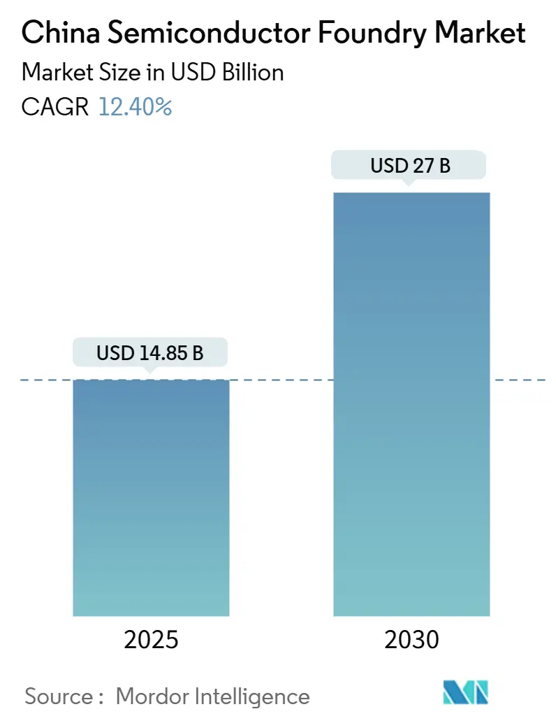
| Market Size (2025) | USD 14.85 Billion |
| Market Size (2030) | USD 27 Billion |
| Growth Rate (2025 - 2030) | 12.40% CAGR |
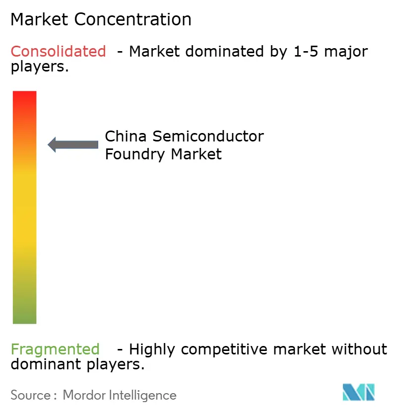
| Market Concentration | High |
Major Players
*Disclaimer: Major Players sorted in no particular order Image © Mordor Intelligence. Reuse requires attribution under CC BY 4.0. |
|
China Semiconductor Foundry Market Analysis by Mordor Intelligence
The China semiconductor foundry market size stands at USD 14.85 billion in 2025 and is forecast to reach USD 27 billion by 2030, advancing at a 12.4% CAGR. This growth outlook rests on Beijing’s large-scale capital subsidies, a rising domestic design ecosystem, and accelerating import-substitution across automotive, AI servers, and power electronics.[1]South China Morning Post, “China gave 190 chip firms US$1.75 billion in subsidies in 2022 as it seeks semiconductor self-sufficiency,” scmp.com Heightened geopolitical friction has redirected orders from multinational clients toward local fabs, while state-backed equipment makers shave procurement costs and shorten ramp-up cycles. Demand for mature-node production remains resilient, especially for 28 nm processes for vehicle control units, power management ICs, and IoT chipsets. Parallel investments into silicon-carbide and gallium-nitride power devices diversify revenue streams and position Chinese suppliers for the new-energy vehicle surge. The supply-side response is visible in four 12-inch fabs under construction by the country’s flagship foundry and in province-level mega projects across the Yangtze River Delta and the Greater Bay Area.
Key Report Takeaways
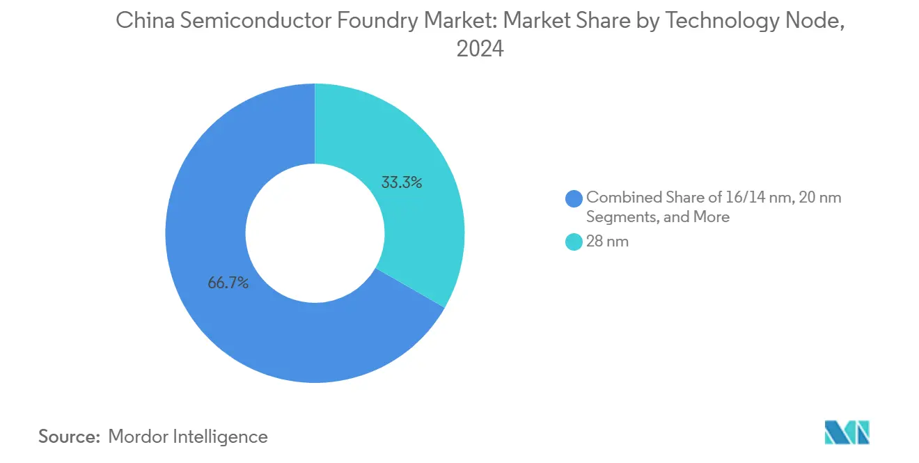
- By technology node, 28 nm held 33.3% of the China semiconductor foundry market share in 2024, while sub-10 nm nodes are projected to expand at an 18.2% CAGR through 2030.
- By wafer size, 300 mm substrates commanded 62.6% share of the China semiconductor foundry market size in 2024 and are expected to grow at a 10.5% CAGR up to 2030.
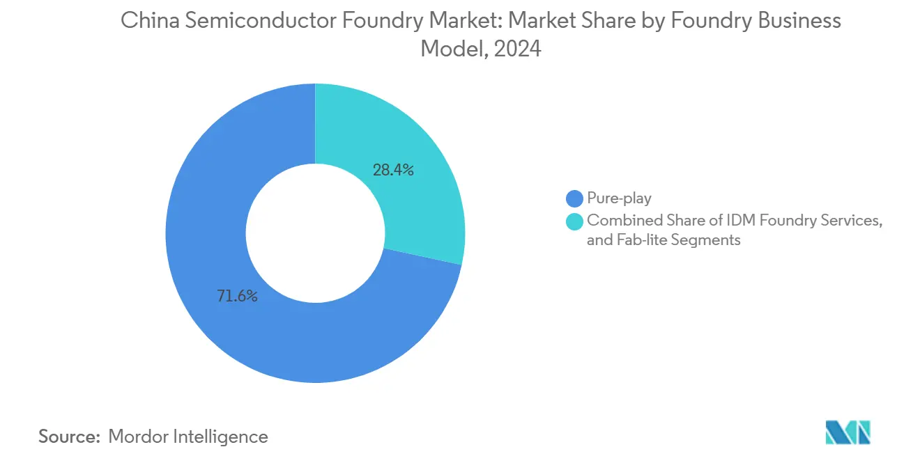
- By business model, pure-play foundries led with 71.6% revenue share in 2024, whereas IDM foundry services exhibit the highest forecast CAGR of 12.1% through 2030.
- By application, automotive chips accounted for 15.7% CAGR, the fastest pace among end markets, supported by electric-vehicle penetration topping 50% of new car sales in July 2024.
Future direction is shaped by developments occurring across multiple countries and regions, with China contributing to the overall trajectory. The outlook on worldwide semiconductor foundry market reflects how these are expected to evolve collectively.
China Semiconductor Foundry Market Trends and Insights
Drivers Impact Analysis*
| Driver | (~) % Impact on CAGR Forecast | Geographic Relevance | Impact Timeline |
|---|---|---|---|
| Government incentives and “Made-in-China 2025” capital subsidies | +2.8% | National: Yangtze River Delta and Greater Bay Area | Long term (≥ 4 years) |
| Surging demand for mature-node chips (28 nm +) from automotive/IoT | +2.1% | Global demand, domestic production | Medium term (2-4 years) |
| Localization push for SiC and GaN power devices | +1.7% | National: Wuhan, Changsha, Yiwu | Medium term (2-4 years) |
| AI server boom requiring domestic packaging/foundry synergy | +1.9% | Global AI demand, local build-out | Short term (≤ 2 years) |
| Emergence of regional semiconductor clusters | +1.4% | Eastern China | Long term (≥ 4 years) |
| Rise of state-backed equipment makers lowering cap-ex barriers | +1.6% | Nationwide | Medium term (2-4 years) |
| Source: Mordor Intelligence | |||
Government incentives and “Made-in-China 2025” capital subsidies
R&D tax breaks and multi-level equity funds remain the single biggest accelerant for the China semiconductor foundry market. National IC funds, municipal subsidy pools, and preferential tax codes collectively produced USD 322 billion-equivalent in fiscal support between 2020 and 2024.[2]中国政府网, “2024年1—11月支持科技创新和制造业发展主要政策减税降费及退税约2.3万亿元,” gov.cn Firms operating at or below 28 nm enjoy five-year income-tax holidays followed by reduced brackets, cushioning initial losses and improving the internal rate of return. State councils also push bulk procurement of domestic tools and materials, driving volume orders for local lithography, etch, and deposition vendors. Shanghai’s Lingang New Area alone targets semiconductor output worth CNY 100 billion (USD 14.0 billion) by 2025 through bonded-zone incentives. The consistent subsidy pipeline lowers break-even thresholds, speeds fab build-outs, and underwrites long-dated technology-node R&D, forming the backbone of the market’s double-digit CAGR.
Surging demand for mature-node chips from automotive and IoT
Electric-vehicle architecture relies heavily on 28 nm–65 nm micro-controllers, power-management ICs, and gate drivers, all of which favor high-yield mature processes. With EV penetration already above 50% of new passenger cars, local fabs face steady wafer-start growth curves. Domestic auto OEMs now co-design chips with foundries to secure priority capacity. In parallel, a flourishing IoT hardware scene—from smart meters to wearables—continues to pull on 55 nm and 40 nm platforms. The China semiconductor foundry market, therefore, benefits from long product lifecycles and minimal design churn, producing stable gross-margin pools even as leading-edge nodes experience export-control headwinds. The mature-node wave compounds the market’s overall revenue base and dilutes cyclical risk.
Localization push for silicon-carbide and GaN power devices
Third-generation semiconductors are integral to 800-V EV drivetrains and fast-charging stations. Wuhan’s recently commissioned SiC wafer plant delivers 360,000 six-inch wafers annually, with first-pass yields topping 97%. San’an Optoelectronics is scaling another facility in Changsha for 180,000 wafers, while multiple provincial funds back GaN lines aimed at 5 G infrastructure. Local suppliers now quote wafers 30% under global benchmarks, accelerating domestic device adoption. For the China semiconductor foundry market, integrating SiC epitaxy and device fabrication diversifies product mixes and raises average selling prices, offsetting price compression in legacy nodes. Investment outlays also attract new customers from renewables and industrial-drive sectors, reinforcing loadings at conventional 6-inch and 8-inch fabs.
AI server boom requiring domestic packaging/foundry synergy
Large-language-model rollouts have amplified demand for high-bandwidth-memory stacks and chiplets requiring advanced packaging. Domestic foundries and outsourced assembly houses are co-locating 2.5-D interposer lines to eliminate import bottlenecks. Over USD 11.5 billion in cap-ex has flowed into local CoWoS-class equipment since 2023, supported by targeted grants and design wins from cloud majors. SMIC added 30,000 12-inch wafers per month in Q4 2024 specifically for AI accelerators, while CXMT plots HBM3 production by 2026. Such vertical integration captures margin that previously accrued to offshore package-substrate vendors, inflating the top line of the China semiconductor foundry market and accelerating time-to-market for indigenous GPU initiatives.
Restraints Impact Analysis*
| Restraint | (~) % Impact on CAGR Forecast | Geographic Relevance | Impact Timeline |
|---|---|---|---|
| US export-control choke-points on EUV/advanced EDA tools | -3.2% | Global access gaps | Long term (≥ 4 years) |
| Over-capacity risk in mature nodes is causing ASP erosion | -1.8% | Global mature chip markets | Medium term (2-4 years) |
| Power-supply and water-use constraints in key hubs | -1.4% | Eastern China clusters | Long term (≥ 4 years) |
| Talent shortage amid aggressive fab build-outs | -2.1% | Nationwide | Medium term (2-4 years) |
| Source: Mordor Intelligence | |||
US export-control choke-points on EUV and advanced EDA tools
Washington’s 2024 rules widened the Entity List and imposed foreign-direct-product restrictions that now cover critical immersion DUV scanners and cutting-edge design software.[3]Holland and Knight, “U.S. Strengthens Export Controls on Advanced Computing Items, Semiconductor Manufacturing Items,” hklaw.com The clampdown blocks immediate access to EUV machines, delaying sub-7 nm capacity ramps inside China. Local toolmakers have responded with 28 nm-capable ArF immersion platforms, but these remain years behind global leaders. The policy drag is therefore most acute at the premium ASP end of the China semiconductor foundry market, shaving shipment potential for leading-edge logic and constraining domestic GPU supply. While multiyear R&D programs aim to localize the tool chain, revenue leakage toward foreign foundries will persist through the forecast horizon.
Over-capacity risk in mature nodes is causing ASP erosion
State-subsidized fabs could lift China’s share of global 28 nm–65 nm capacity toward 39% by 2027. Incentive-induced build-outs heighten the chance that wafer starts outrun end-market demand, pushing foundries to cut prices; SMIC already dropped 28 nm quotes from USD 2,500 to USD 1,500 per wafer during 2024’s down-cycle. While robust domestic consumption absorbs part of the glut, price competition remains a credible deflationary force on the Chinese semiconductor foundry market. Government planners may need to temper subsidy intensity or tighten project approvals to avoid sustained margin compression.
*Our forecasts treat driver/restraint impacts as directional, not additive. The impact forecasts reflect baseline growth, mix effects, and variable interactions.
Segment Analysis
By Technology Node: Mature Strength, Advanced Momentum
The 28 nm node delivered USD 4.9 billion, equal to 33.3% of the China semiconductor foundry market size in 2024, and continues to anchor automotive, industrial, and IoT workflows. With subsidies tailored to sub-28 nm, domestic fabs now aim for 31% of global 28 nm output by 2027, reinforcing pricing power in a node still mainstream for powertrain MCUs and connectivity chipsets. Meanwhile, sub-10 nm capacity remains nascent yet logs the highest 18.2% CAGR thanks to AI accelerator tape-outs and national research grants. SMIC’s quasi-7 nm DUV route indicates technical ingenuity amid tool embargoes, though true 5 nm remains outside the five-year window.
As capital intensity rises, foundries balance node migration with profitability. 16/14 nm platforms absorb logic refreshes from mobile SoCs, and 40/45 nm lines cater to analog mixed-signal devices. This layered strategy stabilizes fab utilization and broadens the revenue base, making technology diversification a structural pillar for the China semiconductor foundry market.


By Wafer Size: 300 mm Retains Scale Advantage
High-volume digital logic, memory, and CIS flows favor 12-inch substrates, granting 300 mm a dominant 62.6% slice of the China semiconductor foundry market share in 2024. Expansion projects in Beijing, Shanghai, Shenzhen, and Tianjin will lift the national 300 mm capacity by another 240,000 wafers per month after 2026. Economies of scale and automated material handling secure lower per-chip costs, sustaining a projected 10.5% CAGR for this segment.
The 200 mm tier remains vital for analog, MEMS, and embedded-flash nodes; it provides capacity for high-reliability parts where process stability trumps transistor density. ≤ 150 mm fabs, although niche, fill specialty demand for SiC, GaAs, and MEMS microphones. Targeted subsidies for third-generation semiconductors are reviving investment into 6-inch and 8-inch lines, ensuring multi-diameter resilience within the broader China semiconductor foundry market.
By Foundry Business Model: IDM Services Pick Up Pace
Pure-play suppliers still represent 71.6% of 2024 revenue and attract a broad customer roster of more than 1,000 design houses. The approach provides flexibility and scale, securing USD 2.2 billion in Q4 2024 sales for the market leader. Conversely, IDM foundry services are posting a 12.1% CAGR as vehicle OEMs vertically integrate silicon to mitigate supply shocks. BYD now fabricates 90% of its power electronics in-house, exemplifying the shift.
Fab-lite models give chip firms optionality in capital allocation, letting them retain pilot lines while outsourcing volume. The Chinese semiconductor foundry industry thus evolves into a spectrum—from pure-play to fully integrated—each addressing distinct risk-reward preferences among customers. This diversity underpins supply-chain resilience and tempers cyclical swings in the China semiconductor foundry market.
By Application: Automotive Leads Growth Curve
Consumer electronics maintained 38.8% of 2024 revenue, but automotive IC demand grows fastest at 15.7% CAGR as EV makers add power, ADAS, and infotainment controllers. Over 300 domestic auto-chip startups have been launched since 2023, ensuring a sustained tape-out pipeline. High-performance computing benefits from AI server clusters funded by cloud majors, while industrial and IoT devices continue to migrate to domestic sources amid government procurement directives.
App-level diversification shields the Chinese semiconductor foundry market from single-sector downturns. When smartphone silicon orders softened in 2024, automotive and data-center chips filled capacity, maintaining an 89.6% utilization rate for the leading fab. A balanced end-market mix, therefore, remains a strategic hedge for revenue stability and cap-ex justification.
Geography Analysis
China’s foundry footprint concentrates in three mega clusters. The Yangtze River Delta produces one-quarter of the national GDP and one-third of R&D expenditure within only 4% of the land area.[4]PricewaterhouseCoopers, “The Yangtze River Delta – China’s leading regional economic cluster,” pwc.de Shanghai anchors this belt with USD 41 billion in 2022 IC sales and a dedicated “Oriental Chip Port” blueprint for 2025. Neighboring Jiangsu excels in assembly and testing, while Zhejiang recruits SiC and GaN projects, forming a vertically integrated value chain.
The Greater Bay Area, led by Guangdong, offers proximity to electronics OEMs and access to Hong Kong’s capital pools. Province authorities committed CNY 500 billion (USD 70.0 billion) into 40 semiconductor ventures, including the region’s sole 300 mm fab capable of 80,000 wafers per month. Specialized fabs in Shenzhen and Zhuhai tackle RF front-end and display drivers, complementing consumer-device assemblers across the Pearl River Delta.
Northern hubs around Beijing leverage elite universities and national labs for cutting-edge R&D. Upcoming 12-inch fabs in the capital will bridge design talent with new equipment makers such as AMEC and Naura. Logistics corridors and water-supply projects aim to ease utility bottlenecks, while inland centers like Wuhan and Changsha absorb SiC-focused lines to diversify geographic risk. Collectively, these nodes foster a robust ecosystem that undergirds the long-term expansion of the Chinese semiconductor foundry market.
Analysis of the semiconductor foundry market by Mordor Intelligence is supported by country-level insights for Taiwan, Japan, Singapore, South Korea, Germany, United States, Malaysia, and Israel, wherein local market conditions keep varying from one country to another.
Competitive Landscape
Global foundry revenues remain top-heavy, with the ten largest providers holding the majority of share; the local champion ranks third worldwide but trails a dominant competitor by a wide 67% gap. Domestic differentiation leans on cost-optimized mature nodes, fast-track subsidy access, and a swelling design-services portfolio. Strategic alliances also grow: SMIC collaborates with AI startups for custom accelerators, while HLMC bundles IP libraries and multi-project wafer shuttles for SMEs.
Chinese equipment firms move up the stack. Naura climbed to sixth among global tool vendors in 2024 and recently acquired a lithography specialist to close the scanner gap. AMEC, already strong in etch, plans to double its global market reach within a decade. Such consolidation reduces foreign single-source risk and improves negotiation leverage for fab expansions, reinforcing domestic supply chain sovereignty.
Niche players thrive by targeting specialty segments: Nexchip dominates display-driver wafers; United Nova excels in MEMS; CanSemi focuses on local automotive and IoT accounts in southern China. These focused strategies spread ecosystem health beyond flagship giants and cultivate broader resilience in the Chinese semiconductor foundry market.
China Semiconductor Foundry Industry Leaders
-
Semiconductor Manufacturing International Corporation (SMIC)
-
Hua Hong Semiconductor Limited
-
Nexchip Semiconductor Corporation
-
Shanghai Huali Microelectronics Corp. (HLMC)
-
Guangzhou CanSemi Technology Inc.
- *Disclaimer: Major Players sorted in no particular order

Recent Industry Developments
- June 2025: Naura Technology seized Kingsemi to accelerate domestic lithography solutions.
- June 2025: AMEC unveiled plans to double high-end equipment share over five to ten years.
- May 2025: SMIC posted USD 2.247 billion Q1 2025 revenue with 22.5% gross margin and 89.6% utilization, guiding a modest sequential decline for Q2 2025.
- April 2025: Naura forecast 51% year-over-year revenue growth to CNY 8.98 billion (USD 1.26 billion) for Q1 2025.


China Semiconductor Foundry Market Report Scope
| 10/7/5 nm and below |
| 16/14 nm |
| 20 nm |
| 28 nm |
| 45/40 nm |
| 65 nm and above |
| 300 mm |
| 200 mm |
| ≤150 mm |
| Pure-play |
| IDM Foundry Services |
| Fab-lite |
| Consumer Electronics and Communication |
| Automotive |
| Industrial and IoT |
| High-Performance Computing (HPC) |
| Other Applications |
| By Technology Node | 10/7/5 nm and below |
| 16/14 nm | |
| 20 nm | |
| 28 nm | |
| 45/40 nm | |
| 65 nm and above | |
| By Wafer Size | 300 mm |
| 200 mm | |
| ≤150 mm | |
| By Foundry Business Model | Pure-play |
| IDM Foundry Services | |
| Fab-lite | |
| By Application | Consumer Electronics and Communication |
| Automotive | |
| Industrial and IoT | |
| High-Performance Computing (HPC) | |
| Other Applications |


Key Questions Answered in the Report
How large is the China semiconductor foundry market in 2025?
It is valued at USD 14.85 billion and is projected to expand to USD 27 billion by 2030.
Which technology node generates the most revenue in China’s foundry sector?
The 28 nm node captures 33.3% of revenue, making it the largest contributor.
Why are automotive chips important for Chinese foundries?
Electric-vehicle penetration above 50% of new car sales drives a 15.7% CAGR for automotive semiconductors, filling mature-node capacity.
What role do government subsidies play in semiconductor fabrication?
National and municipal incentives supply tax holidays and direct funding that collectively add 2.8 percentage points to market CAGR.
How are export controls affecting China’s leading-edge capacity?
U.S. restrictions on EUV scanners and EDA software reduce the market CAGR by an estimated 3.2%, delaying sub-7 nm scale-up.
Where are the main semiconductor clusters located within China?
The Yangtze River Delta, the Greater Bay Area, and the Beijing-Tianjin corridor host the majority of fabs and supporting infrastructure.
Page last updated on:


