Silicon Photomultiplier Market Size and Share
Market Overview
| Study Period | 2019 - 2030 |
|---|---|
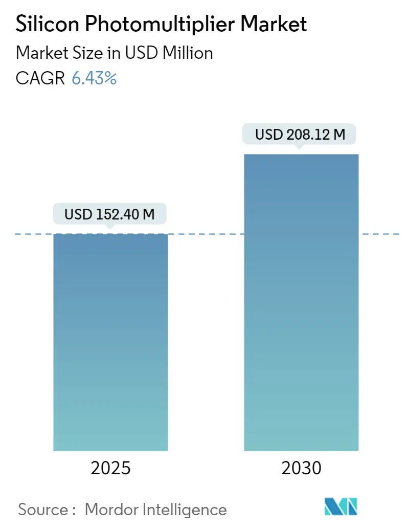
| Market Size (2025) | USD 152.40 Million |
| Market Size (2030) | USD 208.12 Million |
| Growth Rate (2025 - 2030) | 6.43% CAGR |
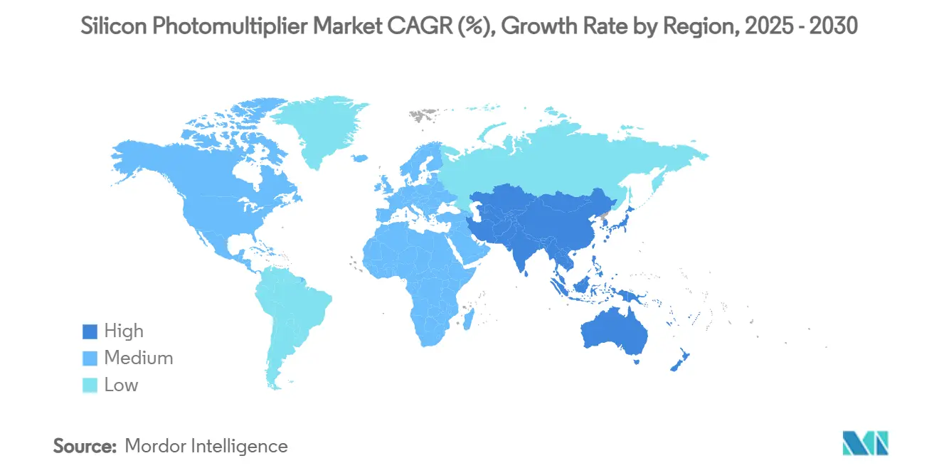
| Fastest Growing Market | Asia Pacific |
| Largest Market | North America |
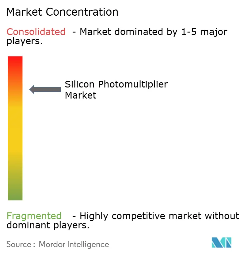
| Market Concentration | High |
Major Players *Disclaimer: Major Players sorted in no particular order Image © Mordor Intelligence. Reuse requires attribution under CC BY 4.0. | |
Silicon Photomultiplier Market Analysis by Mordor Intelligence
The silicon photomultiplier market size is USD 152.40 million in 2025 and is projected to reach USD 208.12 million by 2030, advancing at a 6.43% CAGR]. Demand accelerates as healthcare providers upgrade PET and SPECT scanners, automotive OEMs replace mechanical LiDAR detectors, and quantum research programs seek single-photon sensitivity in cryogenic conditions. Dominance of analog devices in 2024 reflects mature foundry processes, yet digital integration is closing the gap by simplifying read-out electronics and improving timing performance. North American incumbency comes from a dense cluster of medical-imaging OEMs, while Asia-Pacific growth stems from semiconductor investment and vehicle electrification roll-outs. Moderate competitive intensity lets technology leaders protect quench-resistor IP, but consolidation—Broadcom acquiring KETEK assets—signals an era of vertically integrated detector solutions.
Key Report Takeaways
- By application, medical imaging led with 45.60% revenue share in 2024, while LiDAR is forecast to expand at a 7.67% CAGR through 2030.
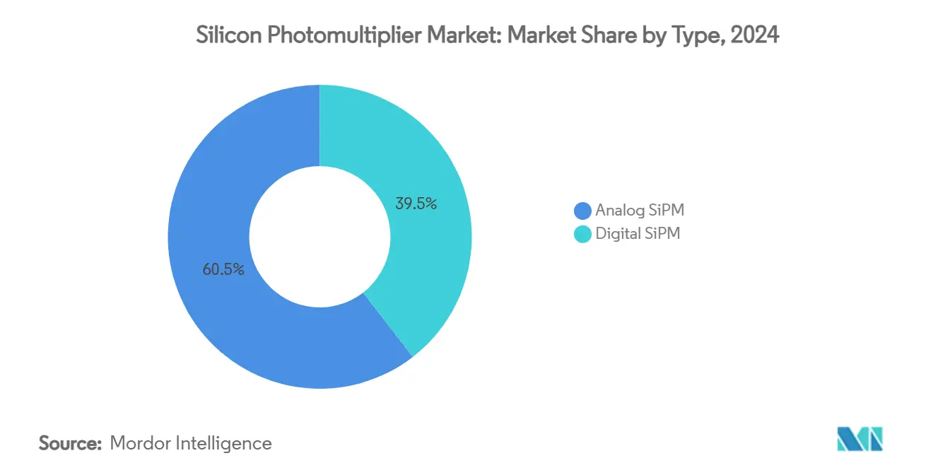
- By type, analog technology captured 60.50% of the silicon photomultiplier market share in 2024, whereas digital variants are projected to rise at an 8.02% CAGR to 2030.
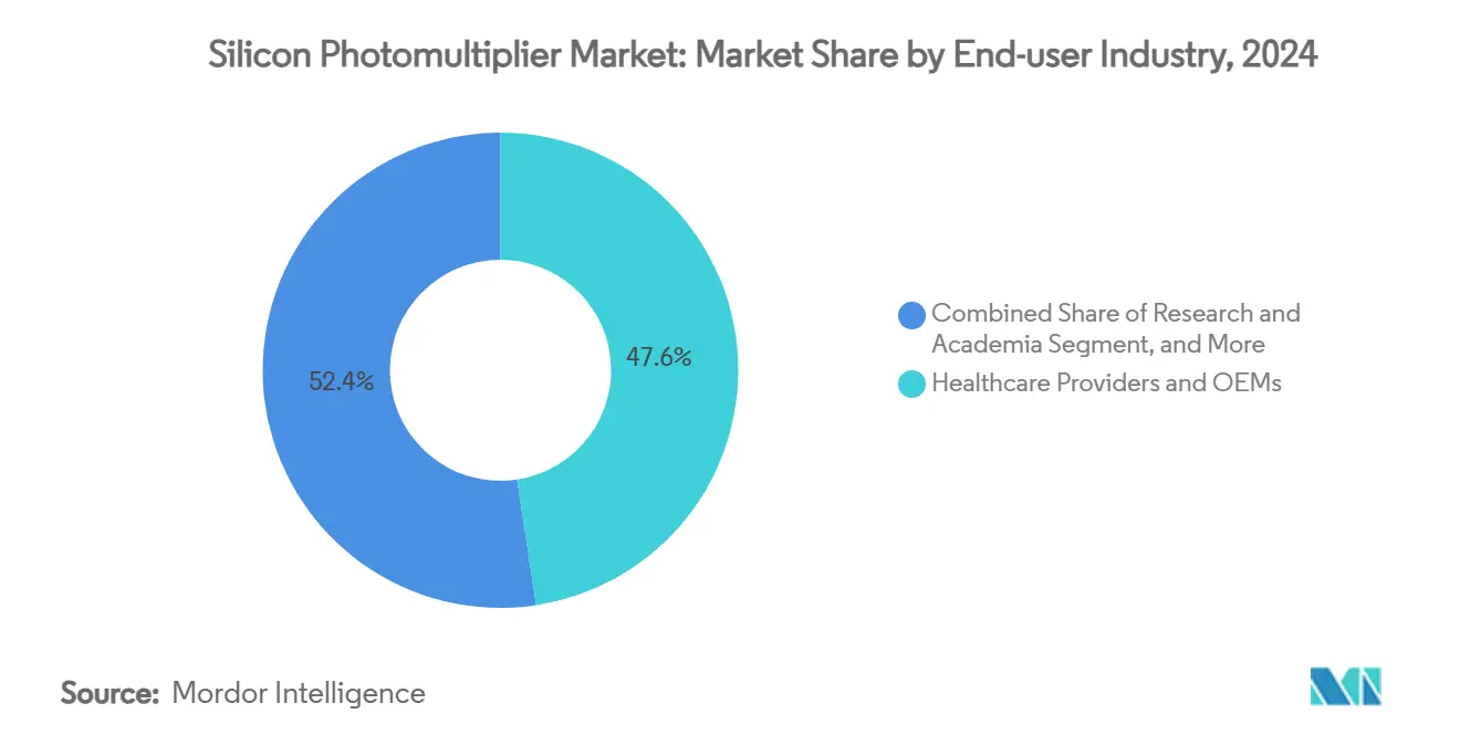
- By end-user industry, healthcare commanded 47.60% share of the silicon photomultiplier market size in 2024 and automotive is advancing at a 6.90% CAGR through 2030.
- By spectral range, near-UV devices held 43.60% revenue share in 2024, while NIR-optimized products will climb at a 7.12% CAGR up to 2030.
- By geography, North America accounted for 39.00% of total revenue in 2024; Asia-Pacific is tracking a 7.89% CAGR through 2030.
- Hamamatsu Photonics, onsemi, Broadcom, and Teledyne together controlled roughly 55% of 2024 revenues, underscoring a moderately concentrated landscape.
Global Silicon Photomultiplier Market Trends and Insights
Drivers Impact Analysis*
| Driver | (~) % Impact on CAGR Forecast | Geographic Relevance | Impact Timeline |
|---|---|---|---|
| PET/CT scan time-of-flight accuracy needs | +1.2% | Global; North America and Europe | Medium term (2–4 years) |
| Solid-state LiDAR adoption in autonomous vehicles | +1.8% | Global; Asia-Pacific and North America | Medium term (2–4 years) |
| Lower-voltage PMT-replacement advantages | +0.9% | Global | Long term (≥ 4 years) |
| Rising demand in flow-cytometry and biophotonics | +0.7% | North America and Europe | Short term (≤ 2 years) |
| Cryogenic m²-scale SiPM tiles for dark-matter physics | +0.4% | Europe and North America | Long term (≥ 4 years) |
| UV-enhanced SiPM enabling in-field UV–VIS spectroscopy | +0.3% | Global | Medium term (2–4 years) |
| Source: Mordor Intelligence | |||
PET/CT scan time-of-flight accuracy needs
Time-of-flight PET platforms require sub-200 ps resolution; silicon photomultipliers achieve 50 ps in optimized arrays, enabling radiation-dose reductions without sacrificing image quality.[1]Finn Feindt et al., “The DESY Digital Silicon Photomultiplier: Device Characteristics and First Test-Beam Results,” arxiv.org DarkSide-20k’s 21 m² deployment proves high-yield wafer production at 93.2%, supporting large medical detectors. Magnetic field immunity opens seamless PET-MRI integration, broadening multimodal imaging uptake. Compact die footprints let OEMs design portable PET scanners for bedside diagnostics. The result is a clear upgrade path away from vacuum photomultiplier tubes, accelerating replacement demand.
Solid-state LiDAR adoption in autonomous vehicles
Automotive LiDAR must record single photons from targets over 200 m with nanosecond precision; silicon photomultipliers deliver >10⁶ internal gain at <60 V bias, removing bulky high-voltage stages.[2]onsemi, “LiDAR Partners Program: Bringing the Ecosystem Together,” onsemi.com Stellantis Ventures’ funding of SteerLight validates OEM trust in solid-state architectures free of moving parts. Ambient-light immunity overcomes APD limitations in bright sunlight. Ecosystem programs, such as onsemi’s LiDAR Partners, shorten module qualification cycles. Cost curves point to price parity with mechanical LiDAR by 2027, mapping a route to high-volume adoption.
Lower-voltage PMT-replacement advantages
Photomultiplier tubes require 1,000-3,000 V supplies; silicon photomultipliers operate at 20-60 V, slashing power conversion complexity by 70% and enabling battery-driven instruments. Berkeley Nucleonics showed PET-grade performance from 12 V rails in 2024. Rugged solid-state construction resists vibration that can shatter glass envelopes in legacy detectors. Compatibility with standard CMOS masks leverages high-volume infrastructure, counteracting historical cost barriers. These factors collectively sustain long-run growth across industrial and field-portable platforms.
Rising demand in flow-cytometry and biophotonics
Flow cytometers sort 100,000 cells per second; silicon photomultipliers detect faint fluorescence from rare cell populations below 0.01% frequency, boosting clinical diagnostics. Broad UV-to-NIR response supports multi-color assays without channel-to-channel gain drift. Integrated on-chip digitization reduces baseline noise, widening the dynamic range in spectral cytometry. Falling device costs propagate adoption in resource-constrained labs. The uptick aligns with expanding cell-and-gene therapy pipelines that require detailed phenotyping.
Restraints Impact Analysis*
| Restraint | (~) % Impact on CAGR Forecast | Geographic Relevance | Impact Timeline |
|---|---|---|---|
| Optical crosstalk and after-pulsing noise | –1.1% | Global | Short term (≤ 2 years) |
| Cost premium vs. APDs in mass-volume OEM bids | –0.8% | Global; Asia-Pacific | Medium term (2–4 years) |
| Proprietary quench-resistor IP limiting multi-sourcing | –0.5% | Global | Long term (≥ 4 years) |
| Laser-safety regulation uncertainty (less than 920 nm LiDAR) | –0.3% | North America and Europe | Short term (≤ 2 years) |
| Source: Mordor Intelligence | |||
Optical crosstalk and after-pulsing noise
Avalanche events emit photons that retrigger adjacent pixels; rates span 2-40 %, eroding energy resolution and timing accuracy. After-pulses caused by trapped carriers release milliseconds later, introducing false counts in high-rate systems. Deep-trench isolation can suppress crosstalk below 5 % but adds 15-20 % to wafer cost. Operating at lower over-voltage mitigates noise yet reduces photon-detection efficiency. Active cooling stabilizes dark count rate, raising system complexity and power demand.
Cost premium vs. APDs in mass-volume OEM bids
Automotive LiDAR modules with 64-element arrays can cost USD 10,000 when built on silicon photomultipliers, compared to USD 2,000 for APD equivalents. Limited foundry capacity restrains economies-of-scale, cutting price declines to 20-30 % even at six-figure volumes. OEMs prefer dual sourcing; proprietary architectures restrict alternative supply. The resulting procurement risk favors cheaper APD sensors in cost-sensitive trims, delaying full conversion.
*Our forecasts treat driver/restraint impacts as directional, not additive. The impact forecasts reflect baseline growth, mix effects, and variable interactions.
Segment Analysis
By Type: Digital integration accelerates performance
Analog devices supplied 60.50% revenue in 2024 through proven CMOS flows and wide dynamic range, marking them the largest slice of the silicon photomultiplier market. Digital variants embed time-to-digital converters on die, trimming bill-of-materials and elevating 50 ps timing that underpins time-of-flight PET. The silicon photomultiplier market size for digital devices is forecast to rise at an 8.02% CAGR, overtaking analog share in high-precision niches by 2030. Hybrid architectures combining analog gain with digital read-out are emerging to balance cost and performance. Foundry specialization remains a hurdle, yet roadmap commitments from STMicroelectronics and LFoundry illustrate volume readiness.
Growing LiDAR interest forces device makers to enhance crosstalk mitigation without sacrificing efficiency. Vendors introduce trench isolation and separating guard-rings that relax over-voltage constraints. Concurrently, analog technology gains incremental improvements via lower dark count rates and shrinked pixel pitches, delaying digital’s outright dominance. The silicon photomultiplier industry thus shows a two-track evolution: mainstream analog upgrades for price-sensitive segments and premium digital offerings for timing-critical systems.


By Application: Medical imaging dominance faces LiDAR challenge
Medical imaging held 45.60% revenue share in 2024, securing the top position within the silicon photomultiplier market.[3]Diagnostics Journal, “Technological Advances in SPECT and SPECT/CT Imaging,” mdpi.com Hospitals upgrade PET detectors to exploit sub-200 ps timing for dose reduction and MRI compatibility. The silicon photomultiplier market size attached to scanning suites remains resilient as installed bases cycle every seven to ten years. LiDAR represents the fastest mover at 7.67% CAGR, fueled by autonomous-driving commitments from global automakers. Commercial pilots in robo-taxis and heavy trucks prove the reliability of solid-state architecture employing 905 nm arrays.
BioPhotonics, flow cytometry, and radiation monitoring occupy niche yet stable demand pools strengthened by a regulatory push for point-of-care diagnostics. High-energy physics continues as a technology incubator, with JUNO-TAO and DarkSide-20k validating meter-scale array assembly. Environmental sensing and industrial inspection are nascent but promising as unit economics improve. Collectively, application diversity cushions cyclicality in any single vertical.
By End-User Industry: Healthcare leadership under automotive pressure
Healthcare accounted for 47.60% of 2024 revenue, cementing a leading role across the silicon photomultiplier market share. PET-scanner retrofits and new MRI-compatible designs underpin predictable volume. Automotive and transportation post a 6.90% CAGR, pushed by ADAS feature mandates and collision-avoidance incentives. Manufacturers such as Tesla and Volvo plan multi-sensor configurations, expanding detector counts per car.
Industrial automation adopts SiPMs in laser-distance and surface-inspection tools demanded by precision manufacturing. Research institutions leverage grant funding for quantum sensing and astrophysics missions, adding irregular but sizable orders. Defense and aerospace entities validate long-term reliability in space, offering margin-rich contracts. Consumer electronics involvement remains exploratory, limited by cost constraints. This split illustrates how the silicon photomultiplier industry is diversifying beyond its medical roots.

By Spectral Range: Near-UV dominance shifts toward NIR growth
Near-UV/blue optimized devices secured 43.60% revenue in 2024 through synergy with LYSO/BGO scintillators prevalent in PET scanners. Optimization at 420 nm maximizes photon yield from crystal matrices. NIR-sensitive products are slated for a 7.12% CAGR to 2030, primarily due to 905 nm automotive LiDAR demand. The silicon photomultiplier market size for NIR devices scales with every percentage of vehicle penetration.
UV/VUV devices fill specialized research roles in xenon-based detectors and vacuum-UV spectroscopy. Visible-RGB products address general imaging, though APDs still dominate cost-sensitive CCTV and barcode readers. Increasing wafer-level coating precision allows vendors to tailor spectral response per vertical, supporting portfolio segmentation. Efforts to push 1,550 nm detection for fiber-optic links are under early study, hinting at longer-term diversification.
Geography Analysis
North America’s silicon photomultiplier market generated the largest regional revenue share at 39.00% in 2024. Uptake stems from hospital PET-upgrade programs, well-funded research centers and aerospace payloads seeking radiation-tolerant sensors. Local supply from onsemi and Hamamatsu subsidiaries simplifies prototyping, while NASA grants spur space-rated designs. Venture capital channels finance startups pursuing integrated photonic modules, reinforcing a pipeline of novel end-use cases. Export-control considerations increasingly favor domestic manufacturing, though wafer processing often still occurs in Japan.
Asia-Pacific is forecast for 7.89% CAGR, fastest worldwide, as silicon photomultiplier market penetration expands through China’s ADAS roll-outs and Korea’s consumer-electronics giants exploring 3-D sensing. Government incentives funnel billions into chip fabs, positioning the region for cost-optimized SiPM production. Japanese leadership continues via Hamamatsu’s R&D throughput, yet mainland initiatives aim to localize entire value chains. India’s growing healthcare infrastructure introduces new orders for PET-CT scanners, while Australian research hubs test VUV-sensitive arrays in dark-matter observatories. Political tensions over tech transfer shape partnership models but do not diminish underlying demand growth.
Europe ranks third in revenues but first in collaborative research intensity. CERN-linked programs drive meter-square array procurements, supporting suppliers in Italy and Germany. Germany’s automotive sector pursues solid-state LiDAR to comply with Euro NCAP roadmaps, bolstering regional shipments. France and the United Kingdom integrate SiPM payloads on small satellites, proving survivability in radiation belts. STMicroelectronics’ 2025 relaunch of silicon photonics production at Crolles indicates a strategic desire for regional semiconductor sovereignty. Eastern European nations participate through niche assembly services, rounding out a balanced regional ecosystem.

Competitive Landscape
Building-Automation/HVAC Retrofits in Mature Economies
The silicon photomultiplier market remains moderately concentrated. Hamamatsu Photonics combines a 90% photomultiplier tube share with a 203.9 billion yen turnover, leveraging installed-base relationships to cross-sell SiPM upgrades. onsemi capitalizes on a USD 7.08 billion revenue scale to invest in automotive qualification, though Q1 2025 sales softened as destocking persisted. Broadcom enhanced vertical capabilities via KETEK asset acquisition, adding sensor expertise to its optoelectronic switch roadmap.[4]Broadcom Inc., “Broadcom Delivers Industry's First 51.2-Tbps Co-Packaged Optics Ethernet Switch Platform,” investors.broadcom.com
Teledyne’s USD 710 million purchase of select Excelitas operations in 2024 brings integrated detector-camera assemblies into a unified offering. FBK and LFoundry focus on specialty wafer runs yielding >93 % for scientific arrays, underlining niche leadership where larger IDMs lack process flexibility. Patent portfolios on quench resistors, deep-trench isolation and digital multiplexing create barriers; however, IEEE standardization could eventually lower vendor lock-in. Start-ups targeting CMOS-compatible resistorless designs aim to trim cost curves and gain automotive Tier-1 approvals. M&A momentum suggests further consolidation as capital intensity rises.
White-space remains in price-sensitive consumer products where APDs dominate. Vendors are testing 1-inch wafer panelization and backside-illuminated variants to boost die counts per substrate, thereby reducing unit cost. Digital-on-analog hybrids promise entry-level pricing with incremental functionality. Sustainability narratives underline lower operating voltages and extended MTBF compared to glass tubes, supporting green-procurement criteria. Ultimately, execution on cost roadmaps will decide share shifts as automotive volumes dwarf legacy medical demand.
Silicon Photomultiplier Industry Leaders
Hamamatsu Photonics K.K.
ON Semiconductor Corporation
Broadcom Inc.
Excelitas Technologies Corp.
KETEK GmbH Halbleiter
- *Disclaimer: Major Players sorted in no particular order

Recent Industry Developments
- July 2025: ZEISS acquired all shares of Pi Imaging Technology SA to integrate SPAD and SiPM expertise into life-science microscopes.
- February 2025: STMicroelectronics restarted silicon photonics mass production at Crolles, reinforcing European supply chains.
- February 2025: onsemi announced FY 2024 revenue of USD 7.08 billion, reaffirming focus on intelligent sensing portfolios including SiPM.
- January 2025: Broadcom introduced a 51.2-Tbps co-packaged optics switch that exploits internal silicon photonics, aligning with SiPM detector needs for assembly testing.


Global Silicon Photomultiplier Market Report Scope
| Analog SiPM |
| Digital SiPM |
| Medical Imaging (PET, SPECT, PET-CT, PET-MRI) |
| LiDAR (Automotive, Industrial) |
| BioPhotonics and Flow Cytometry |
| High-Energy and Astro-Particle Physics |
| Nuclear and Radiation Monitoring |
| Environmental / Industrial Sensing |
| Other Applications |
| Healthcare Providers and OEMs |
| Automotive and Transportation |
| Industrial and Manufacturing Automation |
| Research and Academia |
| Defense and Aerospace |
| Other End-user Industries |
| UV/VUV (200-350 nm) |
| Near-UV / Blue (350-480 nm) |
| RGB / Visible (480-700 nm) |
| NIR (700-950 nm) |
| North America |
| South America |
| Europe |
| Asia Pacific |
| Middle East and Africa |
| By Type | Analog SiPM |
| Digital SiPM | |
| By Application | Medical Imaging (PET, SPECT, PET-CT, PET-MRI) |
| LiDAR (Automotive, Industrial) | |
| BioPhotonics and Flow Cytometry | |
| High-Energy and Astro-Particle Physics | |
| Nuclear and Radiation Monitoring | |
| Environmental / Industrial Sensing | |
| Other Applications | |
| By End-user Industry | Healthcare Providers and OEMs |
| Automotive and Transportation | |
| Industrial and Manufacturing Automation | |
| Research and Academia | |
| Defense and Aerospace | |
| Other End-user Industries | |
| By Spectral Range | UV/VUV (200-350 nm) |
| Near-UV / Blue (350-480 nm) | |
| RGB / Visible (480-700 nm) | |
| NIR (700-950 nm) | |
| By Geography | North America |
| South America | |
| Europe | |
| Asia Pacific | |
| Middle East and Africa |


Key Questions Answered in the Report
What is the current size of the silicon photomultiplier market?
The silicon photomultiplier market size is USD 152.40 million in 2025.
What CAGR is forecast for the global silicon photomultiplier market to 2030?
The market is projected to grow at a 6.43% CAGR between 2025 and 2030.
Which application currently dominates silicon photomultiplier demand?
Medical imaging, particularly PET and SPECT scanners, held 45.60% revenue share in 2024.
Which region is expected to grow fastest in silicon photomultiplier adoption?
Asia-Pacific is forecast to exhibit a 7.89% CAGR through 2030 due to semiconductor and automotive investment.
Who are the leading companies in the silicon photomultiplier space?
Key players include Hamamatsu Photonics, onsemi, Broadcom and Teledyne, together controlling about 55% of market revenue.
What is the main technical advantage of silicon photomultipliers over photomultiplier tubes?
They deliver single-photon sensitivity at low bias voltages (20-60 V) while remaining immune to magnetic fields, enabling compact and rugged sensor designs.
Page last updated on:


