Silicon On Insulator Market Size and Share
Market Overview
| Study Period | 2020 - 2031 |
|---|---|
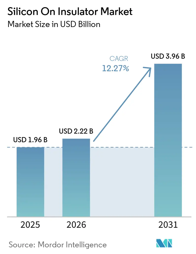
| Market Size (2026) | USD 2.22 Billion |
| Market Size (2031) | USD 3.96 Billion |
| Growth Rate (2026 - 2031) | 12.27% CAGR |
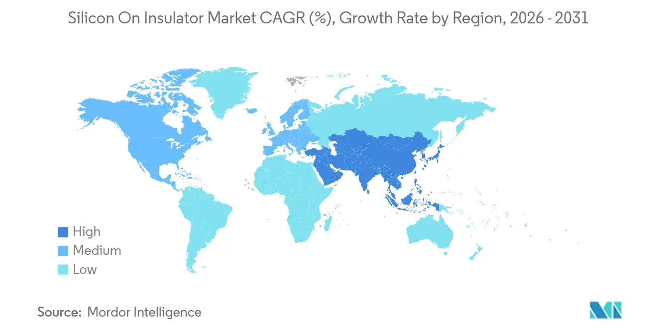
| Fastest Growing Market | Middle East |
| Largest Market | Asia Pacific |
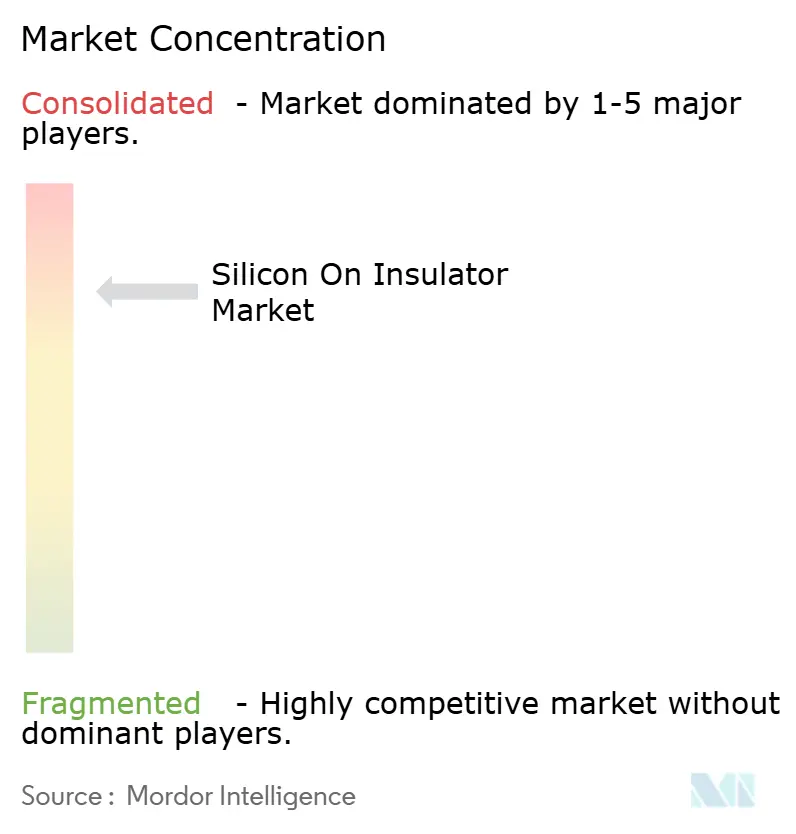
| Market Concentration | High |
Major Players *Disclaimer: Major Players sorted in no particular order Image © Mordor Intelligence. Reuse requires attribution under CC BY 4.0. | |
Silicon On Insulator Market Analysis by Mordor Intelligence
The silicon-on-insulator market size was valued at USD 1.96 billion in 2025 and is estimated to grow from USD 2.22 billion in 2026 to USD 3.96 billion by 2031, at a CAGR of 12.27% during the forecast period (2026-2031). Subsidies embedded in the United States CHIPS and Science Act, the European Chips Act, and China’s National Integrated Circuit Industry Investment Fund are steering demand toward domestic SOI wafer ecosystems, particularly for fully depleted and power variants that outperform bulk CMOS in leakage control and breakdown voltage. Momentum is also coming from 5G millimeter-wave radios, edge AI accelerators, and 800 V electric-vehicle inverters, each of which favors SOI’s buried-oxide isolation. Foundries that have qualified 22 nm and 12 nm FD-SOI platforms can now co-integrate analog, digital, and power blocks on a single die, reducing bill-of-materials costs while meeting emerging performance specifications. Meanwhile, lingering shortages of 300 mm SOI substrates underscore the strategic importance of the capacity expansions announced by front-runners in the wafer supply chain.
Key Report Takeaways
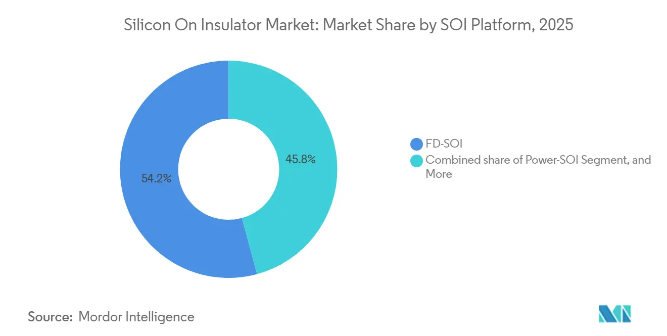
- By the SOI platform, fully depleted silicon-on-insulator led with a 54.21% revenue share in 2025, while power-SOI is projected to advance at a 13.07% CAGR through 2031.
- By wafer size, substrates measuring 201 mm or more accounted for 68.33% of demand in 2025, and the ≥201 mm category is forecast to grow at a 12.67% CAGR to 2031 as Smart Cut capacity ramps at new 300 mm fabs.
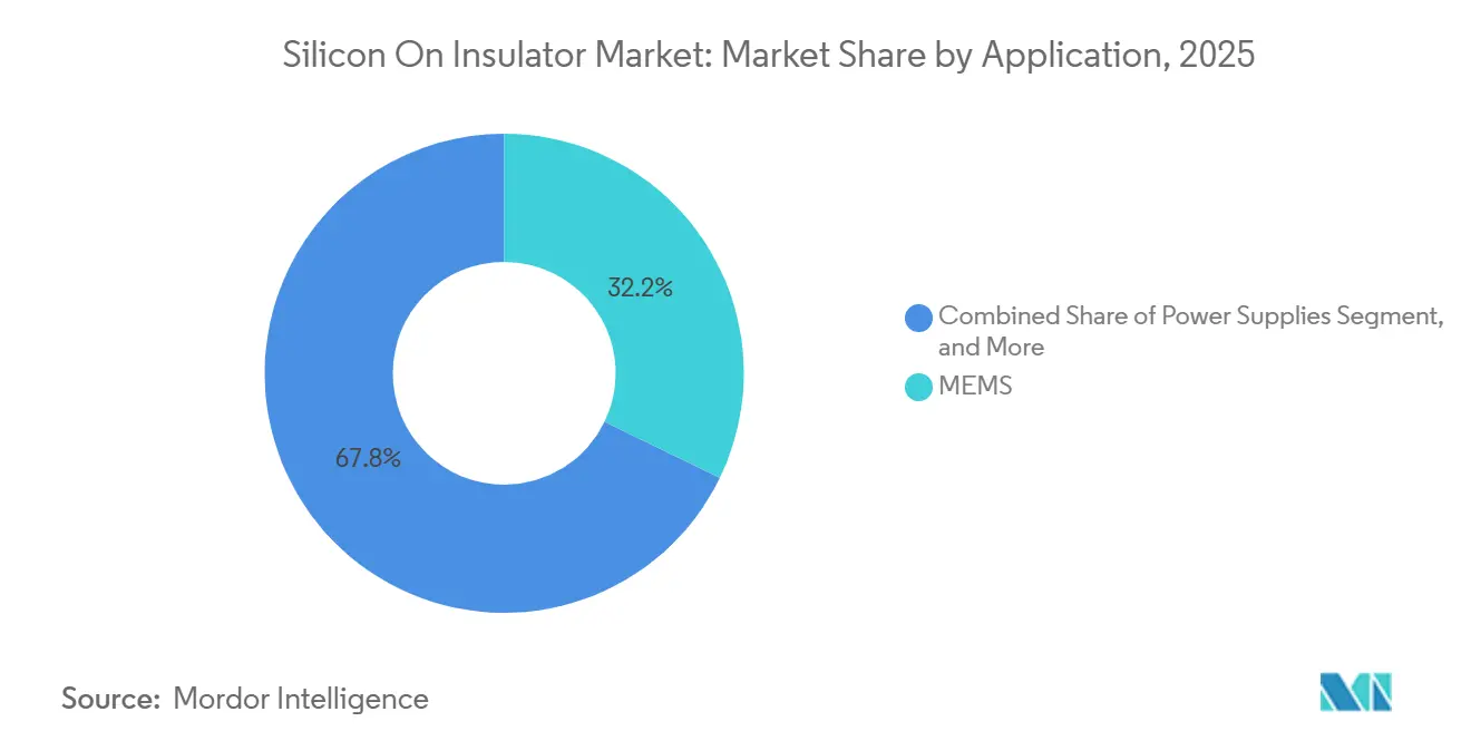
- By application, MEMS captured 32.18% share in 2025 thanks to pervasive use in smartphones, wearables, and industrial automation, and the optical communication is expected to expand at a 13.27% CAGR to 2031.
- By end-user vertical, consumer electronics accounted for 41.43% of the market in 2025, and the automotive industry is on track for a 13.47% CAGR through 2031 as electrification and advanced driver-assistance systems multiply SOI content per vehicle.
- By geography, Asia-Pacific held 46.83% of global revenue in 2025, driven by China’s indigenous foundry build-out, and the Middle East is set for the fastest growth, with a 13.21% CAGR through 2031.
Note: Market size and forecast figures in this report are generated using Mordor Intelligence’s proprietary estimation framework, updated with the latest available data and insights as of January 2026.
Global Silicon On Insulator Market Trends and Insights
Driver Impact Analysis*
| Driver | (~) % Impact on CAGR Forecast | Geographic Relevance | Impact Timeline |
|---|---|---|---|
| Expanding Adoption of FD-SOI in 5G RF Front-End Modules | +2.8% | Global, concentrated in North America, Europe and Asia-Pacific | Medium term (2-4 years) |
| Growing Demand for High-Performance, Low-Power Edge AI Chips | +2.5% | Global, led by North America and Asia-Pacific | Medium term (2-4 years) |
| Governments' Strategic Semiconductor Sovereignty Initiatives | +2.3% | North America, Europe and Asia-Pacific | Long term (≥4 years) |
| Electric-Vehicle Powertrain Efficiency Improvements Using Power-SOI | +2.1% | Global, early adoption in Europe, North America and China | Medium term (2-4 years) |
| Rising Use of MEMS Sensors in Industry 4.0 Applications | +1.2% | Asia-Pacific core, spillover to Europe and North America | Short term (≤2 years) |
| Surge in Optical Interconnects for Data Centers Leveraging SOI Photonics | +1.4% | North America and Asia-Pacific, expanding to Middle East | Medium term (2-4 years) |
| Source: Mordor Intelligence | |||
Expanding Adoption of FD-SOI in 5G RF Front-End Modules
Smartphone radio architectures integrate more power amplifiers, switches, and tuners to support carrier aggregation, with FD-SOI providing required linearity and harmonic suppression without costlier substrates. RF-SOI wafer shipments grew significantly in 2025 as multi-band flagships launched. Foundries now produce 22 nm FD-SOI nodes for radio applications, combining analog, digital, and power blocks on a single die to reduce PCB footprints. 3GPP Release 18 standards, met by FD-SOI through real-time back-biasing, further drive wafer demand, boosting the silicon-on-insulator market. FD-SOI is also being adopted for massive-MIMO radios, expanding growth beyond handsets.
Growing Demand for High-Performance, Low-Power Edge AI Chips
Edge inference engines in vehicles, cameras, and wearables must meet milliwatt standby budgets while delivering tera-operations-per-second performance. FD-SOI’s ultra-thin body reduces leakage and supports operation down to 0.4 V, driving automotive AI SoCs to adopt 28 nm FD-SOI platforms in 2025. Engineers use back-bias to manage temperature swings from -40 °C to 125 °C, meeting safety mandates without adding guard-band voltage. Standardizing this approach increases wafer volume, lowers costs, and boosts adoption, expanding the silicon-on-insulator market.
Governments' Strategic Semiconductor Sovereignty Initiatives
Over USD 100 billion in public funding is directed toward domestic fabs to address supply-chain risks, with allocations for FD-SOI and power semiconductor lines. The European Chips Act dedicates EUR 43 billion (USD 48.4 billion) to double Europe’s semiconductor output by 2030, with pilot lines in France and Germany focused on SOI specialty nodes.[1]European Commission, “Chips Act Fact Sheet,” EC.EUROPA.EU The U.S. CHIPS and Science Act offers tax incentives for 300 mm FD-SOI expansions in New York and Arizona. Subsidy structures require trusted-supplier guarantees, which encourage long-term contracts and stabilize market capacity. Export-control compliance drives buyers to source domestically or from allies, boosting regional demand.
Electric-Vehicle Powertrain Efficiency Improvements Using Power-SOI
Power-SOI substrates integrate gate drivers, current sensors, and protection logic on a single die, reducing parasitic inductance and switching losses in traction inverters. Automotive reference designs in 2025 showed 15% lower total-loss figures than discrete IGBT line-ups, adding 5% extra driving range per charge. With buried-oxide layers handling voltages over 1,200 V, Power-SOI supports 800 V battery architectures without a thicker bulk die. ISO 26262 qualification pipelines and mandates phasing out internal-combustion engines in key regions drive double-digit growth in this market.
Restraint Impact Analysis*
| Restraint | (~) % Impact on CAGR Forecast | Geographic Relevance | Impact Timeline |
|---|---|---|---|
| Supply-Demand Imbalance in 300 mm SOI Wafer Capacity | -1.8% | Global, acute in Asia-Pacific and North America | Short term (≤2 years) |
| High Fabrication Cost Versus Bulk Silicon Alternatives | -1.5% | Global | Long term (≥4 years) |
| Complexity of Integrating SOI With Advanced Packaging Technologies | -0.9% | Global, concentrated in automotive and HPC | Medium term (2-4 years) |
| IP Ownership and Licensing Barriers in Smart Cut Process | -0.7% | Global | Long term (≥4 years) |
| Source: Mordor Intelligence | |||
Supply-Demand Imbalance in 300 mm SOI Wafer Capacity
By 2025, only one high-volume 300 mm line reached scale, with expansions delayed until late 2027. Foundries face wafer costs 20%-30% higher than those for bulk silicon, squeezing margins and slowing migration to larger diameters. Some fabless customers shifted to 200 mm nodes to secure supply, but this diluted volumes and delayed cost curves, limiting near-term SOI market growth. Bulk-silicon giants remain cautious about SOI capex due to tighter thickness control and the higher capital intensity required for 300 mm hydrogen-implantation steps.[2]Shin-Etsu Chemical, “300 mm SOI Roadmap,” SHINETSU.CO.JP Short-term dual-sourcing remedies raise engineering overhead, providing only partial relief.
High Fabrication Cost Versus Bulk Silicon Alternatives
Layer-transfer and buried-oxide formation steps raise substrate costs by 30%-50%, requiring foundry utilization above 80% to sustain margins. While 22 nm FD-SOI nodes offer leakage and voltage-scaling benefits, some handset suppliers revert to bulk CMOS and use dynamic voltage-frequency scaling. The price gap narrows at 300 mm, but capacity shortages keep prices high, slowing adoption in cost-sensitive silicon-on-insulator segments. Automotive and RF designs benefit from reliability and power headroom, but price convergence depends on capacity expansions.
*Our forecasts treat driver/restraint impacts as directional, not additive. The impact forecasts reflect baseline growth, mix effects, and variable interactions.
Segment Analysis
By SOI Platform: FD-SOI Leads, Power-SOI Accelerates
The 54.21% revenue share held by FD-SOI in 2025 was the largest slice of the silicon-on-insulator market, buoyed by widespread deployment in RF transceivers, low-power microcontrollers, and consumer wearables. OEMs selected the platform for its ability to operate below 0.5 V while still delivering the gain linearity and noise margins demanded by next-generation radios. The silicon-on-insulator market size for Power-SOI is projected to grow at a 13.07% CAGR between 2026 and
At the process-technology level, GlobalFoundries’ 22 nm FD-SOI node recorded more than 50 automotive tape-outs by year-end 2025, confirming robust design-win momentum. STMicroelectronics and Samsung Foundry continue to proliferate FD-SOI across analog and mixed-signal catalogs, whereas Infineon and ON Semiconductor channel R&D toward Power-SOI for 800 V drive trains. This platform bifurcation enables wafer suppliers to fine-tune box and handle layers for application-specific needs, deepening value capture across the silicon-on-insulator industry.


By Wafer Size: ≥201 mm Maintains Dominance
Substrates measuring 201 mm or more captured 68.33% of 2025 revenue, reflecting die-per-wafer leverage that cuts costs by roughly one-third once volume reaches steady state. Most foundries are positioning 300 mm SOI lines in Europe and North America under government-backed subsidy programs, further anchoring this segment of the silicon-on-insulator market. However, Smart Cut at 300 mm demands sub-nanometer thickness uniformity; yield excursions therefore ripple quickly across hundreds of dies, underscoring the strategic importance of announced capacity increases.
Smaller diameters retain vitality in MEMS microphones, gyro sensors, and integrated photonics, where die footprints cap out far below a full reticle. Okmetic and Wafer Works maintain profitable niches in 150 mm and 200 mm runs, using faster cycle times to iterate alongside start-ups. Such capacity provides a relief valve, as designers hedge against the tight supply of 300 mm blanks, preserving resilience across the broader silicon-on-insulator market.
By Technology: Smart Cut Retains Lead, Layer Transfer Climbs
Smart Cut held 47.92% of revenue in 2025 and remains the technique of record for high-volume FD-SOI and RF-SOI applications that demand ±5 nm buried-oxide precision. Partial patent expirations have opened the way for alternative engineering approaches, yet decades of tacit know-how embedded in hydrogen-implant processes remain barriers. Layer-transfer methods that pair direct wafer bonding with chemical-mechanical polishing are advancing at a 12.87% CAGR, driven by cost-sensitive power devices in which oxide thickness tolerances are looser.
Bonding-SOI continues to play a critical role in serving the aerospace and radiation-hardened niches, even though the production volumes remain relatively modest. The competitive landscape in this domain has shifted focus from solely transistor geometry to more advanced heterogeneous-integration constructs, such as chip-on-wafer-on-substrate. These constructs still depend heavily on the planarity and thermal compatibility that the Smart Cut technology facilitates. This reliance underscores the importance of Smart Cut in maintaining innovation cycles and driving advancements across the silicon-on-insulator industry.
By Application: MEMS Retains Leadership, Optical Communication Surges
MEMS sensors accounted for 32.18% of revenue in 2025, solidifying their position as the cornerstone of market volume. The buried-oxide layer plays a crucial role by isolating capacitive structures, which enhances sensitivity in pressure and inertial sensing applications while maintaining a compact die size. This technological advantage has driven significant design wins, particularly for six-axis IMUs (Inertial Measurement Units) used in stability control systems and industrial robotics. These advancements have driven consistent growth in unit shipments, underscoring the importance of MEMS sensors across applications.
Optical communication is registering the fastest climb, with a 13.27% CAGR projected through 2031 as hyperscale operators standardize on 400 Gbps and 800 Gbps photonic transceivers. Intel alone shipped over 10 million SOI-based photonic modules by late 2025, elevating wafer demand linked to co-packaged optics. Power supplies, image sensing, and emerging categories such as quantum processors round out the balance, but their combined clip is still secondary to the momentum in photonics and MEMS in the silicon-on-insulator market.
By End-User Vertical: Consumer Electronics Dominates, Automotive Accelerates
Consumer electronics accounted for 41.43% of 2025 revenue, driven by the widespread adoption of FD-SOI switch arrays and envelope trackers in devices such as smartphones, tablets, and wearables. These components are increasingly integrated into consumer devices to support advanced functionalities, including improved connectivity and energy efficiency. While high production volumes have kept average selling prices competitive, the growing complexity of devices has increased the number of dies per device. This trend is particularly evident with the addition of new 5G bands and battery-life optimization features, which continue to sustain demand for wafers.
Automotive recorded the highest growth trajectory, expanding at a 13.47% CAGR to 2031 as battery-electric platforms and advanced driver-assistance systems mandate low-leakage, high-temperature ICs. Each electric vehicle now incorporates 3,000-5,000 chips, and a growing number leverage SOI substrates for robust isolation against ambient swings. Industrial, IT and telecommunications, and aerospace and defense make up the residual, with the latter paying premium prices for radiation-tolerant variants, thereby sustaining niche profitability within the silicon-on-insulator market.
Geography Analysis
Asia-Pacific commanded 46.83% of global revenue in 2025, anchored by China’s indigenous foundry surge and Japan’s enduring edge in precision MEMS fabrication. Taiwan and South Korea add depth through leading-edge logic and memory, while India’s Production-Linked Incentive scheme is drawing assembly and test investments that will back-propagate wafer demand.[3]Government of India, “Semiconductor PLI Scheme,” INDIA.GOV.IN Regional build-outs in 5G base stations and edge AI gateways further multiply consumption of FD-SOI and Power-SOI substrates.
North America combines sovereign-funded fab projects with long-standing aerospace and defense applications that value SOI for radiation hardness. Intel, GlobalFoundries, and TSMC have each broken ground on U.S. facilities slated to consume 300-mm specialty wafers when ramping begins in 2027. Europe follows closely, supported by EUR 43 billion (USD 48.4 billion) in Chips Act incentives that target automotive and industrial semiconductors. STMicroelectronics, Infineon, and NXP are already integrating localized SOI capacity into their roadmap to de-risk supply.
The Middle East represents the most dynamic frontier, with sovereign wealth funds allocating multibillion-dollar capital pools to semiconductor fabs focused on optical interconnects and AI accelerators. Pilot lines in the United Arab Emirates and Saudi Arabia plan to leverage SOI photonics to lower data-center energy intensity, reinforcing a 13.21% CAGR outlook for the region. South America and Africa are early in ecosystem development; nonetheless, pilot programs in Brazil and South Africa signal future upside for the silicon on insulator market as policy frameworks mature.

Competitive Landscape
The silicon-on-insulator market is dominated by Soitec, Shin-Etsu Chemical, and GlobalWafers for blank wafers, while GlobalFoundries, STMicroelectronics, and Samsung Foundry lead specialty process development. Vertical integration is increasing as substrate vendors and foundries co-optimize key parameters, raising switching costs. Although expiring Smart Cut patents lower entry barriers, tacit expertise for commercial yields remains a challenge for new entrants.
Chinese players, supported by the National Integrated Circuit Industry Investment Fund, are scaling domestic 200 mm and 300 mm SOI lines for SMIC and regional fabless clients, but yields still lag behind incumbents. Established suppliers focus on supply-chain security and joint development agreements to maintain market share and cushion price erosion. Patent filings with the World Intellectual Property Organization in 2025 indicate a shift toward system-level performance through heterogeneous integration.[4]World Intellectual Property Organization, “SOI Patent Filings 2025,” WIPO.INT
Opportunity white spaces span Power-SOI modules for 800 V EV inverters, SOI photonics for co-packaged optics, and radiation-tolerant substrates for small-satellite constellations. Incumbents have only partly invested here, inviting specialized start-ups to carve profitable niches. The landscape is expected to bifurcate into a high-margin, reliability-driven tier and a high-volume consumer tier, each demanding distinct cost-and-performance trade-offs, yet collectively sustaining growth in the silicon-on-insulator market.
Silicon On Insulator Industry Leaders
Shin-Etsu Chemical Co., Ltd.
GlobalWafers Co., Ltd.
STMicroelectronics N.V.
Soitec SA
GlobalFoundries Inc.
- *Disclaimer: Major Players sorted in no particular order

Recent Industry Developments
- March 2026: Soitec announced a EUR 500 million (USD 563 million) expansion of its 300 mm SOI facility in Bernin, France, aiming to lift annual capacity by 40% for automotive and RF supply.
- February 2026: NXP Semiconductors received ISO 26262 ASIL-D certification for its S32G network processor manufactured on a 16 nm FD-SOI line, validating functional-safety compliance.
- January 2026: GlobalFoundries and STMicroelectronics formed a USD 5.7 billion joint-venture fab in Crolles, France, dedicated to 18 nm and 12 nm FD-SOI processes for automotive and industrial chips.
- November 2025: Intel confirmed shipments of over 10 million SOI-based photonic transceivers for data-center optical links and outlined additional capacity in New Mexico.


Global Silicon On Insulator Market Report Scope
The Silicon on Insulator (SOI) market comprises the development, manufacturing, and commercialization of semiconductor wafers and devices built using silicon-on-insulator substrate technology, in which a thin silicon layer is separated from the bulk substrate by an insulating layer, typically silicon dioxide. SOI technology enhances device performance by reducing parasitic capacitance, lowering power consumption, improving switching speed, and enabling superior thermal and radiation tolerance compared to conventional bulk silicon architectures. These characteristics support broad adoption across advanced semiconductor applications, including RF front-end modules, MEMS devices, power electronics, photonics, automotive systems, and low-power computing platforms.
The Silicon on Insulator Market Report is Segmented by SOI Platform (FD-SOI, PD-SOI, Power-SOI, and Other SOI Platforms), Wafer Size (≤200 mm, and ≥201 mm), Technology (Bonding SOI, Layer Transfer SOI, and Smart Cut), Application (MEMS, Power Supplies, Optical Communication, Image Sensing, and Other Applications), End-User Vertical (Consumer Electronics, Automotive, IT and Telecommunication, Aerospace and Defense, Industrial, and Other End-User Verticals), and Geography (North America, South America, Europe, Asia-Pacific, and Middle East and Africa). The Market Forecasts are Provided in Terms of Value (USD).
| Fully Depleted Silicon on Insulator (FD-SOI) |
| Partially Depleted Silicon on Insulator (PD-SOI) |
| Power-SOI |
| Other Types |
| Less Than or Equal To 200 mm |
| 201 mm and Above |
| Bonding SOI |
| Layer Transfer SOI |
| Smart Cut |
| MEMS |
| Power Supplies |
| Optical Communication |
| Image Sensing |
| Other Applications |
| Consumer Electronics |
| Automotive |
| IT and Telecommunication |
| Aerospace and Defense |
| Industrial |
| Other End User Verticals |
| North America | United States | |
| Canada | ||
| Mexico | ||
| South America | Brazil | |
| Argentina | ||
| Rest of South America | ||
| Europe | United Kingdom | |
| Germany | ||
| France | ||
| Italy | ||
| Rest of Europe | ||
| Asia-Pacific | China | |
| Japan | ||
| India | ||
| South Korea | ||
| Rest of Asia-Pacific | ||
| Middle East and Africa | Middle East | United Arab Emirates |
| Saudi Arabia | ||
| Rest of Middle East | ||
| Africa | South Africa | |
| Egypt | ||
| Rest of Africa | ||
| By SOI Platform | Fully Depleted Silicon on Insulator (FD-SOI) | ||
| Partially Depleted Silicon on Insulator (PD-SOI) | |||
| Power-SOI | |||
| Other Types | |||
| By Wafer Size | Less Than or Equal To 200 mm | ||
| 201 mm and Above | |||
| By Technology | Bonding SOI | ||
| Layer Transfer SOI | |||
| Smart Cut | |||
| By Application | MEMS | ||
| Power Supplies | |||
| Optical Communication | |||
| Image Sensing | |||
| Other Applications | |||
| By End-User Vertical | Consumer Electronics | ||
| Automotive | |||
| IT and Telecommunication | |||
| Aerospace and Defense | |||
| Industrial | |||
| Other End User Verticals | |||
| By Geography | North America | United States | |
| Canada | |||
| Mexico | |||
| South America | Brazil | ||
| Argentina | |||
| Rest of South America | |||
| Europe | United Kingdom | ||
| Germany | |||
| France | |||
| Italy | |||
| Rest of Europe | |||
| Asia-Pacific | China | ||
| Japan | |||
| India | |||
| South Korea | |||
| Rest of Asia-Pacific | |||
| Middle East and Africa | Middle East | United Arab Emirates | |
| Saudi Arabia | |||
| Rest of Middle East | |||
| Africa | South Africa | ||
| Egypt | |||
| Rest of Africa | |||


Key Questions Answered in the Report
What is the current size of the silicon on insulator market and how fast is it growing?
The silicon on insulator market size reached USD 2.22 billion in 2026 and is projected to climb to USD 3.96 billion by 2031, advancing at a 12.27% CAGR over 2026-2031.
Which SOI platform is most widely adopted today?
Fully depleted SOI leads, accounting for 54.21% of 2025 revenue thanks to its strong uptake in RF front-end modules and low-power edge AI chips.
Why is Power-SOI gaining traction in electric vehicles?
Power-SOI substrates integrate gate drivers and sensing circuits on one die, lower switching losses by up to 15% and handle voltages beyond 1,200 V, making them ideal for 800 V EV inverters.
How will the CHIPS and European Chips Acts influence regional SOI demand?
Both laws attach sizeable subsidies to on-shore specialty nodes, prompting new 300 mm FD-SOI fabs in the United States and Europe and thereby lifting local wafer demand.
What is the key supply constraint facing the silicon on insulator market?
A shortage of high-yield 300 mm SOI substrates persists, with additional capacity not expected to fully relieve tightness until late 2027.
Which application is forecast to grow fastest through 2031?
Optical communication, particularly SOI-based silicon photonics for 400 Gbps and 800 Gbps data-center links, is projected to expand at a 13.27% CAGR.
Page last updated on:


