Silicon Photonics Market Size and Share
Market Overview
| Study Period | 2020 - 2031 |
|---|---|
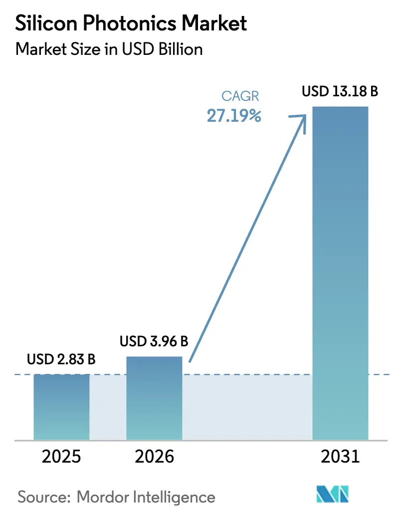
| Market Size (2026) | USD 3.96 Billion |
| Market Size (2031) | USD 13.18 Billion |
| Growth Rate (2026 - 2031) | 27.19% CAGR |
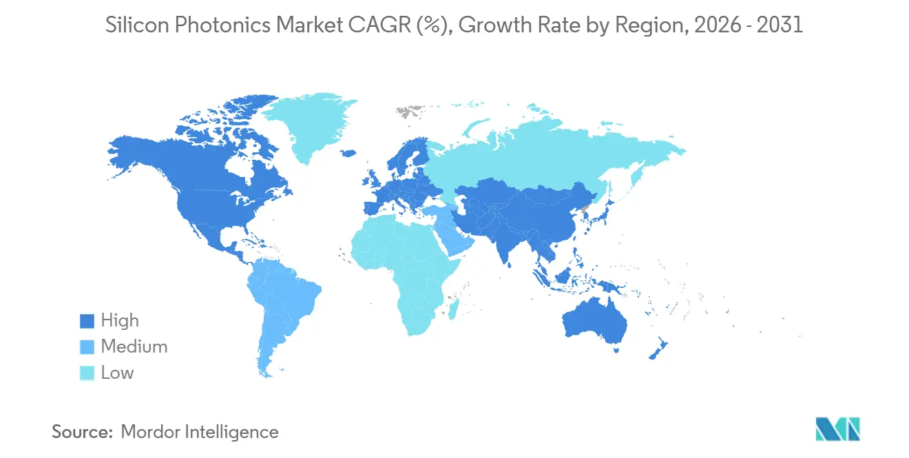
| Fastest Growing Market | Asia Pacific |
| Largest Market | North America |
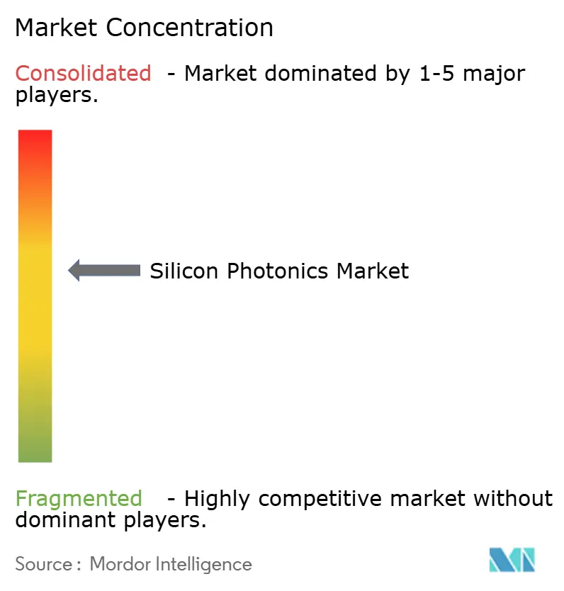
| Market Concentration | Medium |
Major Players *Disclaimer: Major Players sorted in no particular order Image © Mordor Intelligence. Reuse requires attribution under CC BY 4.0. | |
Silicon Photonics Market Analysis by Mordor Intelligence
The silicon photonics market size is projected to expand from USD 2.83 billion in 2025 and USD 3.96 billion in 2026 to USD 13.18 billion by 2031, registering a CAGR of 27.19% between 2026 to 2031. Strong capital outlays by hyperscale cloud operators, the transition from pluggable optics to co-packaged devices, and government incentives for domestic semiconductor capacity are accelerating adoption. Hyperscalers are replacing power-hungry copper links with optical lanes rated at 400 Gbps and 800 Gbps to keep GPU clusters within tight latency budgets. Co-packaged optics lower electrical trace lengths, cutting switch power draw by about 30% and helping data center operators hit aggressive carbon-reduction targets. At the same time, 300 mm photonics wafer capacity is expanding under CHIPS Act awards, although a near-term supply gap persists. The market outlook also hinges on progress in heterogeneous laser integration, where the direct bonding of III-V materials to silicon is expected to further shrink the cost per bit.
Key Report Takeaways
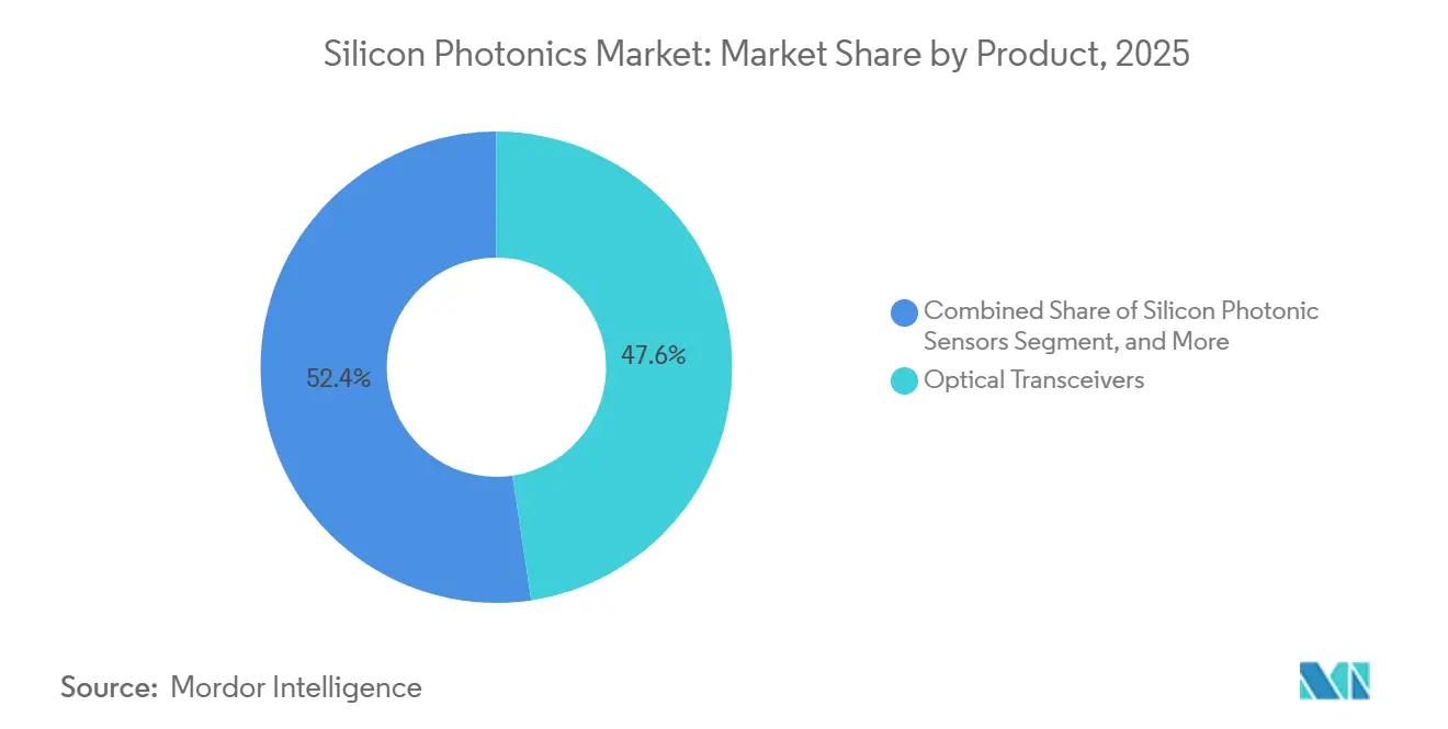
- By product, optical transceivers accounted for 47.64% of the silicon photonics market share in 2025, while silicon photonic sensors are projected to expand at a 28.74% CAGR through 2031.
- By component, active devices captured a 58.91% share in 2025 and are expected to grow at a 27.56% CAGR during the forecast window.
- By wafer size, 300 mm substrates commanded 62.33% of the silicon photonics market share in 2025, and this node is forecast to grow at a 27.73% CAGR through 2031.
- By data rate, 400 Gbps modules led with 53.64% share in 2025, whereas lanes above 1.6 Tbps are slated to record a 28.17% CAGR through 2031.
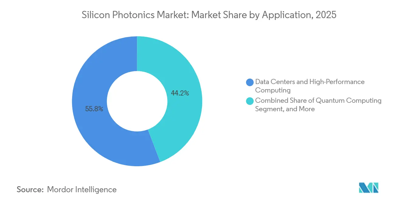
- By application, data centers and high-performance computing accounted for 55.78% of the silicon photonics market share in 2025, while quantum computing use is set to rise at a 28.79% CAGR over the same period.
- By end user, hyperscale cloud providers accounted for 58.72% of the silicon photonics market share in 2025, whereas automotive OEMs and Tier-1 suppliers are poised for a 28.34% CAGR through 2031.
- By geography, North America dominated with a 42.76% share in 2025, while the Asia-Pacific is projected to post the fastest 28.11% CAGR through 2031.
Note: Market size and forecast figures in this report are generated using Mordor Intelligence’s proprietary estimation framework, updated with the latest available data and insights as of January 2026.
Global Silicon Photonics Market Trends and Insights
Drivers Impact Analysis*
| Driver | (~) % Impact on CAGR Forecast | Geographic Relevance | Impact Timeline |
|---|---|---|---|
| Energy-efficient co-packaged optics adoption | +5.8% | North America and Asia-Pacific, spillover to Europe | Medium term (2-4 years) |
| Carbon-reduction mandates | +4.2% | Global, led by EU and California | Long term (≥ 4 years) |
| 5G fronthaul/backhaul upgrade | +3.9% | Asia-Pacific core, North America and Europe | Short term (≤ 2 years) |
| Automotive Level-3 LiDAR programs | +3.5% | North America and Europe, China EV market | Medium term (2-4 years) |
| Defense funding for quantum photonics | +2.7% | North America, select European agencies | Long term (≥ 4 years) |
| Government semiconductor incentives | +4.1% | North America, European Union, China | Medium term (2-4 years) |
| Source: Mordor Intelligence | |||
Energy-Efficient Co-Packaged Optics Adoption in Hyperscale Data Centers
Photonic dies are now bonded to switch silicon, removing the thermal penalties of pluggable optics and freeing valuable faceplate real estate. Marvell’s 51.2 Tbps platform employs micro-ring modulators delivering 200 Gbps per lane, lowering switch power by roughly 30%.[1]Investor Relations, “Marvell Announces Co-Packaged Optics Solution,” marvell.com NVIDIA and TSMC use advanced interposers to route optical signals among GPU chiplets, overcoming the electrical bandwidth ceiling at 224 Gbps. Fabrinet expanded its optical module capacity by USD 132.5 million to meet swelling demand for co-packaged optics. Although the Optical Internetworking Forum released draft guidance, each hyperscaler continues to pursue proprietary form factors, fragmenting supply and complicating vendor qualification.
Carbon-Reduction Mandates Driving Low-Power Optical Interconnects
Global regulators are tightening power-use limits amid data centers' 460 TWh consumption in 2024. Silicon photonics reduces interconnect energy consumption, enabling denser racks and higher inlet temperatures. The International Energy Agency warns electricity demand could double by 2030 without optical upgrades.[2]International Energy Agency, “Data Centers and Energy Demand,” iea.org Omdia forecasts USD 545 billion in AI-centric capital outlays by 2030, much of it channeled to energy-efficient links. Although photonic chip fabrication is energy-intensive, lifecycle analyses still favor optics over copper for hyperscale deployments.
5G Fronthaul/Backhaul Upgrade Fueling 400 G and 800 G Modules
Operators are rolling out 400G and 800G optics to meet low-latency fronthaul thresholds. Lumentum’s ZR+ line complies with ITU-T G.698.4 and targets metro spans exceeding 500 km.[3]Lumentum Holdings, “ZR+ Coherent Module Launch,” lumentum.com AT&T and Ciena validated 1.6 Tbps silicon photonics DSPs over existing fiber, demonstrating a path to multi-terabit backbones. Ericsson is embedding co-packaged optics inside radio units to cut weight and ease tower installation. Capital intensity remains a barrier in emerging markets, yet urban densification pushes carriers toward photonic links.
Automotive Level-3 LiDAR Programs Leveraging FMCW Silicon Photonics
OEMs are shifting from time-of-flight to FMCW sensors that integrate lasers, modulators, and detectors on a single die for sub-USD 500 targets. Aurora secured USD 1.7 billion to industrialize long-range FMCW LiDAR for autonomous trucking. General Motors allocated a share of its USD 1.3 billion Cruise budget to photonic-sensing R&D. Luminar booked USD 14.8 million in sales in Q3 2024, but yields and reliability still trail automotive norms. SAE J3016 Level-3 guidelines require redundant sensing, positioning silicon photonics as a core enabler.
Restraints Impact Analysis*
| Restraint | (~) % Impact on CAGR Forecast | Geographic Relevance | Impact Timeline |
|---|---|---|---|
| Thermal budget limits above 70 °C | -2.1% | Global, affects data center and automotive use | Short term (≤ 2 years) |
| Lack of standardized packaging | -1.8% | Global, acute in North America and Europe | Medium term (2-4 years) |
| Competition from InP and polymer photonics | -1.3% | Global, focused on long-haul telecom and sensing | Long term (≥ 4 years) |
| Limited 300 mm photonic foundry capacity | -2.5% | Global, most severe in Asia-Pacific and North America | Short term (≤ 2 years) |
| Source: Mordor Intelligence | |||
Thermal Budget Limitations in Silicon Substrates Above 70 °C
Ring resonators drift 0.1 nm per °C, forcing closed-loop heaters and raising module power. Automotive ambient temperatures often exceed 85 °C, demanding costly cooling or derating. Data centers mitigate with liquid loops, yet added infrastructure inflates TCO. Researchers are exploring silicon carbide and aluminum nitride substrates to potentially reduce thermo-optic coefficients, yet widespread commercial adoption is still years off.
Lack of Standardized Packaging Elevating NRE Costs
Proprietary co-packaged optics pinouts and thermal constraints lock vendors into single-customer designs. OIF efforts are ongoing, but consensus on mechanical and thermal interfaces is not expected before 2027. Custom tooling drives per-design costs above USD 5 million, dampening startup participation and slowing multi-sourcing. Contract manufacturers cannot amortize equipment, so their unit economics lag those of well-established pluggable modules.
*Our forecasts treat driver/restraint impacts as directional, not additive. The impact forecasts reflect baseline growth, mix effects, and variable interactions.
Segment Analysis
By Product: Transceivers Dominate, Sensors Accelerate
Transceivers accounted for the largest share of the silicon photonics market, holding 47.64% in 2025, propelled by hyperscale adoption of 400 G and 800 G optics. Sensors, while smaller, will post the fastest 28.74% CAGR thanks to FMCW LiDAR and refractive index biosensing. Many switch vendors are eyeing on-board lasers, suggesting some standalone transceiver volumes may migrate onto ASIC packages. Active optical cables cater to AI clusters that cannot tolerate the bulk of copper, while optical switches remain hampered by control-plane complexity.
The rise of biosensing and automotive applications signals diversification beyond telecom. Aurora’s FMCW LiDAR showcases centimeter-level accuracy at 300 m range, a feat that relies on wafer-scale silicon photonics integration. In pharma, resonant-shift sensors speed high-throughput assays without fluorescent dyes, opening new licensing revenue for chip suppliers. DARPA’s PIPES program is funding all-optical packet switching, suggesting optical routers could eventually disrupt electrical fabrics.


By Component: Active Devices Lead Integration Push
Active devices accounted for 58.91% of the silicon photonics market share in 2025 and are projected to expand at a 27.56% CAGR. Lasers remain the costliest part because silicon’s indirect bandgap necessitates bonded III-V gain layers. Recent lab work demonstrated quantum-dot lasers monolithically grown on silicon, a leap that could slash the bill of materials once commercialized. Modulator bandwidth has climbed to 200 Gbps per lane using PAM4, enabling upcoming 1.6 Tbps pluggables.
Passive components, while essential, are witnessing a slower growth trajectory. Their yield is contingent on waveguide roughness and alignment tolerances, where even a single defect can jeopardize die performance. Proposals by OIF to standardize grating-coupler specifications could potentially reduce iteration cycles. With GPU vendors increasingly adopting co-packaged optics, the laser attachment process is transitioning from module houses to OSAT providers, effectively reshaping the supply chain landscape.
By Wafer Size: 300 mm Scales Economics
The 300 mm category accounted for 62.33% of the silicon photonics market in 2025 and will grow at a 27.73% CAGR. Larger wafers increase die output per lot, driving down cost and aligning photonics with mainstream CMOS depreciation schedules. GlobalFoundries and Intel secured a combined USD 10 billion in CHIPS Act grants to install 300 mm photonics tooling in U.S. fabs. Even so, McKinsey predicts a 40-60% shortfall in transceivers through 2027 as demand outstrips capacity.
Grating-coupler lithography and germanium epitaxy, distinct from logic flows, complicate the migration from 200 mm foundries. This transition requires significant adjustments in manufacturing processes and equipment, adding to the complexity. While Tower Semiconductor operates 200 mm lines, its clients increasingly advocate for a shift to 300 mm to achieve lower die costs and improved scalability. At 300 mm, TSMC’s CoWoS integrates photonics chiplets, facilitating heterogeneous stacking alongside logic and HBM memory, which enhances performance and efficiency in advanced applications.

By Data Rate: 400 G Dominates, 1.6 T Emerges
Modules rated at 400 Gbps held 53.64% share in 2025, making them the primary bandwidth currency inside hyperscale fabrics. Above-1.6 Tbps pluggables should soar at 28.17% CAGR, fueled by 51.2 Tbps switch ASICs that require 64×800 G or 32×1.6 T lanes. AT&T, in collaboration with Ciena's silicon-based DSP, successfully validated a transmission rate of 1.6 Tbps per wavelength over standard fiber, paving the way for imminent commercial rollouts.
As operators phase out 10 G and 25 G lanes, the once-dominant 100 G traffic sees a decline, signaling a shift in network infrastructure strategies. Meanwhile, the 200 G standard emerges as a cost-sensitive link for established brownfield networks, offering a transitional solution before higher-capacity standards are widely adopted. In a significant move, IEEE 802.3 working groups have not only solidified the 800 G standard but have also laid the groundwork for 1.6 T Ethernet clauses, dispelling any doubts about interoperability and paving the way for next-generation network advancements.
By Application: Data Centers Lead, Quantum Computing Emerges
Data centers and HPC retained a 55.78% share in 2025, anchored by AI training clusters hungry for near-chip bandwidth. Quantum computing applications, while niche, are forecast to expand at a blistering 28.79% CAGR. Researchers from the University of Bristol showcased entanglement on a single-piece silicon photonics chip, highlighting its potential for widespread quantum logic applications. This achievement demonstrates the feasibility of using silicon photonics as a scalable platform for quantum computing, paving the way for advancements in quantum technologies.
Telecommunications continues to invest in coherent optics for metro and long-haul links. Automotive LiDAR enters volume ramps starting 2026 as OEMs ship Level-3 systems. Healthcare firms use label-free photonics sensors in clinical diagnostics, though FDA pathways lengthen commercialization timelines. Defense agencies sponsor secure photonic communications, with quantum key distribution pilots moving from lab to field.
By End User: Hyperscalers Dominate, Automotive Accelerates
Hyperscale cloud providers accounted for 58.72% of the market in 2025, reflecting the continual expansion of multi-rack GPU complexes. Alphabet spent USD 17.2 billion on capex in Q1 2025, with photonic interconnects accounting for the bulk of the spend. As FMCW LiDAR becomes a standard feature on premium electric vehicles, automotive OEMs and Tier-1 suppliers are poised to experience a robust growth rate of 28.34% CAGR.
Telecom carriers face capex pressures yet must upgrade fronthaul to 400 G and beyond to support densified radios. Medical device companies are exploring in vivo photonic probes for high-resolution imaging. Government and defense entities prioritize sovereign photonics supply amid rising geopolitical risks. Universities continue to incubate early-stage IP, feeding the startup pipeline through technology-transfer agreements.
Geography Analysis
North America held a 42.76% share in 2025, buoyed by CHIPS Act funding and vertically integrated giants such as Intel, Cisco, and Broadcom. Local access to hyperscale customers enables fast co-design cycles, while DARPA grants spur photonic packet-switching R&D. While high labor costs and lengthy permitting processes can delay fab builds, fiscal incentives significantly alleviate this burden by reducing the financial strain on companies. These incentives often include tax breaks, grants, and subsidies, which help offset the challenges associated with high operational expenses and regulatory delays.
Asia-Pacific will post the quickest 28.11% CAGR through 2031. TSMC’s advanced packaging nodes enable chiplets containing photonics, logic, and memory to coexist on a single substrate, reducing interconnect power consumption. China’s Made in China 2025 plan allocates billions to fab construction, aiming to localize supply and mitigate export-control risk. Japan’s optics expertise and Korea’s 5G rollouts also underpin demand. Geopolitical frictions, however, threaten cross-border equipment flows and IP licensing.
Europe benefits from the EUR 43 billion EU Chips Act, yet fragmentation across member states impedes scale. Germany’s Fraunhofer institutes lead automotive LiDAR integration, while France’s CEA-Leti partners with foundries to build pilot lines. Automotive carbon mandates and data-sovereignty rules create pull for energy-efficient photonics, although higher energy and labor costs erode manufacturing competitiveness. The Middle East and Africa, plus South America, remain early adopters, chiefly in telecom backbones upgrading to 400 G.

Competitive Landscape
Consolidation is moderate, with the five largest vendors controlling about 60% of global transceiver revenue. Intel leverages a vertically integrated business model that spans photonics design, wafer fabrication, advanced packaging, and system assembly. Cisco has acquired several photonics startups since 2023, allowing it to bundle optical modules with its switching hardware for enterprise and service-provider customers. Broadcom focuses on custom silicon for hyperscalers, offering switch ASICs that integrate photonic interfaces tailored to Meta and Google data-center architectures.
Fabless players such as Marvell and Juniper Networks rely on foundry partners, including GlobalFoundries and Tower Semiconductor, trading capital efficiency for less control over manufacturing schedules. Marvell introduced a 51.2 Tbps co-packaged optics platform in January 2025, claiming a 30% reduction in switch power usage compared with pluggable modules. Juniper is sampling an optical I/O chiplet aimed at AI accelerators that require sub-5 ns latency across sockets. Ayar Labs, a venture-backed startup, has begun low-volume shipments of optical chiplets that support 32 channels at 112 Gbps each, targeting memory disaggregation use cases. PsiQuantum is working with GlobalFoundries to fabricate photonic qubit arrays, positioning the company for future revenue in quantum computing infrastructure.
Supply risk persists because only a handful of foundries can run 300 mm photonics processes at scale, and any political or natural-disaster disruption could choke capacity. GlobalFoundries and Intel both secured CHIPS Act grants in 2024 to expand domestic photonics fabs, but additional capacity will not come online until late 2026. Indium-phosphide vendors still dominate long-haul links, yet their share is limited to spans beyond 1.55 µm, where silicon is less efficient. The Optical Internetworking Forum is drafting a common co-packaged optics specification that could lower non-recurring engineering costs and open the market to a broader supplier base.
Silicon Photonics Industry Leaders
Intel Corporation
Cisco Systems Inc.
Lumentum Holdings Inc.
Juniper Networks Inc.
Sicoya GmbH
- *Disclaimer: Major Players sorted in no particular order

Recent Industry Developments
- April 2025: Alphabet announced Q1 2025 results showing USD 17.2 billion in capital expenditures, with substantial investment directed to co-packaged optics and 400 G/800 G transceivers.
- March 2025: Hyperscale cloud providers collectively committed USD 17.2 billion in capital outlays for the quarter, earmarking a large share for co-packaged optics that place photonic dies alongside switch ASICs.
- February 2025: NVIDIA released its fiscal 2025 annual report, citing USD 115.2 billion in data-center revenue fueled by demand for 400 Gbps and 800 Gbps optical transceivers.
- January 2025: Marvell Technology unveiled a 51.2 Tbps co-packaged optics platform featuring 200 Gbps-per-lane micro-ring modulators.


Research Methodology Framework and Report Scope
Market Definitions and Key Coverage
Our study treats the silicon photonics market as the total annual revenue generated from components and modules built on CMOS-compatible silicon or silicon-on-insulator wafers that integrate optical and electronic functions on the same die. Typical products include integrated transceivers, waveguides, modulators, photodetectors, and related assemblies supplied to data-center, telecom, automotive, and emerging quantum systems.
Scope exclusion: devices fabricated primarily in III-V materials, discrete passive optics, and foundry wafer services sold without packaged components are left outside this revenue pool.
Segmentation Overview
- By Product
- Optical Transceivers
- Optical Switches
- Active Optical Cables (AOCs)
- Silicon Photonic Sensors
- Wafer-Level Test Systems
- Multiplexers/De-Multiplexers
- Attenuators and Modulators
- Other Products
- By Component
- Active Components
- Lasers
- Modulators
- Photodetectors
- Passive Components
- Waveguides
- Filters
- Couplers
- Other Passive Components
- Active Components
- By Wafer Size
- 300 mm
- 200 mm
- 150 mm and Below
- By Data Rate
- Above 100 Gbps
- 200 Gbps
- 400 Gbps
- 800 Gbps
- Above 1.6 Tbps
- By Application
- Data Centers and High-Performance Computing
- Telecommunications
- Automotive and Autonomous Vehicles
- AR/VR and Consumer Electronics
- Healthcare and Life Sciences
- Defense and Aerospace
- Quantum Computing
- Other Applications
- By End-User
- Hyperscale Cloud Providers
- Telecom Operators
- Automotive OEMs and Tier-1 Suppliers
- Medical Device Manufacturers
- Government and Defense Agencies
- Research and Academic Institutions
- By Geography
- North America
- United States
- Canada
- Mexico
- Europe
- Germany
- United Kingdom
- France
- Italy
- Rest of Europe
- Asia-Pacific
- China
- Japan
- India
- South Korea
- Australia
- Rest of Asia-Pacific
- Middle East and Africa
- Middle East
- Saudi Arabia
- United Arab Emirates
- Rest of Middle East
- Africa
- South Africa
- Egypt
- Rest of Africa
- Middle East
- South America
- Brazil
- Argentina
- Rest of South America
- North America
Detailed Research Methodology and Data Validation
Primary Research
We then interview CMOS foundry engineers, optical transceiver product managers, hyperscale procurement leads, and telecom planners across North America, Europe, and Asia-Pacific. Their insights validate adoption timelines, price-roadmap inflections, and capacity utilization, helping us adjust preliminary desk estimates.
Desk Research
Mordor analysts begin with open data from bodies such as the U.S. Bureau of Industry & Security, SEMI, the Optical Internetworking Forum, and the National Science Foundation, which frame global wafer starts, transceiver shipments, and photonics R&D funding. Periodicals like IEEE Photonics Journal, European Photonics Industry Consortium briefs, and Data Center Dynamics add technology cadence and hyperscale build-out signals. Company 10-Ks, S-1 filings, and presentations hosted on D&B Hoovers and Dow Jones Factiva provide unit sales ranges and average selling prices that anchor our baseline. These references illustrate, not exhaust, the full secondary source set we examine.
Market-Sizing & Forecasting
Initial values are derived top-down by reconstructing global silicon photonics wafer output and die yields, then aligning those volumes with packaged-module penetration in data-center racks, 5G front-haul links, and automotive LiDAR builds. Select bottom-up checks, sampled vendor shipment roll-ups and channel ASP × volume triangulations, calibrate totals. Key variables fed into our multivariate regression forecast include hyperscale MW additions, quarterly 400 G/800 G transceiver shipments, 300 mm photonics wafer starts, 5G macro-cell counts, and ASP erosion curves. Where supplier disclosures lack granularity, proxy metrics (e.g. reticle exposure hours or import codes HS 851762) bridge gaps.
Data Validation & Update Cycle
Outputs pass a two-step analyst review: variance tests against independent indicators, followed by peer sign-off. Reports refresh every twelve months, with interim revisions if material events, fab expansions, export controls, and major design wins, shift the outlook. A final pre-publication sweep ensures clients receive our latest view.
Why Mordor's Silicon Photonics Baseline Commands Confidence
Published market values often diverge because firms choose dissimilar product mixes, price assumptions, and update cadences. According to Mordor Intelligence, anchoring on silicon-only integrated devices and annualizing both merchant and captive shipments yields a 2025 value of USD 3.11 billion, which we regard as the most decision-ready midpoint.
Benchmark comparison
| Market Size | Anonymized source | Primary gap driver |
|---|---|---|
| USD 3.11 B (2025) | Mordor Intelligence | - |
| USD 2.65 B (2025) | Regional Consultancy A | Excludes automotive & LiDAR demand and applies a conservative 400 G transition pace |
| USD 3.27 B (2025) | Global Consultancy B | Adds foundry service revenue and assumes aggressive ASP inflation dampening |
These comparisons show that scope breadth, ASP treatment, and refresh timing drive most discrepancies. By centering on verifiable silicon-based module revenue and overlaying continual primary checks, Mordor delivers a balanced, transparent baseline that stakeholders can trace back to clear variables and repeatable steps.


Key Questions Answered in the Report
What CAGR is forecast for the silicon photonics market from 2026 to 2031?
The market is projected to expand at a 27.19% CAGR over the period.
Which application generated the largest revenue in 2025?
Data centers and high-performance computing accounted for 55.78% of spending in 2025.
Why are hyperscale cloud providers investing in co-packaged optics?
Co-packaged optics cut switch power by roughly 30% and provide the bandwidth density required for multi-rack GPU clusters.
Which region is expected to grow fastest through 2031?
Asia Pacific is projected to post the highest CAGR at 28.11%, driven by advanced packaging and local supply-chain initiatives.
What is the main supply-side risk facing silicon photonics vendors?
Limited 300 mm photonics wafer capacity could create a 40-60% transceiver shortfall through 2027.
Page last updated on:


