Phototransistor Market Size and Share
Market Overview
| Study Period | 2019 - 2030 |
|---|---|
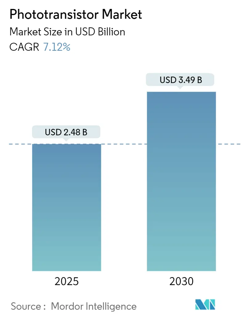
| Market Size (2025) | USD 2.48 Billion |
| Market Size (2030) | USD 3.49 Billion |
| Growth Rate (2025 - 2030) | 7.12% CAGR |
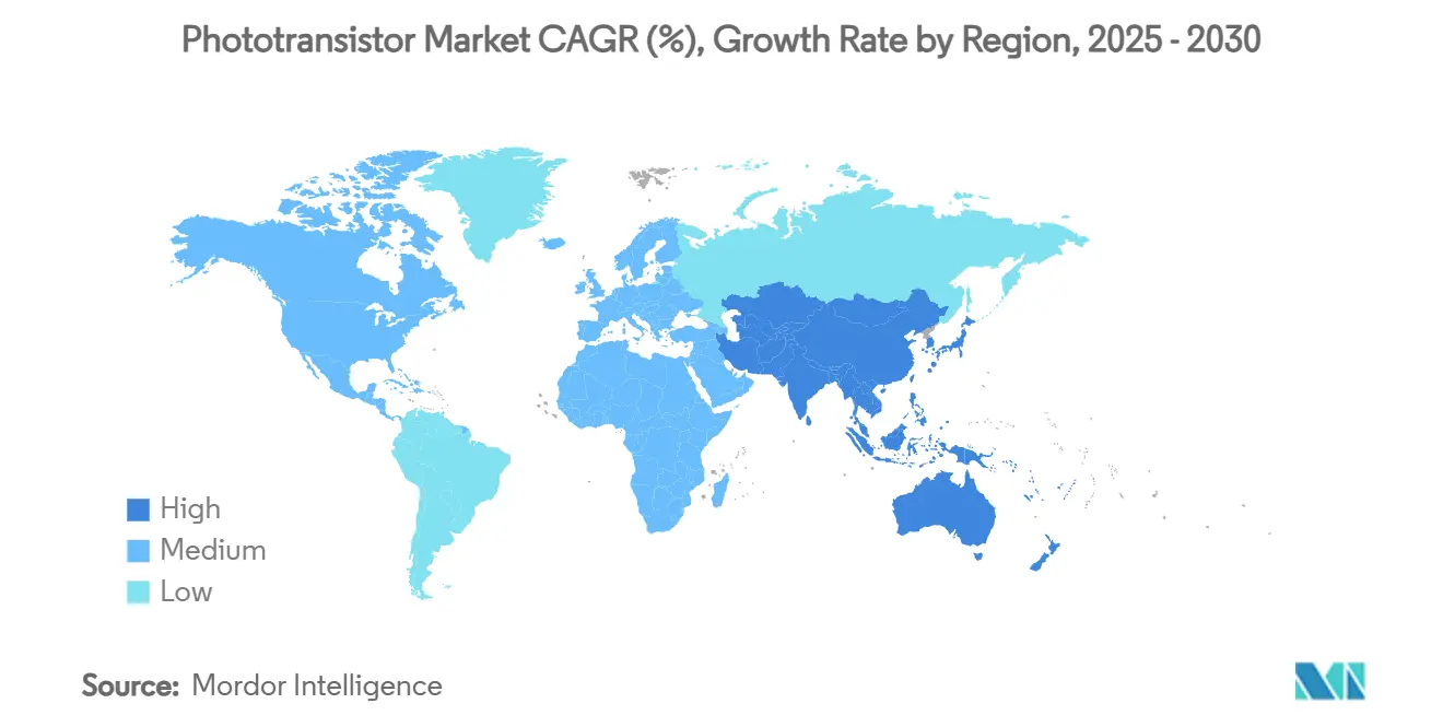
| Fastest Growing Market | Asia Pacific |
| Largest Market | North America |
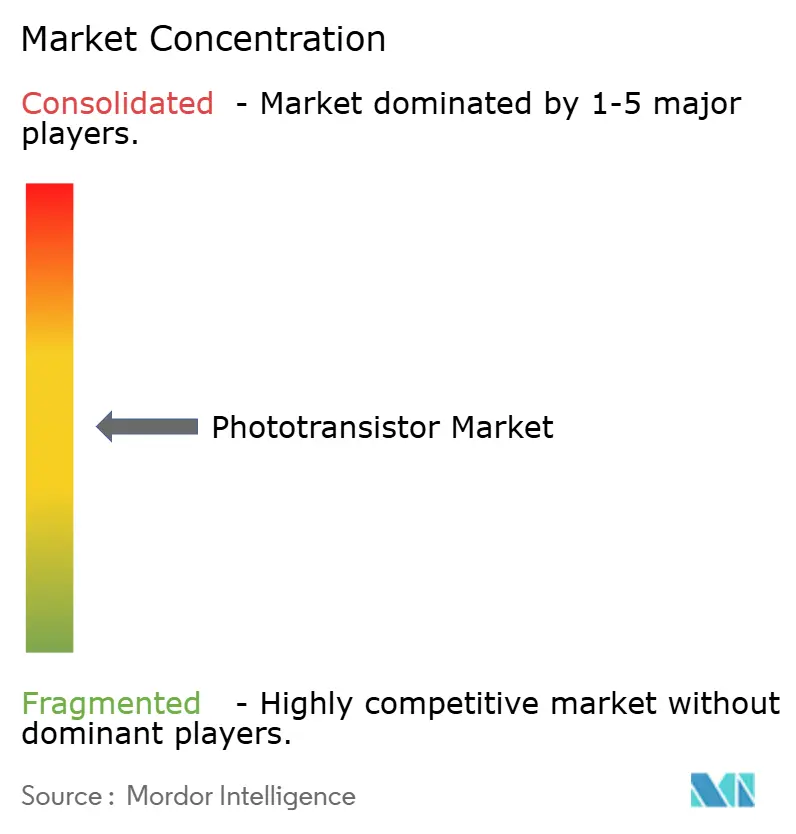
| Market Concentration | Medium |
Major Players *Disclaimer: Major Players sorted in no particular order Image © Mordor Intelligence. Reuse requires attribution under CC BY 4.0. | |
Phototransistor Market Analysis by Mordor Intelligence
The phototransistor market size stood at USD 2.48 billion in 2025 and is forecast to climb to USD 3.49 billion by 2030, translating to a 7.12% CAGR over the period. Expanding semiconductor capital investment, the surge of neuromorphic computing research, and widening deployment in consumer devices, cars, and smart factories underpin this trajectory. Silicon nanowire and perovskite quantum-dot innovations raise operating speeds toward the petahertz realm and widen the spectrum of detectable light, while government funding in the United States, Japan, and the European Union reduces regional supply risk.[1]“Researchers develop petahertz phototransistor,” Phys.org, phys.orgDemand also benefits from post-pandemic sterilization protocols that call for ultraviolet light monitoring, and from autonomous-vehicle LiDAR designs that require rapid optical isolation. However, recurring quartz-supply shocks and price volatility in wide-bandgap wafers expose the sector to cost swings. Despite these headwinds, sustained design wins in smartphones, medical imaging systems, and industrial Internet-of-Things (IoT) nodes signal healthy long-term growth for the phototransistor market.[2]onsemi, “Company press releases,” onsemi.com
Key Report Takeaways
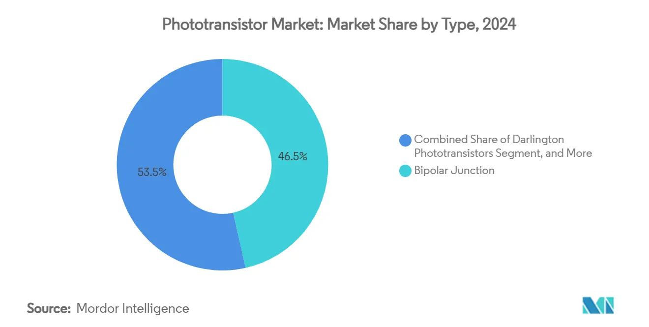
- By type, bipolar-junction led with 46.50% of phototransistor market share in 2024, whereas field-effect designs posted the highest 7.67% CAGR through 2030.
- By material, silicon accounted for 63.20% of the material mix in 2024 in the phototransistor market, while emerging compounds such as perovskites and metal oxides advanced at an 8.23% CAGR.
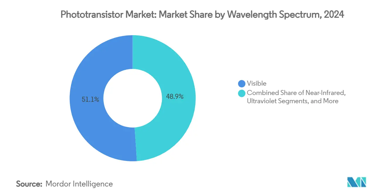
- By wavelength Spectrum, visible-spectrum products captured 51.08% of revenue in 2024 in the phototransistor market; ultraviolet variants are expanding at an 8.35% CAGR on sterilization and environmental-monitoring demand.
- By end-user industry, consumer electronics commanded 36.45% of revenue in 2024 in the phototransistor market; healthcare and life-sciences applications are accelerating at a 7.35% CAGR due to biosensing and diagnostic adoption.
- By geography, North America represented 39.00% of sales in 2024 in the phototransistor market ; Asia-Pacific is the fastest region with a 7.87% CAGR as Japan and Taiwan enlarge foundry capacity.
Global Phototransistor Market Trends and Insights
Drivers Impact Analysis*
| Driver | (~) % Impact on CAGR Forecast | Geographic Relevance | Impact Timeline |
|---|---|---|---|
| Smartphone sensor proliferation | +1.8% | Global with Asia-Pacific lead | Short term (≤ 2 years) |
| Automotive isolation via optocouplers | +1.5% | North America and Europe automotive corridors | Medium term (2–4 years) |
| Industrial automation and IoT light sensing | +1.3% | Asia-Pacific manufacturing hubs, spillover to MEA | Medium term (2–4 years) |
| Perovskite and oxide ultra-gain designs | +0.9% | Global R&D, early roll-out in North America | Long term (≥ 4 years) |
| Neuromorphic phototransistor arrays | +0.7% | North America and Europe research institutions | Long term (≥ 4 years) |
| RoHS-driven redesign cycles | +0.5% | EU with global supply-chain influence | Short term (≤ 2 years) |
| Source: Mordor Intelligence | |||
Smartphone sensor proliferation
Multiple-camera handsets now embed as many as five dedicated optical modules that manage depth mapping, ambient-light tuning, and computational photography. Each module specifies discrete gain and spectral windows that favor custom phototransistor architectures over photodiodes. Foldable and under-display designs tighten board space and push suppliers toward higher-gain, lower-noise components. Mid-tier smartphones adopt features once exclusive to flagships, enlarging annual unit consumption. Together these design shifts lift average phototransistor content per handset and support premium pricing for wavelength-selective parts.
Automotive isolation via optocouplers
Electric-vehicle battery packs, traction inverters, and 800 V fast-charging lines require strict signal isolation. Modern EVs integrate dozens of optocouplers to safeguard battery-management and motor-control circuits, expanding phototransistor content by roughly one order of magnitude versus combustion cars. LiDAR modules add further demand as phototransistors perform dual sensing and isolation duties. Compliance with ISO 26262 functional-safety mandates favors incumbents that can demonstrate automotive-grade reliability over extended temperature ranges.
Industrial automation and IoT light sensing
Smart factories deploy dense optical-sensor grids for color matching, surface inspection, and material identification. Optically powered sensor nodes cut electromagnetic interference in harsh shop-floor environments and reach power-transfer efficiencies near 24%.[3]“Optically Powered Wireless Sensor Nodes,” mdpi.com Edge processing embedded at the sensor trims latency and network bandwidth. In precision agriculture, multispectral phototransistor arrays track plant-stress indicators across red, green, and blue bands, enabling data-driven input management and yield gains.
Perovskite and oxide ultra-gain designs
Organolead-halide perovskites reach responsivity values above 2 × 10⁹ A/W and specific detectivity near 1.7 × 10¹⁴ Jones, outclassing bulk silicon by several orders of magnitude. Persistent photoconductivity enables optical memory effects vital for neuromorphic hardware because synaptic weights can be written optically without external memory. Transparent zinc-oxide and indium-oxide channels post field-effect mobility exceeding 40 cm²/V·s, opening pathways for display-integrated sensors. Encapsulation advances lessen moisture degradation and inch the materials toward mass production.
Restraints Impact Analysis*
| Restraint | (~) % Impact on CAGR Forecast | Geographic Relevance | Impact Timeline |
|---|---|---|---|
| CMOS image-sensor substitution | -1.2% | Global, strongest in consumer electronics | Short term (≤ 2 years) |
| Temperature-driven performance drift | -0.8% | Automotive and industrial deployments worldwide | Medium term (2–4 years) |
| SiC epitaxial-wafer price swings | -0.6% | Global supply chain concentrated in Asia-Pacific | Short term (≤ 2 years) |
| Optical side-channel security risk | -0.4% | High-security systems in North America and Europe | Long term (≥ 4 years) |
| Source: Mordor Intelligence | |||
CMOS image-sensor substitution
Stacked pixel architecture and hybrid bonding merge light capture and in-sensor signal processing, erasing the separate gain stage historically served by discrete phototransistors. Quantum efficiency approaches theoretical limits, and per-pixel analog memory adds dynamic range that competes head-on with discrete solutions. Cost pressures in smartphones and webcams accelerate the switch, though extreme-sensitivity or custom-spectral tasks still tip in favor of stand-alone phototransistors.
Temperature-driven performance drift
Phototransistor dark current rises roughly 1.15 µA per °C beyond 50 °C, cutting signal-to-noise ratios in engine compartments or steel mills. Wide-bandgap silicon-carbide options withstand up to 175 °C but carry higher die cost. Active temperature-compensation circuits inflate footprint and power draw, chipping at the core simplicity advantage of these devices.
*Our forecasts treat driver/restraint impacts as directional, not additive. The impact forecasts reflect baseline growth, mix effects, and variable interactions.
Segment Analysis
By Type: Field-effect architectures strengthen neuromorphic computing prospects
Field-effect devices registered the fastest 7.67% CAGR through 2030 as developers exploit gate bias to vary synaptic weight in optical neural networks. Bipolar-junction alternatives retained 46.50% of the phototransistor market share in 2024 thanks to decades of design-in across analog amplification roles.
Darlington pairs stay relevant in long-haul industrial links that demand amplified current over noisy cabling, while avalanche and heterojunction variants fill specialized telecom and aerospace slots. Momentum in quantum-switching research hints at future generations that harness tunneling effects to top current gain ceilings, positioning field-effect lines as the backbone of next-wave neuromorphic hardware.


By Material: Compound semiconductors challenge silicon hegemony
Silicon delivered 63.20% of revenue in 2024, safeguarding low-cost, high-yield production lines that underpin consumer, industrial, and medical volume programs. Emerging perovskite, oxide, and silicon-carbide blends are rising at an 8.23% CAGR due to higher responsivity, broader spectral reach, and elevated temperature resilience.
Germanium stays crucial for fiber-optic transceivers at 1.55 µm, while InGaAs shoots for even deeper infrared operation, albeit at premium die prices. Two-dimensional layers of graphene and transition-metal dichalcogenides unlock flexible or transparent form factors fit for wearable displays and bio-patches. As these alternatives mature, multi-stack wafers that marry silicon logic with compound-semiconductor phototransistors are likely to dominate the high-performance corner of the phototransistor market.
By Wavelength Spectrum: Ultraviolet uptake accelerates post-pandemic sterilization
Visible-range devices held a 51.08% revenue share in 2024 because consumer cameras, ambient-light adjusters, and display dimmers adopt wavelengths aligned with human vision. Ultraviolet models now expand at an 8.35% CAGR, fueled by hospital and transportation-hub disinfection systems that must verify UV-C dosage in real time.
Near-infrared detectors enjoy a lift from autonomous-vehicle LiDAR at 905 nm and fiber-optic diagnostics at 1550 nm. Mid-infrared and terahertz research continues in laboratories for gas-sensing and security-screening roles, but cost and packaging complexities postpone mainstream rollout.
By End-User Industry: Healthcare ramps optical diagnostics
Consumer electronics kept the lead with 36.45% of sales in 2024 on multi-camera smartphones and wearables that track ambient and biometric signals. Healthcare outpaces all others with a 7.35% CAGR through 2030 as phototransistors underpin pulse-oximetry, fluorescence imaging, and point-of-care diagnostics.
Electric vehicles and advanced driver-assistance suites boost automotive demand, while industrial automation counts on spectrally tuned sensors to monitor production quality. Aerospace and defense procure radiation-tolerant units for satellite payloads, and telecommunications operators refresh fiber links using high-speed phototransistor receivers.
Geography Analysis
North America controls 39.00% of the phototransistor market in 2024, buoyed by the CHIPS Act’s grant pool that seeks to triple United States advanced chip capacity by 2032. The presence of aerospace, defense, and data-center leaders keeps demand tilted toward high-reliability and radiation-hardened devices. Canada brings photonics research depth and natural-resource monitoring projects, extending phototransistor reach into mining and environmental stewardship.
Asia-Pacific is on course for a 7.87% CAGR between 2025 and 2030 as Japan’s USD 25.7 billion revitalization plan and Taiwan’s new Kumamoto foundry lift regional supply resilience. China’s emphasis on legacy-node self-sufficiency widens design opportunities in household appliances and smart factories. South Korea’s memory and logic giants explore silicon-carbide and perovskite stacks to sharpen competitive edges, while India and ASEAN-5 nations benefit from supply-chain diversification and electronics assembly growth.
Europe aims for a one-fifth global semiconductor share by 2030 through combined public-private investment of EUR 43 billion. Germany leverages its automotive heartland to adopt phototransistors for lidar and battery-management diagnostics, whereas the United Kingdom and France focus on space, telecom, and defense payloads needing radiation-tolerant optoelectronics. Stringent RoHS and environmental rules shape global component design and favor suppliers already compliant with European standards.

Competitive Landscape
The phototransistor market features moderate fragmentation. Hamamatsu, Vishay, and onsemi retain scale advantages in wafer production, package integration, and automotive qualification processes, helping them secure large OEM contracts.[4]Vishay Intertechnology, “TSHF5211 data sheet,” vishay.com onsemi expanded its power-device reach by purchasing Qorvo’s silicon-carbide JFET line for USD 115 million, underscoring a pivot toward wide-bandgap materials for AI data-center power platforms.
Advanced material entrants pursue niche dominance. Start-ups commercializing perovskite hybrids post record detectivity figures, while university spin-outs demonstrate petahertz switching that tempts neuromorphic hardware architects. Strategic collaborations pair these innovators with foundry partners to bridge pilot-line volumes and automotive-grade reliability.
Supply-chain resilience is a strategic differentiator after Hurricane Helene disrupted high-purity quartz mining in North Carolina, temporarily constraining up to 90% of global semiconductor-grade feedstock. Firms investing in alternative sand sources and synthetic-quartz growth mitigate recurrence risk. Patent activity climbs in system-level integration that merges sensing, processing, and communication within a single phototransistor die, hinting that future advantage will lean on function-rich architectures rather than discrete performance metrics.
Phototransistor Industry Leaders
Hamamatsu Photonics
Vishay Intertechnology
OSRAM Opto Semiconductors
Rohm Semiconductor
ON Semiconductor Corporation
- *Disclaimer: Major Players sorted in no particular order

Recent Industry Developments
- May 2025: University of Arizona researchers unveiled a petahertz-speed graphene phototransistor intended for artificial-intelligence acceleration.
- March 2025: onsemi introduced Hyperlux ID, a depth sensor marrying global-shutter imaging with 30 m ranging for industrial robots.
- January 2025: onsemi closed a USD 115 million deal to acquire Qorvo’s silicon-carbide JFET business, enlarging its EliteSiC power roadmap.
- January 2025: ams OSRAM released an 8-channel 915 nm pulsed laser rated at 1,000 W peak power for long-range automotive LiDAR.


Global Phototransistor Market Report Scope
| Bipolar Junction Phototransistors |
| Darlington Phototransistors |
| Field-Effect Phototransistors |
| Other Phototransistors Types |
| Silicon |
| Germanium |
| InGaAs / III-V |
| Other Emerging Materials (Perovskite, Oxide, SiC) |
| Visible |
| Near-Infrared |
| Ultraviolet |
| Other Wavelength Spectrums |
| Consumer Electronics |
| Automotive and Transportation |
| Industrial Automation and Robotics |
| Aerospace and Defense |
| Healthcare and Life Sciences |
| Telecommunications and Datacom |
| Other End-user Industries |
| North America | United States | |
| Canada | ||
| South America | Brazil | |
| Argentina | ||
| Rest of South America | ||
| Europe | Germany | |
| United Kingdom | ||
| France | ||
| Italy | ||
| Russia | ||
| Rest of Europe | ||
| Asia-Pacific | China | |
| Japan | ||
| South Korea | ||
| India | ||
| Rest of Asia-Pacific | ||
| Middle East and Africa | Middle East | Saudi Arabia |
| United Arab Emirates | ||
| Rest of Middle East | ||
| Africa | South Africa | |
| Egypt | ||
| Rest of Africa | ||
| By Phototransistors Type | Bipolar Junction Phototransistors | ||
| Darlington Phototransistors | |||
| Field-Effect Phototransistors | |||
| Other Phototransistors Types | |||
| By Material | Silicon | ||
| Germanium | |||
| InGaAs / III-V | |||
| Other Emerging Materials (Perovskite, Oxide, SiC) | |||
| By Wavelength Spectrum | Visible | ||
| Near-Infrared | |||
| Ultraviolet | |||
| Other Wavelength Spectrums | |||
| By End-user Industry | Consumer Electronics | ||
| Automotive and Transportation | |||
| Industrial Automation and Robotics | |||
| Aerospace and Defense | |||
| Healthcare and Life Sciences | |||
| Telecommunications and Datacom | |||
| Other End-user Industries | |||
| By Geography | North America | United States | |
| Canada | |||
| South America | Brazil | ||
| Argentina | |||
| Rest of South America | |||
| Europe | Germany | ||
| United Kingdom | |||
| France | |||
| Italy | |||
| Russia | |||
| Rest of Europe | |||
| Asia-Pacific | China | ||
| Japan | |||
| South Korea | |||
| India | |||
| Rest of Asia-Pacific | |||
| Middle East and Africa | Middle East | Saudi Arabia | |
| United Arab Emirates | |||
| Rest of Middle East | |||
| Africa | South Africa | ||
| Egypt | |||
| Rest of Africa | |||


Key Questions Answered in the Report
How large is the phototransistor market in 2025?
The phototransistor market size is USD 2.48 billion in 2025, with a forecast 7.12% CAGR to 2030.
Which phototransistor type is growing the quickest?
Field-effect phototransistors are advancing at a 7.67% CAGR, driven by neuromorphic computing demand.
Which material dominates current shipments?
Silicon accounts for 63.20% of 2024 shipments due to low cost and mature fabs.
Why are ultraviolet phototransistors gaining traction?
Post-pandemic sterilization systems need accurate UV-C dosing, pushing UV device sales at an 8.35% CAGR.
Which region shows the fastest growth outlook?
Asia-Pacific is on track for a 7.87% CAGR through 2030 as Japan and Taiwan expand foundry output.
What supply-chain risk influences pricing?
Quartz-mine disruptions have highlighted upstream fragility because high-purity quartz feeds up to 90% of semiconductor manufacturing needs.
Page last updated on:


