Photomask Market Size and Share
Market Overview
| Study Period | 2020 - 2031 |
|---|---|
| Market Size (2026) | USD 6.35 Billion |
| Market Size (2031) | USD 7.92 Billion |
| Growth Rate (2026 - 2031) | 4.48% CAGR |
| Fastest Growing Market | Europe |
| Largest Market | Asia Pacific |
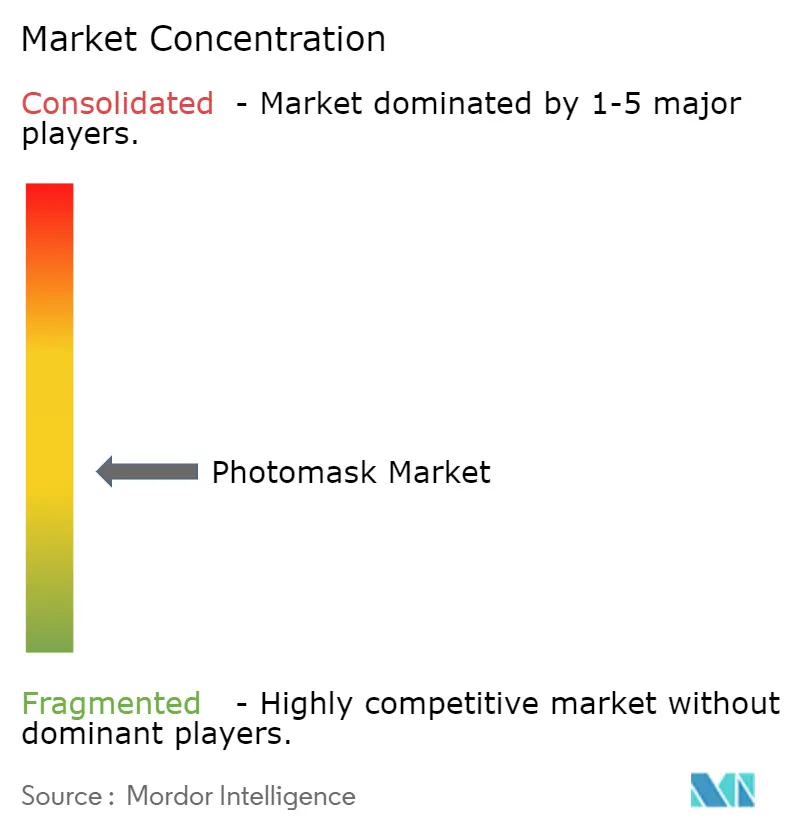
| Market Concentration | Medium |
Major Players*Disclaimer: Major Players sorted in no particular order Image © Mordor Intelligence. Reuse requires attribution under CC BY 4.0. |
|
Photomask Market Analysis by Mordor Intelligence
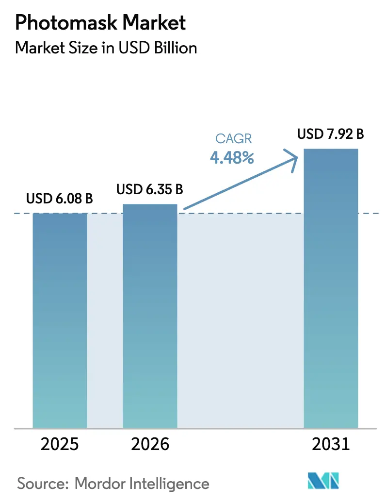
The photomask market size was valued at USD 6.08 billion in 2025 and estimated to grow from USD 6.35 billion in 2026 to reach USD 7.92 billion by 2031, at a CAGR of 4.48% during the forecast period (2026-2031). Sustained demand for higher-resolution reticles, tighter critical-dimension control and defect-free mask blanks underpins this steady growth. Accelerated deployment of High-NA EUV tools in Taiwan and Korea is lifting average selling prices because every successive lithography node requires more sophisticated phase-shift engineering and absorber materials.[1]CommonWealth Magazine, “Taiwan Enters Angstrom Era with ASML's High-NA EUV,” english.cw.com.tw The photomask market also benefits from the global push to localize semiconductor supply chains; new fabs in the United States and the European Union are choosing merchant mask outsourcing over in-house shops to optimize capital efficiency.[2]Peterson Institute for International Economics, “Working Paper 24-3: Semiconductors and Modern Industrial Policy,” piie.com Meanwhile, chiplet-based designs spur incremental demand for redistribution-layer (RDL) and interposer masks, spreading photomask consumption beyond front-end wafer processing into advanced packaging. Display panel makers moving to Gen 8+ AMOLED lines add another vector of growth because each new line consumes up to 30 unique display masks, elevating layer counts and revenue per fab.[3]Journal of Information Display, “Advances in Display Technology…,” tandfonline.com
Key Report Takeaways
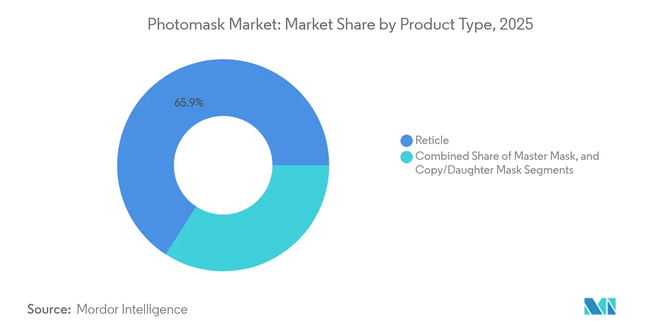
- By product type, reticles led with 65.90% revenue share in 2025; master masks are projected to expand at a 4.99% CAGR to 2031.
- By mask type, binary chrome masks held 43.90% of the photomask market share in 2025, while EUV masks record the highest projected CAGR at 5.29% through 2031.
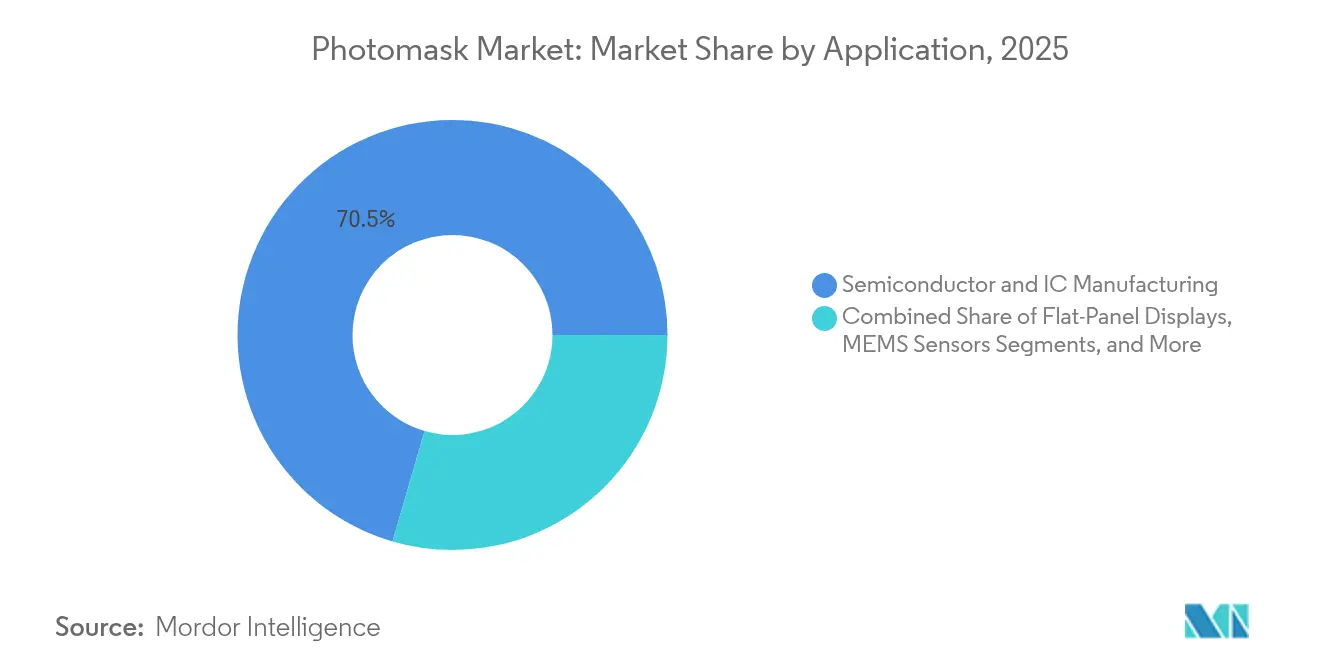
- By application, semiconductor and IC manufacturing accounted for 70.50% of the photomask market size in 2025 and advanced packaging is advancing at a 6.08% CAGR to 2031.
- By end-use industry, foundries and IDMs represented 58.60% of demand in 2025; display panel manufacturers post the fastest 6.39% CAGR to 2031.
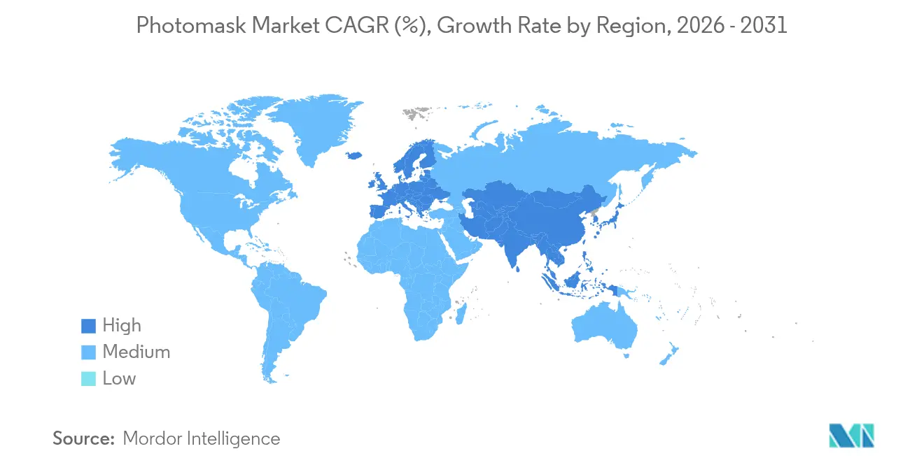
- By geography, Asia-Pacific commanded 71.10% of the photomask market share in 2025, whereas Europe is forecast to grow at a 4.55% CAGR through 2031.
Note: Market size and forecast figures in this report are generated using Mordor Intelligence’s proprietary estimation framework, updated with the latest available data and insights as of 2026.
Global Photomask Market Trends and Insights
Drivers Impact Analysis*
| Driver | (~) % Impact on CAGR Forecast | Geographic Relevance | Impact Timeline |
|---|---|---|---|
| High-NA EUV lithography adoption in Taiwan and Korea | +1.20% | Taiwan, Korea; spillover China | Medium term (2-4 years) |
| U.S./EU CHIPS Acts fueling merchant mask outsourcing | +0.80% | North America & EU; APAC supply chain impact | Long term (≥ 4 years) |
| AMOLED Gen 8+ fabs driving 30-layer display masks | +0.60% | Korea, China; expanding Southeast Asia | Short term (≤ 2 years) |
| Chiplet RDL and interposer photomasks upsurge | +0.70% | APAC core; early adoption North America | Medium term (2-4 years) |
| ADAS & power-semi <28 nm demand for large-area reticles | +0.40% | Global; automotive hubs concentrated | Medium term (2-4 years) |
| AI-enabled defect inspection cutting TAT for captive shops | +0.30% | Global; early use in leading fabs | Short term (≤ 2 years) |
| Source: Mordor Intelligence | |||
High-NA EUV lithography adoption in Taiwan and Korea
Aggressive rollout of High-NA EUV tools marks the industry’s transition into the angstrom era, forcing mask makers to deliver sub-10 nm pattern fidelity with near-zero printable defects. TSMC and Samsung now pay three to four times more per High-NA mask than for conventional EUV sets, expanding supplier revenue even as unit volumes stay stable. Korea’s USD 471 billion semiconductor cluster plan includes captive photomask infrastructure, lowering import reliance and reshaping regional logistics.[4]Korea Times, “Korea Unveils Plan to Build $471 Billion Mega Chip Cluster in Gyeonggi Province,” koreatimes.co.kr Tier-two foundries in China are expected to follow with delayed but inevitable adoption once export-control barriers ease. These developments collectively widen the technology gap between leading-edge and legacy photomask production, pushing legacy margins downward while boosting high-end profitability.
U.S./EU CHIPS Acts fueling merchant mask outsourcing
Domestic incentive programs worth USD 52.7 billion in the United States and comparable measures in Europe encourage new fabs that lack scale to build proprietary mask shops. Merchant suppliers are responding by colocating cleanrooms next to advanced fabs in Arizona, Ohio, and Dresden, improving cycle-times and geopolitical resilience. The regionalization thrust reduces over-dependence on Asia-Pacific sources, a strategic imperative amid rising tensions. Early outsourcing contracts stipulate dedicated toolsets for 3 nm and 2 nm nodes, locking in long-term revenue streams. Over time, merchant providers gain bargaining power as more single-site captive shops shutter to conserve capital.
AMOLED Gen 8+ fabs driving 30-layer display masks
Large-format AMOLED production requires up to 30 fine-aligned layers, a 50% jump from LCD processes, which amplifies mask counts and boosts average selling prices. Samsung Display and LG Display are scaling Gen 8.6 lines for premium tablet and automotive panels, triggering urgent orders for high-resolution pixel masks that minimize color-shift artifacts. Chinese panel makers follow suit to win share in foldable and in-car displays, lengthening the demand runway. Each new line lifts photomask consumption per plant, cushioning suppliers against cyclical dips in smartphone demand. Faster mask-writing platforms with multibeam engines shorten delivery from days to hours, sustaining throughput at peak layer counts.
Chiplet RDL and interposer photomasks upsurge
Heterogeneous integration drives a surge of masks for copper-filled through-silicon vias, micro-bump arrays and redistribution routing that tie chiplets together. TSMC’s Wafer Manufacturing 2.0 concept integrates advanced packaging inside the wafer fab, embedding photomask orders directly into back-end flows. Compared with front-end masks, RDL sets cover larger wafer areas yet need micron-level precision, so suppliers invest in new writers that handle both large substrates and fine pitches. The USD 40 billion chiplet economy therefore translates into meaningful incremental mask revenue. Early adopters in data-center, AI accelerator and RF front-end markets validate the business case, prompting broader uptake.
Restraints Impact Analysis*
| Restraint | (~) % Impact on CAGR Forecast | Geographic Relevance | Impact Timeline |
|---|---|---|---|
| EUV mask-blank defectivity > 5 defects/cm² escalating scrap | −0.9% | Global; acute at leading-edge fabs | Short term (≤ 2 years) |
| Japan quartz-substrate supply bottlenecks | −0.6% | Global; severe for APAC chains | Medium term (2-4 years) |
| Export controls on multi-beam writers limiting China | −0.4% | China; secondary effects worldwide | Long term (≥ 4 years) |
| Rising electricity tariffs in Korea and Taiwan | −0.3% | Korea & Taiwan; cost pass-through global | Medium term (2-4 years) |
| Source: Mordor Intelligence | |||
EUV mask-blank defectivity above 5 defects/cm² escalating scrap
Defect densities beyond the 5 defects/cm² threshold force fabs to scrap up to 25% of EUV mask blanks, inflating costs by USD 50,000–100,000 each and delaying tape-out schedules. Limited qualified suppliers-mainly AGC and Shin-Etsu-struggle to scale volumes while meeting tighter specifications. Although new inspection optics and cleaning recipes lower particle counts, the road to sub-2 defects/cm² remains uncertain. Persistent scrap erodes supplier margins and strains fab ramp-ups slated for 2025–2026. Any prolonged shortage could stall high-end mask deliveries and temper the photomask market CAGR.
Japan quartz-substrate supply bottlenecks
Shin-Etsu and Tosoh control over 80% of ultra-low-expansion quartz substrates, and fresh capacity from Shin-Etsu’s USD 545 million Gunma project will not arrive until 2026. Demand for larger High-NA reticles rises 40-60% per mask, deepening the gap. Geopolitical sensitivities add risk if export curbs widen. Photomask firms compensate by holding extra inventory and lengthening lead times, raising working-capital burdens. Over the medium term, diversified sourcing or glass-ceramic alternatives could relieve pressure, but adoption timetables remain unclear.
*Our forecasts treat driver/restraint impacts as directional, not additive. The impact forecasts reflect baseline growth, mix effects, and variable interactions.
Segment Analysis
By Product Type: Reticles Drive Advanced Node Demand
Reticles generated the bulk of 2025 revenue, holding 65.90% of the photomask market, because every critical layer at sub-10 nm requires flawless image transfer to maintain line-edge roughness within spec. Premium pricing stems from the need to offset sophisticated resist interactions and phase-shift tuning. As High-NA EUV progresses, each device layer often demands bespoke illumination, expanding mask counts per wafer start. Master masks are growing fastest at a 4.99% CAGR because multi-patterning flows require high-fidelity templates that feed step-and-repeat daughter mask production. Copy and daughter masks still address legacy nodes but show subdued volume growth as advanced nodes take center stage. Collectively, the photomask market size for reticles and masters is expected to rise in tandem with wafer starts through 2031.
DNP’s successful demonstration of EUV masks for beyond-2 nm processes underscores how product innovation secures competitive advantage. Reticle suppliers now integrate AI-based defect prediction to lower re-spin rates, improving fab cycle time. Volume manufacturing clusters in Taiwan and Korea favor vendors that can preload inventory near fabs for same-day deliveries, prompting investment in regional satellite sites. Given the high switching costs, customer loyalty remains strong once technical qualification is achieved, preserving revenue visibility across process generations.


By Mask Type: EUV Masks Accelerate Despite Binary Chrome Dominance
Binary chrome masks held the largest 43.90% slice of the photomask market in 2025 thanks to cost-efficient manufacturing that continues to serve 65 nm and older nodes plus most display layers. Their enduring relevance anchors supplier cash flows during market lulls. EUV masks, however, carry the fastest 5.29% CAGR, fueled by sub-3 nm process ramps at foundries and IDMs. Each EUV mask sells at a multiple of optical chrome pricing, magnifying revenue despite lower unit volume. Attenuated and alternating phase-shift masks complement optical flows for critical layers, while nano-imprint templates establish a niche in memory patterning by offering high-throughput, low-cost alternatives when feature uniformity tolerates imprint variability.
The photomask market size for EUV products should expand as memory makers migrate select layers to EUV, adding density without new lithography options. Canon’s nano-imprint roadmap keeps downward pressure on EUV pricing by signaling a substitute for specific applications, but EUV retains higher flexibility and throughput for diverse pattern geometries. Suppliers balance portfolios by keeping chrome capacity viable while funneling capital expenditures toward multibeam writers and pellicle lines required for EUV.
By Application: Advanced Packaging Emerges as Growth Engine
Semiconductor and IC manufacturing held 70.50% revenue share in 2025, reflecting the central role of front-end wafer processing in driving photomask demand. Yet advanced packaging shows the most robust 6.08% CAGR because chiplet architectures need multiple RDL and interposer layers per component. The photomask market size for advanced packaging is projected to expand at 6.08% CAGR between 2026 and 2031. Display manufacturing-LCD, AMOLED and emerging micro-OLED-continues to procure large-area masks even as panel prices fluctuate. MEMS, photonics and sensor applications provide steady, albeit smaller, volumes that call for ultra-high aspect-ratio patterns or double-expose flows.
Packaging masks differ from front-end sets in substrate size and alignment requirements, pushing vendors to procure oversized writers and metrology gear. Heterogeneous integration’s rise means packaging plants now place mask orders in numbers once reserved for wafer fabs, narrowing the historical gap. Suppliers that cross-bundle optical and EUV masks with packaging sets secure comprehensive contracts and create stickier relationships. Customization around die-to-wafer and fan-out architectures further boosts engineering service revenue, complementing mask sales.
By End-use Industry: Display Manufacturers Accelerate Growth
Foundries and IDMs dominated offtake in 2025 at 58.60% because they control the highest wafer volumes and most advanced lithography nodes, driving recurring large-lot orders. Nonetheless, display panel manufacturers register the quickest 6.39% CAGR as Gen 8+ AMOLED capacity expands in Korea and China, multiplying layer counts and tightening overlay tolerances. Fabless design houses remain integral though they purchase masks indirectly via foundry partners, so their influence shows up in technology specifications rather than direct procurement. Outsourced semiconductor assembly and test (OSAT) companies raise photomask demand as they migrate toward 3DIC interposers, ensuring device stack integrity. Research institutions and aerospace customers buy small but technically demanding mask sets, maintaining niche revenue streams.
Momentum in display drives suppliers to refine phase-shift techniques that mitigate mura and enhance pixel uniformity, keyed to emerging automotive cockpit standards. IDMs focus on cost and delivery assurance, often signing multi-year master service agreements. OSAT expansions in Southeast Asia bring new regional mask hubs online, diversifying geographic revenue distribution. This widening customer base supports resilient growth even if one vertical softens cyclically.
Geography Analysis
Asia-Pacific secured 71.10% of global sales in 2025 because Taiwan, Korea and China host the densest concentration of cutting-edge fabs and the most complete mask-making ecosystem. TSMC alone represents more than 60% of global foundry revenue, commanding massive reticle volumes each quarter. Complementary supply chains-quartz substrates from Shin-Etsu Chemical, multibeam writers from NuFlare and repair tools from Mycronic-enable same-region procurement, minimizing cycle-time risk. China continues adding mature-node capacity at a double-digit clip despite export constraints, ensuring ongoing demand for optical chrome masks. Korea’s USD 471 billion cluster plan adds 16 new fabs through 2047, each with dedicated photomask infrastructure, reinforcing Asia-Pacific pre-eminence.
Europe is growing fastest at 4.55% CAGR as governments fund semiconductor sovereignty programs under the European Chips Act. Tekscend Photomask’s multibeam installation in Dresden cuts writing time for complex masks from days to mere hours, signaling continental readiness for advanced-node production. Germany anchors the region through ZEISS SMT’s expansion of mask-solutions sites in Jena, Oberkochen and Wetzlar, aligning optics, blanks and writing to local fab needs. Strategic focus rests on automotive and industrial chips, where Europe already wields design and systems expertise, augmenting domestic photomask uptake.
North America benefits from USD 52.7 billion in CHIPS Act incentives that spur fab projects in Arizona, Ohio and New York, creating fresh demand for proximate mask suppliers. TSMC’s USD 165 billion Arizona complex alone will consume thousands of EUV masks annually, inviting both Asian and European vendors to establish local satellite operations. Intel’s foundry push, GlobalFoundries’ expansions and multiple specialty fabs together diversify the customer base. However, cost structures remain higher than in Asia-Pacific, so profit margins depend on value-added services such as rapid-turn prototypes and on-site defect analysis.

Competitive Landscape
The photomask market remains moderately consolidated because capital intensity and technology hurdles deter new entrants. Toppan (via Tekscend), Dai Nippon Printing and Photronics anchor the top tier, each operating multibeam writer fleets for EUV, aggressive phase-shift libraries and comprehensive inspection loops. DNP’s delivery of beyond-2 nm EUV masks validates its R&D advantage and satisfies leading-edge qualification requirements. Photronics notes resilient demand for high-end IC and flat-panel masks even during cyclical soft patches, reflecting the secular trend toward higher-layer complexity.
Geographic diversification is the new battleground. Tekscend’s Dresden facility, Photronics’ expansion in Xiamen and anticipated moves into the United States highlight efforts to shield revenue from geopolitical risks while aligning with customer localization mandates. Mycronic’s July 2025 acquisition of Cowin DST in Korea enhances repair capabilities and strengthens its footprint among display and semiconductor clients. An adjacent wave of equipment suppliers-including KLA, ZEISS and DuPont-expands regional factories to support mask makers with inspection, pellicles and resist materials, tightening ecosystem coupling.
Technology roadmaps now prioritize AI-enabled defect detection that slashes measurement time and reduces re-spins. Multibeam writers capable of handling 7 nm sub-crescent features enter volume production, pushing productivity beyond legacy electron-beam tools. Alternative patterning such as nano-imprint lithography threatens selective displacement but still faces scalability and pellicle challenges. Overall rivalry intensifies around advanced packaging masks, where few incumbents possess oversized writers or wide-field optics-alignment expertise, opening white-space territory for nimble specialists.
Photomask Industry Leaders
-
Tekscend Photomask Inc.
-
Dai Nippon Printing Co., Ltd.
-
Photronics, Inc.
-
Hoya Corporation
-
SK-Electronics Co., Ltd.
- *Disclaimer: Major Players sorted in no particular order

Recent Industry Developments
- July 2025: Mycronic AB’s Pattern Generators division acquired Cowin DST, a South Korean photomask-repair specialist, adding USD 10 million projected 2025 revenue.
- July 2025: Cica-Huntek Chemical Technology Taiwan injected USD 123 million into its US subsidiary to support dispense systems for 3 nm and 5 nm fabs.
- March 2025: Imec and ZEISS extended their Strategic Partnership Agreement to 2029, backing sub-2 nm R&D and the NanoIC pilot line.
- January 2025: TSMC received ASML High-NA EUV tools, ushering Taiwan into the angstrom era of lithography.
- December 2024: Dai Nippon Printing began supplying evaluation EUV masks compatible with High-NA tools for beyond-2 nm nodes.


Global Photomask Market Report Scope
The photomask market encompasses the production and supply of high-precision plates or templates used in photolithography to transfer circuit patterns onto semiconductor wafers, flat-panel displays, and MEMS devices. Photomasks are essential for the fabrication of advanced chips and electronic components, enabling precise patterning and scaling. The market's growth is driven by advancements in semiconductor technology, increasing complexity of designs, and the adoption of new lithography techniques like EUV.
The Photomask Market is segmented by product type (reticle, master mask, copy mask), mask type (binary mask, phase shift mask (PSM), extreme ultraviolet (EUV) mask, other mask types), application (semiconductor and IC manufacturing, flat-panel displays, mems devices, other application), end-use industry (electronics, automotive, telecommunications, aerospace & defense, other end-use industries), and geography (North America, Europe, Asia Pacific, Latin America, Middle East and Africa). The market sizes and forecasts are provided in terms of value (USD) for all the above segments.
| Reticle (4×/5×) |
| Master Mask |
| Copy/Daughter Mask |
| Binary Chrome Mask (BCM) |
| Attenuated Phase Shift Mask (Att-PSM) |
| Alternating Phase Shift Mask (Alt-PSM) |
| Chromeless Phase Lithography Mask |
| EUV Photomask |
| Nano-imprint Template |
| Semiconductor and IC Manufacturing | More than 65 nm |
| 45-28 nm | |
| 22-14 nm | |
| 10-7 nm | |
| 5 nm | |
| Upto 3 nm | |
| Flat-Panel Displays | LCD |
| AMOLED | |
| OLED Micro-display | |
| MEMS Sensors | |
| Advanced Packaging (RDL/Interposer) | |
| Photonics and Silicon Photonics | |
| Others |
| Foundries and IDMs |
| Fabless Design Houses |
| Display Panel Manufacturers |
| OSAT/Advanced Packaging Providers |
| Research and Academia |
| Aerospace and Defense |
| Telecommunications OEMs |
| North America | United States | |
| Canada | ||
| Mexico | ||
| Europe | Germany | |
| United Kingdom | ||
| France | ||
| Nordics | ||
| Rest of Europe | ||
| South America | Brazil | |
| Rest of South America | ||
| Asia-Pacific | China | |
| Japan | ||
| India | ||
| South-East Asia | ||
| Rest of Asia-Pacific | ||
| Middle East and Africa | Middle East | Gulf Cooperation Council Countries |
| Turkey | ||
| Rest of Middle East | ||
| Africa | South Africa | |
| Rest of Africa | ||
| By Product Type | Reticle (4×/5×) | ||
| Master Mask | |||
| Copy/Daughter Mask | |||
| By Mask Type | Binary Chrome Mask (BCM) | ||
| Attenuated Phase Shift Mask (Att-PSM) | |||
| Alternating Phase Shift Mask (Alt-PSM) | |||
| Chromeless Phase Lithography Mask | |||
| EUV Photomask | |||
| Nano-imprint Template | |||
| By Application | Semiconductor and IC Manufacturing | More than 65 nm | |
| 45-28 nm | |||
| 22-14 nm | |||
| 10-7 nm | |||
| 5 nm | |||
| Upto 3 nm | |||
| Flat-Panel Displays | LCD | ||
| AMOLED | |||
| OLED Micro-display | |||
| MEMS Sensors | |||
| Advanced Packaging (RDL/Interposer) | |||
| Photonics and Silicon Photonics | |||
| Others | |||
| By End-use Industry | Foundries and IDMs | ||
| Fabless Design Houses | |||
| Display Panel Manufacturers | |||
| OSAT/Advanced Packaging Providers | |||
| Research and Academia | |||
| Aerospace and Defense | |||
| Telecommunications OEMs | |||
| By Geography | North America | United States | |
| Canada | |||
| Mexico | |||
| Europe | Germany | ||
| United Kingdom | |||
| France | |||
| Nordics | |||
| Rest of Europe | |||
| South America | Brazil | ||
| Rest of South America | |||
| Asia-Pacific | China | ||
| Japan | |||
| India | |||
| South-East Asia | |||
| Rest of Asia-Pacific | |||
| Middle East and Africa | Middle East | Gulf Cooperation Council Countries | |
| Turkey | |||
| Rest of Middle East | |||
| Africa | South Africa | ||
| Rest of Africa | |||


Key Questions Answered in the Report
What is the current value of the photomask market?
The photomask market stands at USD 6.35 billion in 2026 and is projected to reach USD 7.92 billion by 2031.
Which region leads the photomask market?
Asia-Pacific dominates with 71.10% market share in 2025, underpinned by Taiwan’s and Korea’s advanced fabs.
Why are EUV photomasks gaining importance?
Foundries ramping sub-3 nm nodes need EUV masks for finer patterns and improved throughput, driving the segment’s 5.29% CAGR.
How will the CHIPS Acts influence photomask demand?
Incentives in the United States and Europe spur merchant mask outsourcing, adding localized demand near new fabs.
Which application is growing fastest for photomasks?
Advanced packaging masks for RDL and interposers grow at 6.08% CAGR due to chiplet-based architectures.
What challenge does quartz substrate shortage pose?
Limited high-purity quartz capacity in Japan heightens lead times and costs for High-NA EUV photomasks until new lines come online in 2026.
Page last updated on:


