Photosensitive Semiconductor Device Market Size and Share
Market Overview
| Study Period | 2020 - 2031 |
|---|---|
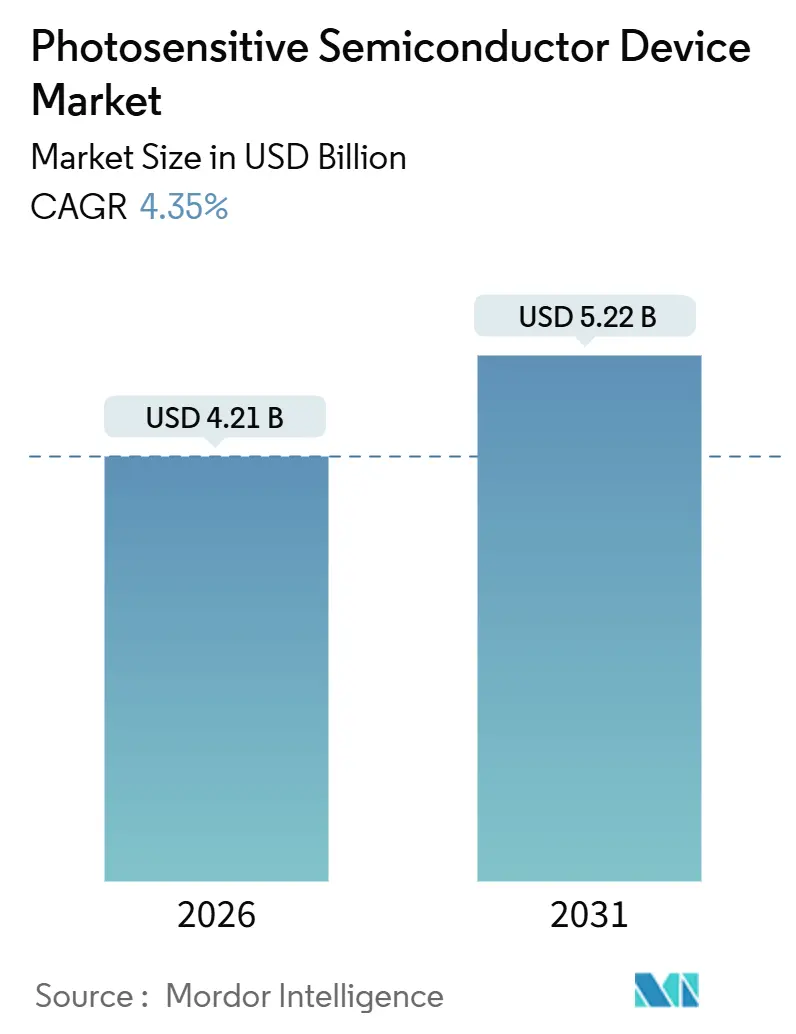
| Market Size (2026) | USD 4.21 Billion |
| Market Size (2031) | USD 5.22 Billion |
| Growth Rate (2026 - 2031) | 4.35% CAGR |
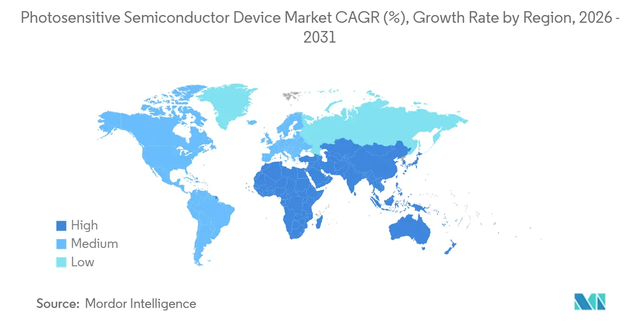
| Fastest Growing Market | Asia Pacific |
| Largest Market | Asia Pacific |
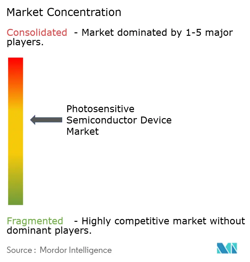
| Market Concentration | Medium |
Major Players *Disclaimer: Major Players sorted in no particular order Image © Mordor Intelligence. Reuse requires attribution under CC BY 4.0. | |
Photosensitive Semiconductor Device Market Analysis by Mordor Intelligence
The photosensitive semiconductor device market size reached USD 4.21 billion in 2026 and is projected to grow to USD 5.22 billion by 2031, reflecting a 4.35% CAGR over the forecast period. Robust LiDAR demand from automotive original-equipment manufacturers, the pivot toward on-sensor artificial-intelligence processing, and ongoing material innovation are reshaping product design and pricing. Automakers are standardizing time-of-flight ranging in Level 3 driver-assistance systems, smartphone makers are extending multi-camera arrays to mid-tier handsets, and research consortia are proving perovskite and organic photodetectors with external quantum efficiency beyond 80% in the near-infrared spectrum. These forces accelerate the shift from commodity imaging toward mission-critical sensing, while simultaneously pressuring suppliers to reduce power consumption and footprint. Asia Pacific leads revenue thanks to concentrated electric-vehicle output and consumer-electronics assembly, but supply-chain risks linger around ultra-high-purity silicon wafers and automotive reflow reliability.
Key Report Takeaways
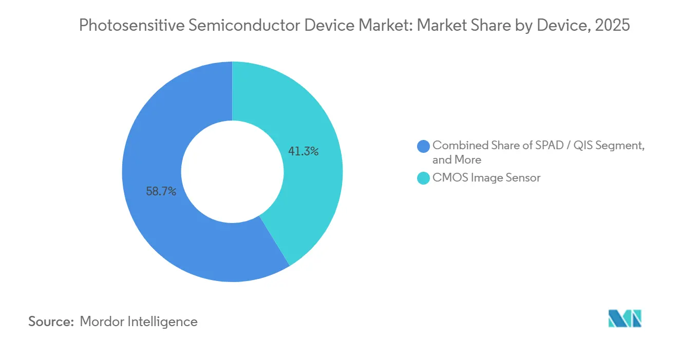
- By device, CMOS image sensors led with 41.28% revenue share in 2025, and single-photon avalanche diode arrays are advancing at a 4.89% CAGR through 2031.
- By material, silicon held 62.16% of the photosensitive semiconductor device market share in 2025, while perovskite and other emerging compounds are forecast to expand at 5.12% through 2031.
- By operating mode, photovoltaic architectures accounted for 54.03% of 2025 shipments and avalanche mode is set to increase at 5.54% between 2026-2031.
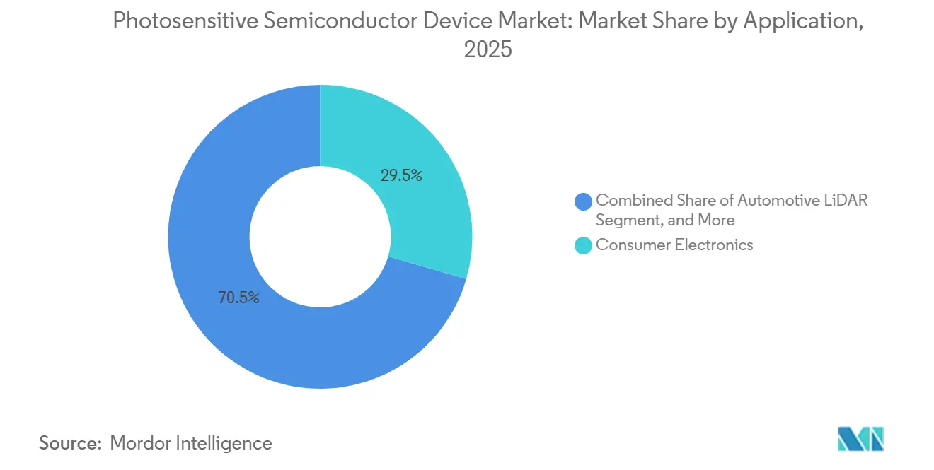
- By application, consumer electronics captured 29.48% of value in 2025, whereas the automotive LiDAR subsegment is expected to grow at a 5.89% CAGR to 2031.
- By geography, Asia Pacific held 44.17% revenue share in 2025 and is projected to climb at 5.81% through 2031.
Note: Market size and forecast figures in this report are generated using Mordor Intelligence’s proprietary estimation framework, updated with the latest available data and insights as of January 2026.
Global Photosensitive Semiconductor Device Market Trends and Insights
Drivers Impact Analysis*
| Driver | (~) % Impact on CAGR Forecast | Geographic Relevance | Impact Timeline |
|---|---|---|---|
| Rising Automotive ADAS and LiDAR Adoption | +1.20% | Global, with concentration in China, EU, and North America | Medium term (2-4 years) |
| Exploding Multi-Camera Smartphone Shipments | +0.90% | APAC core, spill-over to North America and Europe | Short term (≤ 2 years) |
| Demand for Improved Imaging and Optical Sensing | +0.70% | Global | Medium term (2-4 years) |
| Long Life and Low Power Consumption | +0.50% | Global, emphasis on consumer electronics and IoT hubs | Long term (≥ 4 years) |
| Emergence of Organic Photodetectors for Flexible Electronics | +0.40% | APAC (Japan, South Korea), early adoption in North America | Long term (≥ 4 years) |
| On-Sensor AI Processing Reducing Bandwidth and System Cost | +0.80% | Global, led by smartphone and automotive OEMs | Medium term (2-4 years) |
| Source: Mordor Intelligence | |||
Rising Automotive ADAS and LiDAR Adoption
LiDAR unit shipments reached 830,000 during the first three quarters of 2025 as Chinese sport-utility vehicles priced below USD 40,000 adopted solid-state scanners.[1]Hesai Group, “Third Quarter 2025 Investor Presentation,” hesai.com European regulations requiring automatic emergency braking by model-year 2027 are accelerating avalanche-photodiode demand in forward-facing camera clusters. North American tier-one suppliers increased purchase orders by 40% in late 2025, driven by rollouts from General Motors and Ford. Time-of-flight arrays need sub-10-nanosecond response, creating a moat for incumbents that already hold AEC-Q101 qualifications. Unit prices have fallen roughly 60% since 2024, expanding addressable volume but squeezing margins for photodetector vendors.
Exploding Multi-Camera Smartphone Shipments
Handsets with three or more rear cameras surpassed 720 million units in 2025, up from 580 million in 2024, as mid-tier Android models adopted ultra-wide and telephoto modules.[2]Sony Semiconductor Solutions, “Annual Report Fiscal 2025,” sony-semicon.com Sony’s stacked sensors integrate phase-detection pixels and high-dynamic-range processing, while Samsung’s ISOCELL GNJ shrinks module height by 8%. Chinese brands now specify back-side-illuminated arrays with on-chip analog-to-digital conversion that cuts power draw by 20%, meeting battery-life constraints imposed by 5G modems. Alignment of ISO 12233 and IEEE P2020 standards is allowing dual-use designs for smartphones and in-cabin monitoring, speeding product reuse.
On-Sensor AI Processing Reducing Bandwidth and System Cost
Prototypes demonstrated in 2025 cut system-level data traffic by up to 75%, since neural-network inference runs inside the sensor die. Sony’s IMX500, capable of 3.1 TOPS, entered volume production mid-2025 and saw early uptake in warehouse robots and retail analytics. OmniVision followed with an automotive driver-monitoring variant, targeting Euro NCAP 2026 protocols. Eliminating external image-signal processors reduces printed-circuit-board area by one-third and power by up to 40%. However, meeting ISO 26262 functional-safety targets adds nine months of validation and raises non-recurring engineering costs.
Demand for Improved Imaging and Optical Sensing
Edge-device makers require wider dynamic range, higher quantum efficiency, and lower dark current to unlock advanced functions such as gaze tracking and spectral analysis. Stacked architectures separate pixel and logic wafers, increasing full-well capacity, while per-pixel analog-to-digital converters raise signal-to-noise ratios above 70 decibels. In industrial automation, machine-vision systems now inspect surface defects smaller than 5 micrometers, pushing suppliers toward global-shutter pixels and on-chip HDR fusion. Medical device OEMs demand photon-counting sensitivity for computed-tomography scanners, another tailwind for single-photon avalanche diode arrays.
Restraints Impact Analysis*
| Restraint | (~) % Impact on CAGR Forecast | Geographic Relevance | Impact Timeline |
|---|---|---|---|
| Increasing Price Pressure | -0.80% | Global, most acute in consumer electronics and mid-tier automotive | Short term (≤ 2 years) |
| Competition from Alternative Sensing Technologies | -0.50% | North America and Europe, moderate in APAC | Medium term (2-4 years) |
| Photodiode Reliability Issues During Automotive Reflow Cycles | -0.40% | Global automotive supply chains | Medium term (2-4 years) |
| Limited Supply of Ultra-High-Purity Silicon Wafers | -0.60% | Global, concentrated impact on high-performance discrete devices | Long term (≥ 4 years) |
| Source: Mordor Intelligence | |||
Increasing Price Pressure
Average selling prices for mainstream CMOS sensors fell 12% between Q4 2024 and Q3 2025 as Chinese startups undercut incumbents.[4]OmniVision Technologies, “Q3 2025 Earnings Call Transcript,” ovt.com Automotive integrators now expect annual 5-7% unit cost reductions, eroding margins for discrete photodiodes. Computational photography extends flagship-level image quality to lower-resolution sensors, dampening hardware upgrades. System-on-chip integration shifts value toward foundry partners, leaving traditional sensor vendors with a shrinking share of the bill-of-material.
Limited Supply of Ultra-High-Purity Silicon Wafers
Three Japanese suppliers control roughly 85% of 6-inch and 8-inch high-resistivity wafer output, and lead times stretched from 16 weeks in early 2024 to 28 weeks by Q3 2025. Supply tightness forces photodiode makers to prioritize premium aerospace and medical customers over consumer applications. Contaminants degrade dark current in avalanche devices, so substitution with germanium-on-silicon or silicon-carbide wafers remains experimental. Any disruption to Japanese wafer production would ripple through global LiDAR programs within three months.
*Our forecasts treat driver/restraint impacts as directional, not additive. The impact forecasts reflect baseline growth, mix effects, and variable interactions.
Segment Analysis
By Device: Stacked Sensors Anchor Share, SPAD Arrays Drive Growth
CMOS image sensors contributed 41.28% of 2025 revenue and remain the volume backbone of the photosensitive semiconductor device market. Their dominance rests on stacked architectures that decouple pixel and logic wafers, allowing larger full-well capacity, faster readout, and on-sensor artificial-intelligence blocks that remove external signal processors. Sony, Samsung, and SK hynix collectively shipped more than 100 million stacked units in 2025, enabling 8 K video at 60 frames per second and sustained 480-frame bursts for computational photography. Back-side-illuminated layouts now cover roughly 70% of smartphone output, a jump from 55% in 2023, as mid-tier Android handsets demanded sub-0.7 micrometer pixels to preserve low-light sensitivity. The photosensitive semiconductor device market size tied to stacked sensors is forecast to rise from USD 1.74 billion in 2026 to USD 2.15 billion by 2031, supported by continued camera proliferation in wearables and drones.
Discrete photodiodes PIN, PN, avalanche, and Schottky variants occupy a resilient niche in optical communication, medical imaging, and industrial automation, where spectral customization and AEC-Q101 validation outweigh the integration advantages of image sensors. Single-photon avalanche diode and quantum image sensor arrays exhibit the fastest trajectory, advancing at a 4.89% CAGR as automakers and lidar makers require picosecond timing precision. Photo-ICs that merge photodiodes with transimpedance amplifiers and comparators are expanding in health-monitoring patches and augmented-reality headsets because they cut board area by half and power draw by one-third. In contrast, phototransistors, photoresistors, and legacy photocells account for under 2% of photosensitive semiconductor device market share and are slowly retreating to low-speed optocouplers and ambient-light modules. Reliability in automotive reflow remains an open challenge; forward-voltage drift forced suppliers to specify tighter junction-capacitance windows and dark-current ceilings, raising test cost but preserving field performance.


By Material: Silicon Dominates, Perovskites Promise Disruption
Silicon held 62.16% of 2025 value because decades of complementary metal-oxide-semiconductor process tuning keep defect densities low and cost per pixel unmatched. Its grip is strongest in smartphones, automotive surround-view cameras, and machine-vision systems, where wafer tooling and circuit libraries are highly amortized. Even so, marginal cost gains are tapering as pixel pitch nears 0.5 micrometers and quantum-efficiency ceilings approach 95% in the visible band. Suppliers are therefore stretching silicon through advanced doping profiles, backside deep-trench isolation, and wafer bonding to retain competitiveness. The photosensitive semiconductor device market size linked to silicon is expected to inch upward at a sub-4% CAGR, yet its overall share slips as alternatives mature.
Perovskite and organic semiconductors represent the most credible long-term threat. Research groups in Japan and South Korea reported external quantum efficiency above 80% in the 800–1,200 nanometer band during 2025, performance that undercuts indium gallium arsenide at one-tenth of material cost. Panasonic’s pilot line for dashboard-integrated organic photodiodes illustrates early commercialization, while Hamamatsu and ON Semiconductor have disclosed roadmap evaluations for perovskite avalanche structures that promise internal gain without high reverse bias. Qualification gaps persist because neither IEC 60747 nor AEC-Q101 defines reliability rules for solution-processed layers; tier-one automotive suppliers are crafting bespoke 1,000-hour humidity and UV tests, adding up to 12 months to launch cycles. Germanium and indium gallium arsenide remain entrenched in telecom and spectroscopy, but their premium pricing will face incremental erosion once perovskite detectors prove 10,000-hour stability under 85 °C and 85% relative humidity.
By Operating Mode: Photovoltaic Mode Leads, Avalanche Gains Traction
Photovoltaic operation represented 54.03% of 2025 unit shipments, favored in battery-sensitive smartphones and tablets because zero-bias readout keeps noise below 2 electrons rms. Device makers pair photovoltaic pixels with in-pixel analog-to-digital converters to deliver 40 decibel signal-to-noise ratios at less than 100 milliwatts. The mode’s prevalence anchors cost; wafer lots can tolerate ±10% doping variance, speeding yields. However, bandwidth caps at roughly 1 gigahertz limit suitability for high-speed optical links and time-of-flight ranging.
Photoconductive detectors requiring external bias fill the mid-speed slot in barcode scanners and industrial positioning, yet design wins are migrating to photo-ICs that embed amplifiers and thus neutralize discrete bias circuitry. Avalanche mode exhibits the most compelling upside, advancing at a 5.54% CAGR as automotive lidar migrates from mechanical to solid-state scanning. Internal gain above 100 multiplies weak return photons from 200-meter targets, lowering laser-emitter power budgets and easing eye-safety compliance. The photosensitive semiconductor device market share for avalanche architectures will climb despite tighter epitaxial tolerances that raise wafer cost by 35% and AEC-Q101 validation that demands 1,000-hour high-temperature reverse-bias stress. Suppliers are responding with proprietary guard-ring geometries that suppress edge breakdown and with silicon-on-insulator substrates that curb dark current by up to 40%.
By Application: Consumer Electronics Leads, Automotive LiDAR Surges
Consumer electronics seized 29.48% of 2025 revenue on the back of 1.3 billion smartphone and tablet shipments. Handsets now integrate primary, telephoto, ultra-wide, depth, and macro modules, driving per-device sensor count to five or more. Pixel pitch has fallen below 0.7 micrometers, yet back-side-illuminated designs preserve low-light performance while on-chip high-dynamic-range fusion manages 120-decibel scenes. Smartwatch and hearable adoption adds incremental unit volume, although revenue contribution remains modest given sub-USD 2 average selling prices. Future tailwinds include compact global-shutter arrays for spatial-video capture and on-sensor neural cores that offload image enhancement to edge hardware.
Automotive lidar is on the steepest slope, expanding at a 5.89% CAGR through 2031 as European and Chinese regulations mandate vulnerable-road-user detection. Solid-state arrays now command 60% of new design wins, a reversal from 2023 when rotational units still dominated. Avalanche-photodiode arrays with excess-noise factors under 3 and single-photon avalanche diodes with timing jitter below 100 picoseconds enable object classification at 200 meters in rain or fog. The photosensitive semiconductor device market size attributable to lidar sensors is set to reach USD 0.90 billion by 2031, up from USD 0.68 billion in 2026. Healthcare, industrial automation, and scientific instrumentation collectively form a resilient long-tail, with computed-tomography scanners, collaborative robots, and quantum-optics labs demanding low-volume but high-margin detectors.
By End User: Automotive OEMs and Consumer Electronics OEMs Dominate
Automotive original-equipment manufacturers consumed nearly one-third of 2025 detector shipments as Level 2+ assistance became table stakes in premium sedans and crossovers. Sourcing strategies are tightening: tier-one suppliers require deterministic latency under 5 milliseconds and built-in self-test, elevating bill-of-material cost by 20-25% over consumer-grade sensors. Domain-controller architectures favor centralized processing fed by multiple cameras and lidar channels, pushing suppliers toward standardized MIPI C-PHY and Ethernet-AVB outputs. Warranty cycles span a decade, so AEC-Q101 and ISO 26262 documentation now appears in every request-for-quotation, extending design-in timelines to as long as 24 months but cementing incumbent share once won.
Consumer-electronics OEMs account for another 30% of shipments, but their priorities are inverted: lowest unit cost, thinnest module height, and annual refresh cadences. Pixel pitches below 0.6 micrometers and 16-in-1 binning allow flagship-class low-light imaging even in mid-range devices, eroding the historical premium tier. Suppliers that can stack analog-to-digital converters and neural-processing blocks directly under pixel arrays gain both die-size efficiency and licensing leverage over application-processor vendors. Aerospace and defense contractors, while below 5% of volume, deliver outsized margin with radiation-hardened requirements and multiyear procurement contracts. Healthcare device manufacturers need FDA 510(k) clearance or CE marking, adding 12-18 months to product cycles yet yielding sticky revenue once validation hurdles are cleared.
Geography Analysis
Asia Pacific contributed 44.17% of 2025 revenue and is projected to expand at 5.81% through 2031. Chinese electric-vehicle makers installed more LiDAR units than the rest of the world combined in 2025, while South Korean foundries shipped over 400 million smartphone image sensors. Japanese specialists dominate avalanche photodiodes for medical and scientific systems, and India plus ASEAN states are scaling module assembly although fabrication stays concentrated in China, Japan, South Korea, and Taiwan.
North America generated about 25% of value in 2025, driven by automotive ADAS, data-center optical links, and defense programs. However, the region relies on Japanese epitaxial wafers, exposing it to the same lead-time shocks faced by global peers. Teledyne and ON Semiconductor operate local wafer fabs, yet capacity expansion lags Asia’s scale. Regulatory momentum from the National Highway Traffic Safety Administration for automatic emergency braking is encouraging LiDAR integration, but manufacturing subsidies trail the European Chips Act.
Europe and the Middle East delivered roughly 22% of revenue in 2025. German and French plants adopted surround-view cameras to meet General Safety Regulation mandates, lifting regional image-sensor shipments by 35%. Absence of local LiDAR photodiode suppliers compels automakers to source from Japan and the United States, prompting European policy initiatives to fund joint ventures. South America and Africa combined for under 9% of revenue, with adoption focused on mining automation and telecom backhaul; reliance on imports and exchange-rate volatility constrains growth.

Competitive Landscape
The market displays moderate concentration. Sony Semiconductor Solutions and Samsung System LSI together controlled more than 60% of smartphone image-sensor value in 2025, leveraging stacked pixels and captive foundries. Discrete photodiodes and avalanche devices remain fragmented across Hamamatsu Photonics, ON Semiconductor, Vishay Intertechnology, and niche players. Barriers stem from AEC-Q101 and ISO 26262 validation, plus the need for spectral customization that mass fabs avoid. On-sensor AI accelerators and perovskite photodetectors represent white-space growth, and patent filings for single-photon avalanche diodes jumped 40% between 2024-2025.
Chinese challengers such as GalaxyCore and SmartSens gained roughly 15% of global smartphone sensor volume in 2025 by discounting prices 20-30%. They lack stacked-sensor processes but win domestic Android designs, compressing mid-tier margins. Incumbents counter by focusing on premium features or pivoting to automotive and industrial verticals with longer qualification cycles. Strategic moves include ON Semiconductor’s silicon-carbide expansion, STMicroelectronics’ time-of-flight joint venture with Valeo, and Hamamatsu’s 12-inch wafer fab for silicon photomultipliers. Consolidation is expected within 24 months as capital intensity and system-level expertise requirements rise.
Photosensitive Semiconductor Device Industry Leaders
Sony Corporation
Samsung Electronics Co. Ltd
Canon Inc.
Continental AG
Panasonic Corporation
- *Disclaimer: Major Players sorted in no particular order

Recent Industry Developments
- January 2026: Sony Semiconductor Solutions released the IMX585 stacked CMOS sensor with 4.2 TOPS on-chip AI processing for driver monitoring and machine vision.
- December 2025: Hamamatsu Photonics finished an JPY 18 billion (USD 120 million) Toyooka factory expansion adding 12-inch capacity for silicon photomultipliers and SPAD arrays.
- November 2025: ON Semiconductor and Hesai Group agreed to co-develop avalanche photodiode arrays for sub-USD 500 LiDAR units, with pilot production slated for Q2 2026.
- October 2025: Samsung System LSI introduced the ISOCELL HP7 200-MP image sensor featuring 0.56-µm pixels and 16-in-1 binning for flagship smartphones.


Global Photosensitive Semiconductor Device Market Report Scope
The Photosensitive Semiconductor Device Market Report is Segmented by Device (Photocell, Photodiode, Phototransistor, Photoresistor, Photo IC, CMOS Image Sensor, SPAD/QIS), Material (Silicon, Germanium, Indium Gallium Arsenide, Gallium Arsenide, Organic Semiconductor, Perovskite and Other Emerging Materials), Operating Mode (Photovoltaic, Photoconductive, Avalanche), Application (Optical Communication, Automotive, Consumer Electronics, Healthcare, Industrial Automation, Security, Scientific Research), End User (Automotive OEMs, Consumer Electronics OEMs, Aerospace and Defence Contractors, Healthcare Device Manufacturers, Industrial Firms), and Geography (North America, South America, Europe, Asia Pacific, Middle East, Africa). The Market Forecasts are Provided in Terms of Value (USD).
| Photocell | |
| Photodiode | PIN Photodiode |
| PN Photodiode | |
| Avalanche Photodiode | |
| Schottky Photodiode | |
| Phototransistor | |
| Photoresistor | |
| Photo IC | |
| CMOS Image Sensor | BSI Sensor |
| Stacked Sensor | |
| SPAD / QIS |
| Silicon |
| Germanium |
| Indium Gallium Arsenide |
| Gallium Arsenide |
| Organic Semiconductor |
| Perovskite and Other Emerging Materials |
| Photovoltaic Mode |
| Photoconductive Mode |
| Avalanche Mode |
| Optical Communication and Datacom | |
| Automotive and Transportation | LiDAR |
| ADAS Cameras | |
| Consumer Electronics | Smartphones and Tablets |
| Wearables and AR/VR | |
| Healthcare and Medical Imaging | |
| Industrial Automation and Robotics | |
| Security and Surveillance | |
| Scientific Research and Instrumentation |
| Automotive OEMs |
| Consumer Electronics OEMs |
| Aerospace and Defence Contractors |
| Healthcare Device Manufacturers |
| Industrial and Manufacturing Firms |
| North America | United States |
| Canada | |
| Mexico | |
| South America | Brazil |
| Argentina | |
| Europe | Germany |
| France | |
| United Kingdom | |
| Italy | |
| Spain | |
| Russia | |
| Rest of Europe | |
| Asia Pacific | China |
| Japan | |
| India | |
| South Korea | |
| ASEAN | |
| Oceania | |
| Middle East | GCC |
| Turkey | |
| Rest of Middle East | |
| AFRICA | South Africa |
| North Africa | |
| Rest of Africa |
| By Device | Photocell | |
| Photodiode | PIN Photodiode | |
| PN Photodiode | ||
| Avalanche Photodiode | ||
| Schottky Photodiode | ||
| Phototransistor | ||
| Photoresistor | ||
| Photo IC | ||
| CMOS Image Sensor | BSI Sensor | |
| Stacked Sensor | ||
| SPAD / QIS | ||
| By Material | Silicon | |
| Germanium | ||
| Indium Gallium Arsenide | ||
| Gallium Arsenide | ||
| Organic Semiconductor | ||
| Perovskite and Other Emerging Materials | ||
| By Operating Mode | Photovoltaic Mode | |
| Photoconductive Mode | ||
| Avalanche Mode | ||
| By Application | Optical Communication and Datacom | |
| Automotive and Transportation | LiDAR | |
| ADAS Cameras | ||
| Consumer Electronics | Smartphones and Tablets | |
| Wearables and AR/VR | ||
| Healthcare and Medical Imaging | ||
| Industrial Automation and Robotics | ||
| Security and Surveillance | ||
| Scientific Research and Instrumentation | ||
| By End User | Automotive OEMs | |
| Consumer Electronics OEMs | ||
| Aerospace and Defence Contractors | ||
| Healthcare Device Manufacturers | ||
| Industrial and Manufacturing Firms | ||
| By Geography | North America | United States |
| Canada | ||
| Mexico | ||
| South America | Brazil | |
| Argentina | ||
| Europe | Germany | |
| France | ||
| United Kingdom | ||
| Italy | ||
| Spain | ||
| Russia | ||
| Rest of Europe | ||
| Asia Pacific | China | |
| Japan | ||
| India | ||
| South Korea | ||
| ASEAN | ||
| Oceania | ||
| Middle East | GCC | |
| Turkey | ||
| Rest of Middle East | ||
| AFRICA | South Africa | |
| North Africa | ||
| Rest of Africa | ||


Key Questions Answered in the Report
How large will photosensitive semiconductor device revenue be by 2031?
Revenue is projected to reach USD 5.22 billion by 2031, supported by a 4.35% compound growth rate from 2026.
Which region is expected to post the fastest growth through 2031 for these devices?
Asia Pacific is forecast to expand at 5.81%, propelled by electric-vehicle production and high-volume smartphone assembly.
What is the main driver behind adoption of single-photon avalanche diode arrays?
Automakers need picosecond timing precision for solid-state LiDAR, pushing single-photon avalanche diode arrays to a 4.89% CAGR.
What material innovations could challenge silicon in photosensitive devices?
Perovskite and organic semiconductors, now demonstrating over 80% external quantum efficiency in near-infrared bands, are poised for 5.12% annual growth.
Why is on-sensor AI processing gaining traction in imaging sensors?
Embedding neural inference within the sensor can cut data bandwidth up to 75% and reduce system power by about 40%.
Which supply-chain constraint could most affect LiDAR detector shipments?
Lead times for ultra-high-purity silicon wafers have stretched to 28 weeks, and any disruption at the three Japanese suppliers could ripple through global LiDAR programs within 90 days.
Page last updated on:


