Hybrid Photonic Integrated Circuit Market Size and Share
Market Overview
| Study Period | 2020 - 2031 |
|---|---|
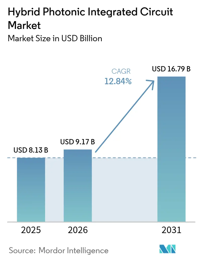
| Market Size (2026) | USD 9.17 Billion |
| Market Size (2031) | USD 16.79 Billion |
| Growth Rate (2026 - 2031) | 12.84% CAGR |
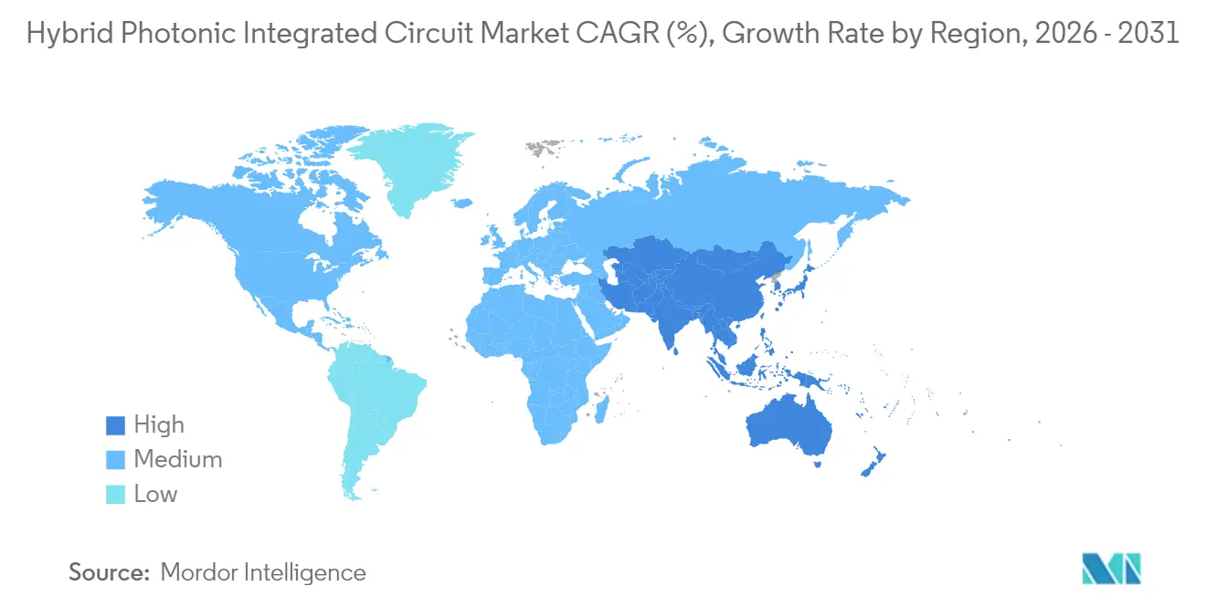
| Fastest Growing Market | Asia Pacific |
| Largest Market | North America |
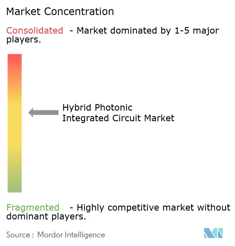
| Market Concentration | Medium |
Major Players *Disclaimer: Major Players sorted in no particular order Image © Mordor Intelligence. Reuse requires attribution under CC BY 4.0. | |
Hybrid Photonic Integrated Circuit Market Analysis by Mordor Intelligence
The Hybrid Photonic Integrated Circuit market size is expected to grow from USD 8.13 billion in 2025 to USD 9.17 billion in 2026 and is forecast to reach USD 16.79 billion by 2031 at 12.84% CAGR over 2026-2031.
Robust demand for co-packaged optics in AI training clusters, the rapid refresh of hyperscale spine fabrics to 800 gigabit and 1.6 terabit rates, and the cost crossover of silicon-III-V heterointegration underpin this expansion. Early volume shipments of optical chiplets have reduced module footprints by 40%, lowered latency to below 10 nanoseconds, and decreased power draw by 30%.[1]Ayar Labs, “Series D Funding and TeraPHY Milestones,” Ayar Labs, ayarlabs.com Public funding in China, Taiwan, and the United States secures the construction of new 300 millimeter photonics fabs, while thin-film lithium niobate modulators enable lower-voltage coherent links for long-haul and quantum applications. Supply remains tight because only five qualified foundries currently bond III-V dies at commercial yield, allowing integrated device manufacturers to maintain pricing power.
Key Report Takeaways
- By application, datacom and cloud interconnect led with 46.05% revenue share in 2025; high-performance computing and AI accelerators segment is forecast to expand at a 13.98% CAGR through 2031.
- By material platform, silicon-III-V hybrid devices held 58.05% of the hybrid photonic integrated circuit market share in 2025, while thin-film lithium niobate is projected to grow at a 14.22% CAGR to 2031.
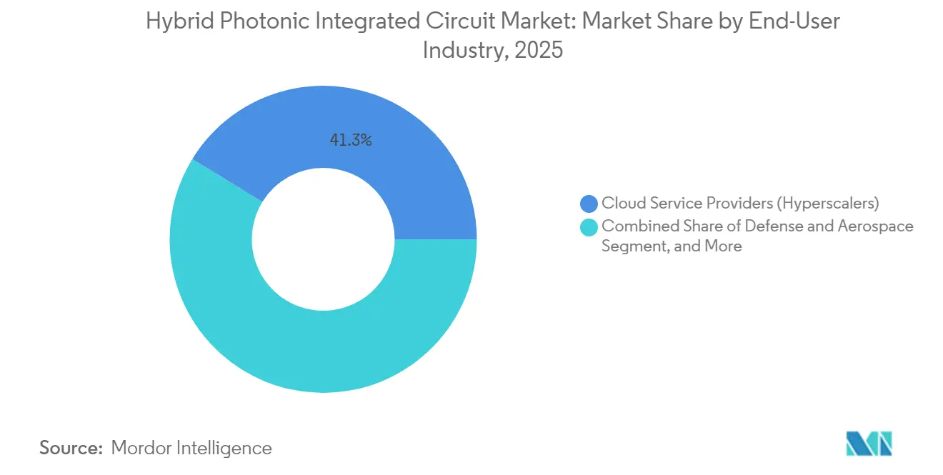
- By end-user industry, cloud service providers accounted for 41.25% of 2025 revenue; the defense and aerospace sector shows the fastest growth with a 13.46% CAGR through 2031.
- By geography, North America accounted for 38.10% in 2025, while the Asia-Pacific region is on track for a 13.55% regional CAGR between 2026 and 2031.
Note: Market size and forecast figures in this report are generated using Mordor Intelligence’s proprietary estimation framework, updated with the latest available data and insights as of 2026.
Global Hybrid Photonic Integrated Circuit Market Trends and Insights
Drivers Impact Analysis*
| Driver | (~) % Impact on CAGR Forecast | Geographic Relevance | Impact Timeline |
|---|---|---|---|
| AI/ML-optimised co-packaged optics demand | +2.8% | North America, Asia-Pacific (China, Taiwan) | Short term (≤ 2 years) |
| Hyperscale datacenter bandwidth explosion | +2.5% | Global, concentrated in North America and Asia-Pacific | Medium term (2-4 years) |
| 5G/6G fronthaul and mid-haul optical densification | +1.9% | Asia-Pacific, Europe, Middle East | Medium term (2-4 years) |
| Silicon + III-V heterointegration cost crossover | +2.1% | Global, early adopters in North America and Taiwan | Long term (≥ 4 years) |
| Defense LiDAR and RF-photonics procurement surge | +1.4% | North America, Europe (NATO), Middle East | Medium term (2-4 years) |
| Emerging chiplet packaging standards (UCIe-P) adoption | +1.6% | Global, led by North America and Asia-Pacific | Long term (≥ 4 years) |
| Source: Mordor Intelligence | |||


AI/ML-Optimised Co-Packaged Optics Demand
Training trillion-parameter models now drives per-rack traffic beyond 400 terabits per second, a threshold that front-panel pluggables cannot meet without prohibitive power loss. Co-packaged optics place photonic dies beside switch ASICs, trimming electrical reach and delivering sub-10-nanosecond hop latency. Meta validated production readiness in its 2024 Grand Teton cluster, while Ayar Labs shipped more than 10,000 optical chiplets and secured 2025 volume ramps. Sovereign-AI rules in Europe and India require local inference, driving mid-scale deployments that necessitate compact optical I/O.[2]European Commission, “European Chips Act,” European Commission, europa.eu Early adopters report a 30% lower interconnect power and a 2-year payback period versus discrete optics, thereby accelerating the adoption curve of the hybrid photonic integrated circuit market.
Hyperscale Datacenter Bandwidth Explosion
Global IP traffic is projected to reach 4.8 zettabytes in 2026, driven by video streaming and the adoption of generative AI.[3]Cisco Systems, “Annual Internet Report 2024-2026,” Cisco, cisco.com Hyperscalers are expected to transition to 800 gigabit Ethernet spines in 2025 and 1.6 terabit optics in 2026, thereby compressing refresh cycles from 5 years to 3 years. Microsoft upgraded 60% of its backbone to 400 gigabit coherent in 2024, cutting cost per bit by 35%. Each speed jump tightens the link budget and favors monolithic photonic-electronic co-design, thereby boosting demand for the hybrid photonic integrated circuit market. Thin-film lithium niobate offers 3 decibels higher efficiency than indium phosphide, enabling lower-voltage 1.6 terabit modules.
5G/6G Fronthaul and Mid-Haul Optical Densification
Centralized radio access splits processing from remote radios, creating low-latency fronthaul lanes that already push 25 gigabit per antenna. China Mobile installed 1.2 million 5G base stations in 2024, each needing two fiber pairs. The 6G roadmap targets 100 gigabit per sector by 2028, steering the industry to coherent detection at cell sites.[4]International Telecommunication Union, “IMT-2030 Framework,” ITU, itu.int Nokia showed a photonic beamforming prototype that slashed antenna complexity by 60%. India’s Bharat 6G Alliance subsidizes up to 50% of photonics capex, accelerating local hybrid photonic integrated circuit market growth. These deployments favor hybrid integration over discrete lasers, sustaining a healthy order pipeline.
Silicon + III-V Heterointegration Cost Crossover
Wafer-scale bonding pushed die cost below USD 50 in 2024, moving hybrid devices under the cost of pure III-V transceivers. Intel’s process adds a single bonding stage that represents less than 15% of total die cost. TSMC’s Songjiang line targets 10,000 wafer starts per month for hybrid dies by 2026, ensuring supply depth in Asia-Pacific. GlobalFoundries shipped over 500,000 Fotonix dies in 2024, tripling 2023 volume. Low-cost polymer waveguides now approach USD 5 per die for short-reach links, although thermal headroom limits adoption above 85 °C.
Restraints Impact Analysis*
| Restraint | (~) % Impact on CAGR Forecast | Geographic Relevance | Impact Timeline |
|---|---|---|---|
| Heterogeneous bonding yield challenges | -0.8% | Global, acute in Asia-Pacific emerging fabs and new entrants outside established foundries | Short term (≤ 2 years) |
| Thermal mismatch reliability issues | -0.6% | Global, critical for defense and aerospace applications and automotive LiDAR deployments | Medium term (2-4 years) |
| Limited ecosystem for hybrid design automation | -0.4% | Global, particularly impacting fabless startups and research institutions | Medium term (2-4 years) |
| Capital-intensive foundry access bottleneck (less than 5 qualified lines) | -0.7% | Global, with supply constraints most severe in Europe and emerging Asia-Pacific markets | Long term (≥ 4 years) |
| Source: Mordor Intelligence | |||
Heterogeneous Bonding Yield Challenges
Bonding III-V dies on 300 millimeter silicon still reaches only 92 to 95% yield, pushing up unit cost by 3-5% per lost point. Tower Semiconductor improved to 94% in Q4 2024 but remains shy of the 98% goal for automotive grade. Void formation during thermal anneal adds up to 2 decibel optical loss and accelerates delamination. Imec’s plasma-activated bonding lowers voids by 70% yet raises process cost by 15%. The limited pool of five qualified foundries acts as a near-term supply cap and restrains the hybrid photonic integrated circuit market until new capacity matures.
Thermal Mismatch Reliability Issues
Silicon and indium phosphide differ in expansion coefficient by 40%, causing stress fractures under -40 to +125 °C cycling. Automotive LiDAR modules demand 15-year life in this envelope SAE.ORG. Defense systems face similar extremes in unpressurized bays and experience 0.5 decibel alignment drift per 1,000 hours. MIT researchers showed a polymer buffer that cuts peak stress by 60%, extending mean time to failure to 25,000 hours at 85 °C. Lumentum now pilots localized laser annealing to reflow adhesives without harming active layers. Thin-film lithium niobate’s low drive voltage lowers thermal load by 30% and gains favor in thermally constrained co-packaged designs
*Our forecasts treat driver/restraint impacts as directional, not additive. The impact forecasts reflect baseline growth, mix effects, and variable interactions.
Segment Analysis
By Application: AI Acceleration Drives Long-Term Upside
High-Performance Computing and AI Accelerators account for the fastest 13.98% CAGR, reflecting surging inter-GPU bandwidth that outstrips electrical SerDes. Datacom and Cloud Interconnect remains the largest slice with 46.05%, supported by the installed base of 100 and 400 gigabit links that migrate to 800 gigabit optics. The hybrid photonic integrated circuit market size for AI accelerators is projected to add more than USD 2.45 billion between 2026 and 2031, driven by sovereign-AI buildouts in Europe and Asia. Telecom backhaul, LiDAR sensing, and RF-photonics retain niche but profitable positions thanks to specialized performance needs.
The shift from centralized training clusters to edge inference pushes optical I/O into servers, smart NICs, and even embedded systems. Meta’s co-packaged deployment cut intra-rack latency under 10 nanoseconds. Automotive LiDAR is moving to 1550-nanometer FMCW designs that integrate tunable lasers and coherent receivers on a single die, reinforcing hybrid adoption. RF-photonics supports a 40-gigahertz instantaneous bandwidth for next-generation radar, meeting defense demand. Healthcare diagnostics enter early trials with lab-on-chip photonics for real-time pathogen detection.


By Material Platform: Lithium Niobate Captures Momentum
Silicon-III-V hybrids retain 58.05% of 2025 revenue on mature epitaxy and gain media, yet lithium niobate now expands at 14.22% CAGR. This trajectory suggests silicon-III-V still dominates the hybrid photonic integrated circuit market share, but lithium niobate’s electro-optic coefficient drives future coherent upgrades. Silicon nitride-III-V architectures appeal to quantum and submarine vendors due to their ultra-low-loss waveguides, while polymer hybrids cater to cost-sensitive consumer devices.
Thin-film lithium niobate enables a π-phase shift of under 2 volts, reducing power consumption by 40% in co-packaged modules. HRL Labs showcased 110 gigahertz bandwidth, lending headroom for 1.6 terabit links. Silicon nitride guides reach 0.1 decibel per centimeter loss and gain traction in entangled photon sources. Polymer photonics hits sub-USD 5 per die but faces thermal limits at 85 °C. Market participants weigh trade-offs between cost, bandwidth, and thermal resilience as application requirements diverge.
By End-User Industry: Defense and Aerospace Accelerate
Cloud Service Providers dominate with 41.25% of 2025 spending, reflecting hyperscaler reliance on co-packaged and pluggable optics. Defense and Aerospace, however, rise at 13.46% CAGR as photonic beamforming and LiDAR move from prototype to procurement. Telecom operators upgrade metro networks to 400 and 800 gigabit coherent, for instance, China Telecom alone ordered 200,000 modules in 2024. Healthcare and industrial automation enter early adoption, each under 5% share today but with expanding venture backing.
Defense users select integrated RF-photonics modules that steer phased-array beams 180 degrees within 1 microsecond, a capability previously unreachable with legacy electronics. Cloud buyers diversify supply by co-investing in domestic photonics startups, lowering geopolitical risk. European carriers consolidate transport layers to cut energy by 25% through coherent photonics. Automotive OEMs, such as Volvo, plan to roll out fleet-wide LiDAR by 2026, cementing another growth pocket.
Geography Analysis
North America held 38.10% of 2025 revenue, buoyed by Intel’s New Mexico fab and Ayar Labs volume shipments. The Federal CHIPS Act grants, totaling USD 1.5 billion, earmark photonics R&D, ensuring local leadership. Cloud builders in the United States fast-track 800 gigabit spines, pulling high-volume demand into domestic fabs. Canada’s quantum photonics programs add specialty orders for silicon nitride waveguides.
Asia-Pacific posts the highest 13.55% CAGR, driven by China’s USD 10 billion foundry stimulus and Taiwan’s advanced packaging clusters. TSMC’s Songjiang pilot line is set to begin hybrid die runs, targeting 10,000 wafers per month by 2026. Japan’s USD 200 million photonics consortium teams Fujitsu and NTT on a 1.6 terabit coherent system, while India’s Semiconductor Mission allocates USD 500 million for local fabs. South-East Asian EMS vendors eye polymer photonics for consumer optics, extending regional supply chains.
Europe benefits from Imec’s multi-project wafer program and the Netherlands’ lithography ecosystem; however, its hybrid photonic integrated circuit market size lags behind that of North America and the Asia-Pacific region. The European Chips Act reserves EUR 500 million for pilot lines focused on heterogeneous bonding and quantum devices. Germany and France direct automotive LiDAR funding, while the U.K. backs silicon photonics for biosensing. Middle East operators like STC install 400 gigabit coherent for metro links, though local manufacturing remains minimal. Africa’s early pilots in South Africa explore silicon photonics for broadband access, setting a foundation for future uptake.

Competitive Landscape
The top five suppliers, Intel, Broadcom, Marvell, Lumentum, and Cisco, command roughly 35% combined revenue, signaling moderate concentration. Incumbents leverage mature III-V epitaxy and supply chains, whereas venture-backed Ayar Labs and Rockley Photonics advance chiplet architectures that bypass conventional module assembly, shortening cycles by 12 months. The hybrid photonic integrated circuit market, therefore, balances scale economies with pockets of agile innovation.
A structural moat surrounds the five foundries capable of commercial heterogeneous bonding: Intel, GlobalFoundries, Tower, TSMC Songjiang, and IMEC. Intel’s 2024 manufacturing pact with Ayar Labs secures optical chiplet capacity for two tier-1 clouds starting in 2025. Broadcom shipped the first 1.6 terabit coherent pluggable that merges DSP and III-V modulators on one die, cutting power 40%.
White-space opportunities include automotive-grade solid-state LiDAR, where only three vendors hold AEC-Q100 approval. Quantum photonics demands silicon nitride waveguides below 0.1 decibel per centimeter loss, a feat fewer than ten foundries can reproduce at scale. The more than 150 lithium niobate modulator patent applications filed in 2024 indicate intensifying competition. The new UCIe-P standard is expected to commoditize optical I/O, enabling multi-vendor ecosystems by 2028.
Hybrid Photonic Integrated Circuit Industry Leaders
Intel Corporation
Broadcom Inc.
Lumentum Holdings
Marvell Technology (Inphi)
Coherent Corp. (II-VI)
- *Disclaimer: Major Players sorted in no particular order

Recent Industry Developments
- October 2024: Intel Corporation announced volume production of co-packaged optics modules at its New Mexico facility, integrating silicon photonics dies directly alongside switch ASICs to achieve sub-10 nanosecond interconnect latency.
- September 2024: Ayar Labs completed a USD 155 million Series D funding round led by Microsoft and Google, bringing total capital raised to USD 370 million. The investment will fund capacity expansion for TeraPHY optical I/O chiplets, with production targets of 100,000 units per quarter by mid-2025.
- August 2024: Broadcom launched its 1.6 terabit coherent pluggable transceiver, featuring a monolithic photonic-electronic co-design that integrates digital signal processors with III-V modulators on a single die. The module reduces power consumption by 40% compared with prior 800 gigabit optics.
- July 2024: TSMC’s Songjiang facility in China began pilot production of silicon-III-V hybrid dies, targeting 10,000 wafer starts per month by mid-2026.


Global Hybrid Photonic Integrated Circuit Market Report Scope
A microchip contains two or more optical components forming a working circuit, which is sometimes referred to as an Integrated Photonics Circuit. This system is capable of detecting, generating, transporting, and processing.
The scope of the study covers photonic ICs, their growth and restricting factors, and the increased demand across various applications. The study also briefly analyzes the impact of macroeconomic trends on the market. The concept of the photonic integrated circuit is similar to electronic integrated circuits.
The photonic integrated circuit market is segmented by type of raw material (iii-v material, lithium niobate, silica-on-silicon, and other raw materials), integration process (hybrid and monolithic), application (telecommunications, biomedical, data centers, and other applications [optical sensors[LiDAR], and metrology]), and geography (North America, Europe, Asia Pacific and the rest of the World). The Market Size and Forecasts are Provided in Terms of Value in USD for all the Above Segments.
| Datacom and Cloud Interconnect |
| Telecom Transport and 5G/6G Mobile Backhaul |
| LiDAR and Optical Sensing |
| High-performance Computing (HPC) and AI Accelerators |
| RF-Photonics and Microwave Photonics |
| Silicon-III-V Hybrid (InP/GaAs on Si) |
| Silicon Nitride-III-V |
| Polymer Photonics Hybrid |
| Thin-film Lithium Niobate on Si |
| Others (SiGe, AlN, etc.) |
| Cloud Service Providers (Hyperscalers) |
| Telecom Operators and Network OEMs |
| Defense and Aerospace |
| Healthcare and Biosensing OEMs |
| Industrial and Automotive OEMs |
| North America | United States |
| Canada | |
| Mexico | |
| Europe | Germany |
| United Kingdom | |
| France | |
| Netherlands | |
| Rest of Europe | |
| Asia-Pacific | China |
| India | |
| Japan | |
| South Korea | |
| ASEAN | |
| Rest of Asia-Pacific | |
| Rest of the World |
| By Application | Datacom and Cloud Interconnect | |
| Telecom Transport and 5G/6G Mobile Backhaul | ||
| LiDAR and Optical Sensing | ||
| High-performance Computing (HPC) and AI Accelerators | ||
| RF-Photonics and Microwave Photonics | ||
| By Material Platform | Silicon-III-V Hybrid (InP/GaAs on Si) | |
| Silicon Nitride-III-V | ||
| Polymer Photonics Hybrid | ||
| Thin-film Lithium Niobate on Si | ||
| Others (SiGe, AlN, etc.) | ||
| By End-user Industry | Cloud Service Providers (Hyperscalers) | |
| Telecom Operators and Network OEMs | ||
| Defense and Aerospace | ||
| Healthcare and Biosensing OEMs | ||
| Industrial and Automotive OEMs | ||
| By Geography | North America | United States |
| Canada | ||
| Mexico | ||
| Europe | Germany | |
| United Kingdom | ||
| France | ||
| Netherlands | ||
| Rest of Europe | ||
| Asia-Pacific | China | |
| India | ||
| Japan | ||
| South Korea | ||
| ASEAN | ||
| Rest of Asia-Pacific | ||
| Rest of the World | ||


Key Questions Answered in the Report
What is driving new demand for hybrid photonic ICs in AI clusters?
Co-packaged optics trim power by 30% and lower latency below 10 nanoseconds, enabling racks that move more than 400 terabits per second.
Which material platform is growing the fastest through 2031?
Thin-film lithium niobate on silicon leads with a 14.22% CAGR thanks to low-voltage, high-bandwidth modulators.
Why is Asia-Pacific expanding quicker than other regions?
China’s USD 10 billion foundry program and Taiwan’s advanced packaging ecosystem push the region to a 13.55% CAGR.
How concentrated is supply of heterogeneous bonding capacity?
Only five commercial foundries hold qualified processes, creating a structural bottleneck and sustaining pricing power.
What segments offer the highest growth beside hyperscale datacenters?
Defense LiDAR and RF-photonics rise at 13.46% CAGR as programs shift from prototype to volume procurement.
Page last updated on:


