
GPU Wafer Demand Market Size and Share
Market Overview
| Study Period | 2020 - 2031 |
|---|---|
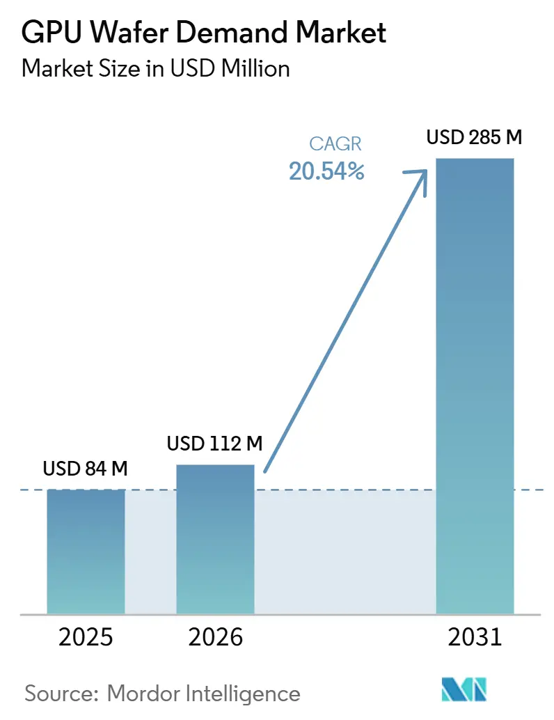
| Market Size (2026) | USD 112 Million |
| Market Size (2031) | USD 285 Million |
| Growth Rate (2026 - 2031) | 20.54 % |
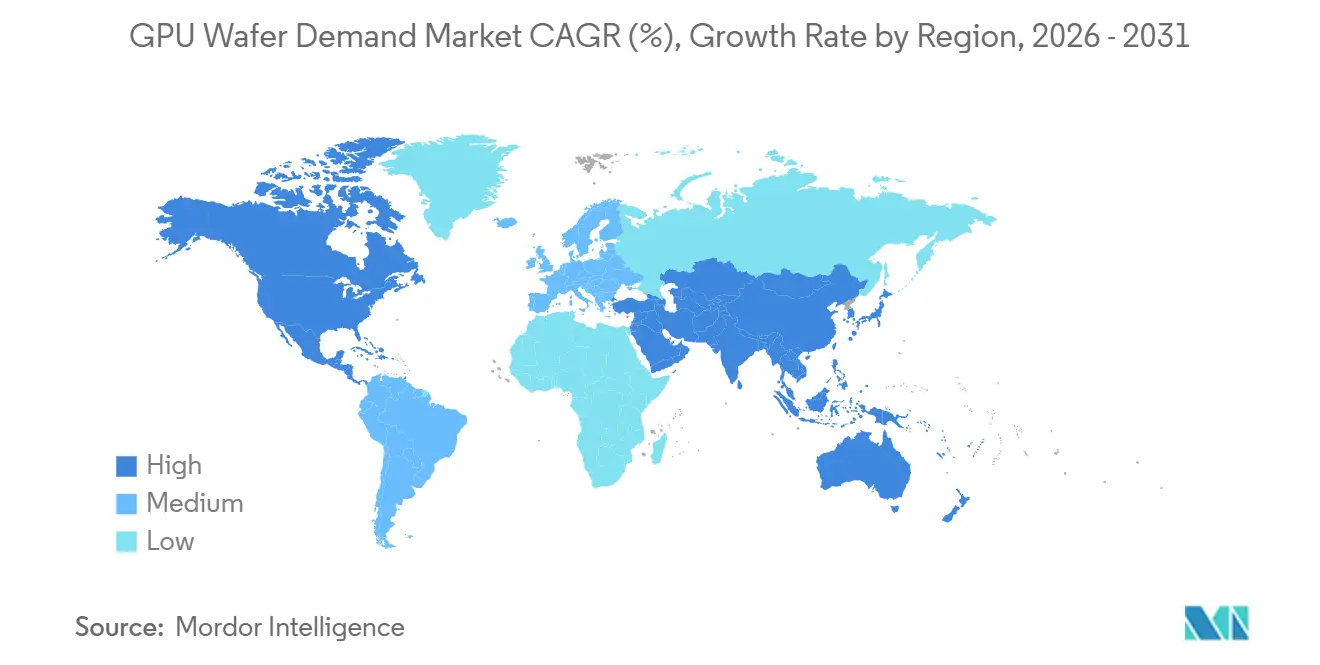
| Fastest Growing Market | North America |
| Largest Market | Asia-Pacific |
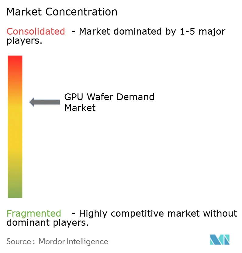
| Market Concentration | Medium |
Major Players *Disclaimer: Major Players sorted in no particular order Image © Mordor Intelligence. Reuse requires attribution under CC BY 4.0. | |
GPU Wafer Demand Market Analysis by Mordor Intelligence
The GPU wafer demand market size is expected to increase from USD 84.00 million in 2025 to USD 112.00 million in 2026 and reach USD 285.00 million by 2031, growing at a CAGR of 20.54% over 2026-2031. The GPU wafer demand market covers the value of silicon substrates used only in GPU fabrication, which makes it a small but strategically important part of the wider silicon materials space. Demand is now tied more closely to AI accelerator procurement than to legacy gaming cycles, because hyperscalers are building long planning windows for training and inference capacity. As process technology moves deeper into advanced nodes, wafer specifications become stricter, which raises value per substrate even when physical area growth remains measured. Supply conditions are also shaped by a highly concentrated vendor base and by long contract periods, which keep most advanced material locked into pre-qualified customer channels. That combination of AI-led demand, specification intensity, supply concentration, and localization incentives keeps the GPU wafer demand market positioned for strong expansion through 2031.
Key Report Takeaways
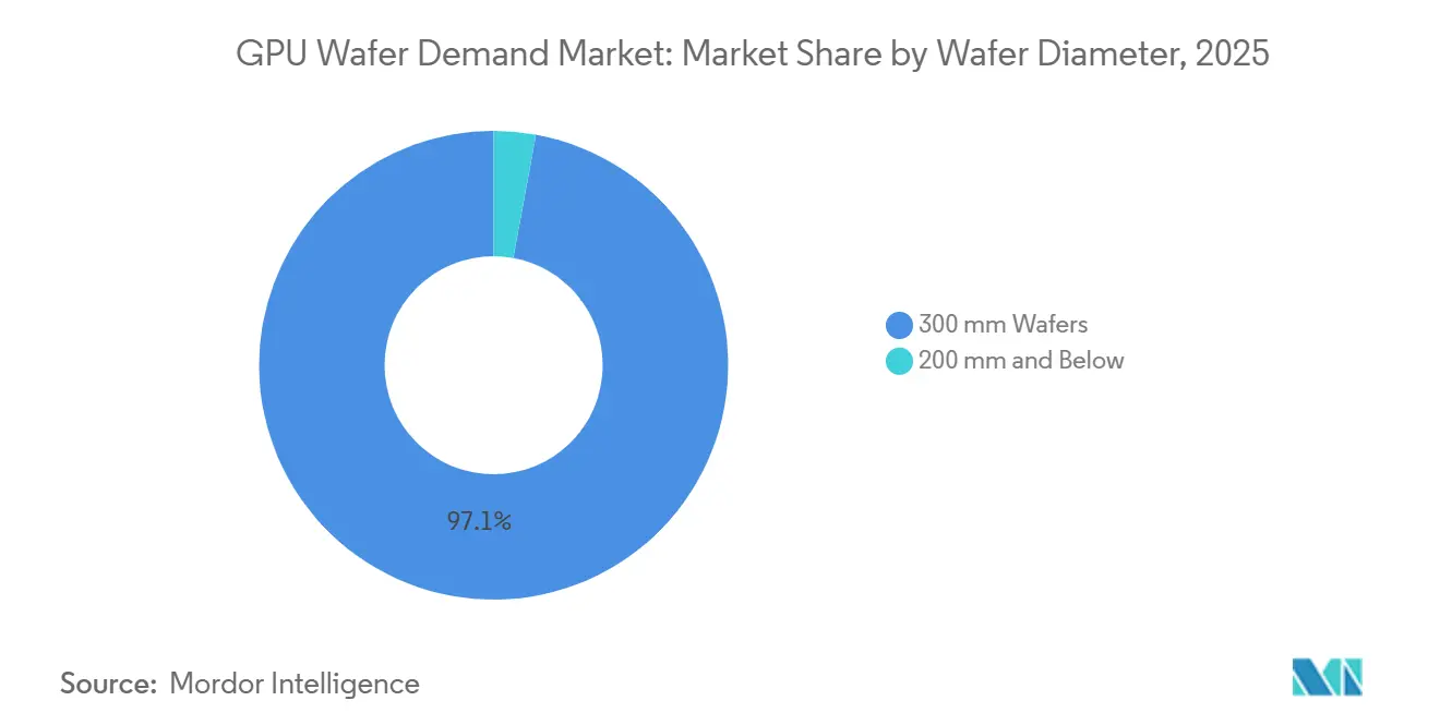
- By wafer diameter, 300 mm wafers held 97.11% of GPU wafer demand market share in 2025, and the same segment is projected to expand at a 21.21% CAGR through 2031.
- By starting wafer type, prime polished bulk silicon wafers held 82.33% share in 2025, while epitaxial silicon wafers are projected to grow at a 21.62% CAGR through 2031.
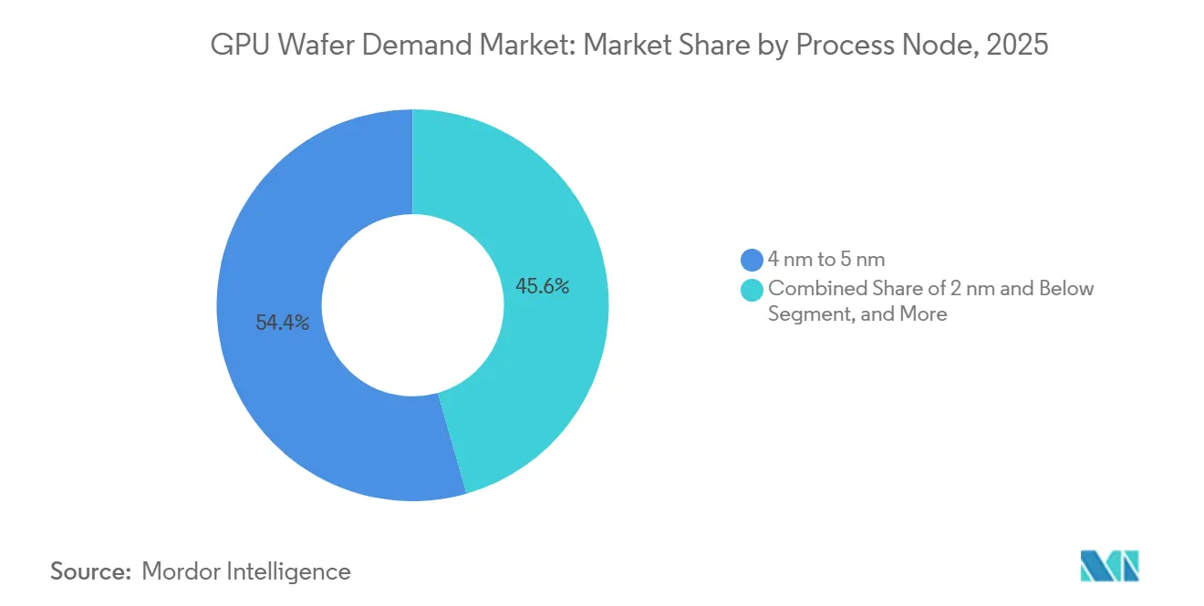
- By process node, the 4 nm to 5 nm category accounted for 54.42% share of the GPU wafer demand market size in 2025, while the 2 nm and below category is projected to advance at a 21.53% CAGR through 2031.
- By GPU application, data center and AI/HPC GPUs accounted for 73.12% share of the GPU wafer demand market size in 2025, and the same segment is projected to grow at a 21.32% CAGR through 2031.
- By geography, Asia-Pacific retained 86.44% share in 2025, while North America is projected to expand at a 21.42% CAGR through 2031.
Note: Market size and forecast figures in this report are generated using Mordor Intelligence’s proprietary estimation framework, updated with the latest available data and insights as of January 2026.
Market Trends and Insights
Drivers Impact Analysis of GPU Wafer Demand Market*
| Driver | (~) % Impact on CAGR Forecast | Geographic Relevance | Impact Timeline |
|---|---|---|---|
| AI Training Density Raises Ultra-Low Defect Wafer Requirements | +4.5% | Global, highest concentration in Asia-Pacific, especially Taiwan and South Korea | Medium term (2-4 years) |
| 3 nm and 2 nm GPU Ramps Increase Prime Wafer Pull | +3.8% | Asia-Pacific core, with spillover to North America through Arizona expansion | Long term (≥ 4 years) |
| Backside Power Delivery Increases Epitaxial Specification Intensity | +2.9% | Global, with near-term emphasis on Taiwan and South Korea | Medium term (2-4 years) |
| Localization Incentives Re-Shape Strategic Wafer Procurement | +2.4% | North America, Europe, and Japan | Short term (≤ 2 years) |
| Chiplet-Based GPU Architectures Expand SOI and Specialty Wafer Demand | +1.8% | Global, with SOI supply centered in France and the United States | Long term (≥ 4 years) |
| Sustainability Programs Accelerate Reclaimed Wafer Adoption in R&D | +0.8% | Global, mainly North America and Europe | Long term (≥ 4 years) |
| Source: Mordor Intelligence | |||
AI Training Density Raises Ultra-Low Defect Wafer Requirements
The GPU wafer demand market is being pushed higher by the physical intensity of AI training, because very large compute die are less tolerant of even small variations in surface quality and defect control. That makes wafer quality a direct cost issue for foundries and GPU vendors, since small yield losses at advanced nodes can erase large amounts of output value. Shin-Etsu said AI chips for GPUs and high-bandwidth memory accounted for just under 10% of total 300 mm wafer demand, while broader AI-related end markets, including data centers and servers, exceeded 20% of total 300 mm demand in the fiscal year ended March 2026.[1] As that mix rises, suppliers that can consistently deliver ultra-flat and low-defect substrates gain stronger pricing power and a more protected position inside advanced qualification programs. The GPU wafer demand market therefore rewards wafer makers that can work closely with foundries on defect budgets and process control, because those relationships are likely to carry forward across multiple node transitions.
3 nm and 2 nm GPU Ramps Increase Prime Wafer Pull
The GPU wafer demand market is also rising as leading GPU programs move into smaller process nodes that require more exacting substrate performance and tighter production planning. This shift matters not only because node migration improves chip capability, but also because it raises the commercial value of each qualified wafer start inside advanced logic lines. SUMCO reported that 300 mm wafer shipments grew 9% in 2025, led by leading-edge logic and high-bandwidth memory demand tied to AI, which marked a clear recovery from the weaker conditions seen earlier in the cycle.[2] SUMCO also said AI-use DRAM wafer demand is expected to rise from 500,000-600,000 wafers per month currently to 1,500,000 wafers per month over the next 3-4 years, which shows how tightly AI compute growth is now linked to upstream silicon requirements. In the GPU wafer demand market, that node migration strengthens demand for prime 300 mm material and narrows the room for lower-specification suppliers that cannot serve advanced production ramps at scale.
Backside Power Delivery Increases Epitaxial Specification Intensity
The GPU wafer demand market is moving toward more specialized engineered substrates as next-generation device structures place more stress on resistivity control, thickness management, and contamination limits. Backside power delivery is part of that direction, because it shifts more of the performance burden onto wafer properties that were less commercially decisive in earlier GPU generations. Even where prime polished wafers still dominate current volume, advanced customer roadmaps are creating more room for epitaxial and other higher-specification starting material inside the GPU wafer demand market. Soitec’s fiscal year 2026 results showed that Edge and Cloud AI revenue reached EUR 214 million, or USD 225 million, and that Photonics-SOI revenue exceeded USD 100 million, which signals stronger demand for advanced engineered silicon tied to AI infrastructure.[3] The result is a market that is no longer driven only by wafer volume, but also by a deeper mix shift toward material platforms that support tighter electrical and structural performance in advanced GPU designs.
Localization Incentives Re-Shape Strategic Wafer Procurement
The GPU wafer demand market is being reshaped by localization policy, because governments now treat advanced silicon supply as a strategic input rather than as a standard traded material. The US Department of Commerce awarded GlobalWafers USD 406 million under the CHIPS and Science Act, supporting the Sherman, Texas project and a Missouri SOI facility, which marks a direct federal effort to build local wafer capability. NVIDIA also said in 2026 that it and its partners aim to produce up to USD 500 billion of AI infrastructure in the United States, creating a stronger domestic demand anchor for advanced substrate supply over time. For the GPU wafer demand market, that means procurement is slowly splitting into sovereign-preference corridors where resilience, political alignment, and customer proximity matter more than they did in the earlier Asia-centered model. This does not remove Asia-Pacific’s lead, but it does create new openings for qualified suppliers that can match domestic policy support with reliable advanced-node execution.
Restraints Impact Analysis of GPU Wafer Demand Market*
| Restraint | (~) % Impact on CAGR Forecast | Geographic Relevance | Impact Timeline |
|---|---|---|---|
| High-Purity Polysilicon Supply Limits 300 mm Output | -1.8% | Global, most acute in North America and Europe | Medium term (2-4 years) |
| Long GPU Customer Qualification Cycles Delay Supplier Switching | -1.4% | Global | Long term (≥ 4 years) |
| Float-Zone and Prime Wafer Capex Raises Entry Barriers | -0.8% | Global | Long term (≥ 4 years) |
| Export Controls on Advanced Node Equipment Slow China Expansion | -0.7% | China-specific, with spillover to global supply through restricted capacity build | Medium term (2-4 years) |
| Source: Mordor Intelligence | |||
High-Purity Polysilicon Supply Limits 300 mm Output
The GPU wafer demand market faces a real supply restraint from electronic-grade polysilicon, because advanced wafer production depends on very high purity feedstock that is not easily replaced by lower-grade material. The Semiconductor Industry Association told the US Department of Commerce in August 2025 that import dependence across key silicon inputs and wafer products remains a strategic weakness for domestic semiconductor expansion. USGS also confirmed that 3 companies produced polysilicon in the United States in 2025, while a 4th ceased production after failing to meet customer quality and volume standards, which reduced domestic flexibility at the same time that advanced-node demand kept rising. That tightness matters for the GPU wafer demand market because wafer capacity cannot expand smoothly when feedstock quality, rather than only fab equipment, becomes the limiting step. Until new qualified supply reaches commercial scale, premium 300 mm substrates are likely to remain supported by a firm pricing floor and limited availability.
Long GPU Customer Qualification Cycles Delay Supplier Switching
The GPU wafer demand market remains difficult for new entrants because qualification cycles are long, expensive, and closely tied to customer-specific process control. Once a wafer supplier is approved for a given foundry flow, switching becomes unattractive during an active production ramp because it requires renewed work on reliability, metrology correlation, and yield stability. That creates a strong installed advantage for incumbent vendors across the GPU wafer demand market, even when new capacity is built elsewhere. The CHIPS-linked expansion cycle in the United States shows this clearly, because local production assets can be funded faster than customer qualification can be completed across advanced supply chains. The practical result is that capacity additions help long-run resilience, but they do not quickly open the market to broad supplier substitution during the current AI-led demand cycle.
*Our forecasts treat driver/restraint impacts as directional, not additive. The impact forecasts reflect baseline growth, mix effects, and variable interactions.
GPU Wafer Demand Market Segment Analysis
By Wafer Diameter:
300 mm Substrate Concentration Reflects Advanced GPU Node Economics300 mm wafers held 97.11% of GPU wafer demand market share in 2025, and the segment is projected to grow at a 21.21% CAGR from 2026 to 2031. That dominance reflects economics as much as technology, because advanced GPU production simply cannot be scaled efficiently on smaller formats once die complexity, process precision, and output value all move higher. The GPU wafer demand market therefore remains centered on the 300 mm platform, while 200 mm and below mostly serve legacy gaming, embedded, and edge products built on older nodes. This split is structural rather than temporary, since the smaller-diameter category has limited relevance for the leading AI accelerators that now shape most forward purchasing decisions. In practical terms, the GPU wafer demand industry has already settled around a format hierarchy where 300 mm captures nearly all advanced value creation.
The 300 mm segment also has an outsized influence on pricing, because nearly every major supply bottleneck in advanced logic now runs through qualified 300 mm lines and their associated materials ecosystem. Demand concentration in that format supports long contract periods, disciplined capacity additions, and stronger bargaining power for suppliers that already hold advanced customer approvals. The GPU wafer demand market is therefore more exposed to 300 mm utilization, qualification status, and regional capacity location than to total wafer unit counts alone. Smaller diameters still matter for some niche and cost-sensitive programs, but they do not shape the revenue base of the GPU wafer demand market in the same way. This is why new investment announcements from leading suppliers continue to target advanced 300 mm output rather than broad-based expansion across all diameter classes.
By Starting Wafer Type:
Epitaxial Wafers Emerge as AI Node EnablersPrime polished bulk silicon wafers held 82.33% share of 2025 demand, while epitaxial silicon wafers are projected to expand at a 21.62% CAGR from 2026 to 2031. Prime polished substrates remain the working base for large volumes of current GPU production because they fit the needs of established 4 nm to 7 nm programs without requiring a full shift toward more engineered starting material. Even so, the GPU wafer demand market is gradually moving toward a richer mix of epitaxial and other engineered wafers as tighter electrical performance and process control requirements spread across advanced designs. This shift matters because it raises the value of materials expertise, not only the value of raw wafer volume. It also raises the competitive threshold for suppliers, since they need stronger control over contamination, resistivity, and uniformity to participate in next-wave qualifications.
The smallest starting wafer categories remain limited in share, but their strategic role is rising as AI systems place more value on specialty material stacks and optical interconnect support. Soitec said Edge and Cloud AI revenue reached EUR 214 million, or USD 225 million, in fiscal year 2026, and Photonics-SOI revenue exceeded USD 100 million earlier than expected, which shows that engineered silicon has become more important inside AI infrastructure spending. In the GPU wafer demand market, this means the largest segment still rests with prime polished bulk silicon, but growth leadership is shifting toward substrates that help support next-generation architecture and packaging needs. The GPU wafer demand industry is therefore becoming more specification-led, with starting wafer choice increasingly linked to system-level design requirements rather than to legacy volume habits. That progression gives epitaxial wafers a clearer path to premium growth through the forecast period.
By Process Node:
Sub-5 nm Nodes Command Premium Wafer AllocationThe 4 nm to 5 nm process node accounted for 54.42% share of the GPU wafer demand market size in 2025, while the 2 nm and below category is projected to grow at a 21.53% CAGR from 2026 to 2031. The present mix shows that advanced but already-established nodes still carry most production weight, because they offer a workable balance between performance, yield learning, and commercial scale. At the same time, the GPU wafer demand market is clearly moving toward smaller geometries as AI workloads continue to favor higher compute density and tighter power efficiency. That node transition supports premium wafer allocation because each successful advanced-node ramp depends on stricter substrate quality and narrower process tolerances. It also strengthens foundry and material supplier interdependence, since the cost of any qualification failure rises sharply as node complexity moves deeper.
The 6 nm to 7 nm and 8 nm to 16 nm bands continue to serve lower-margin or more specialized GPU tasks, including automotive and edge inference programs that do not need the full performance envelope of leading AI accelerators. Nodes above 16 nm still retain a role for support functions inside multi-chip packages, especially where input-output, interface, or power-related functions can remain on older geometries. Even so, the revenue center of gravity in the GPU wafer demand market will continue moving toward sub-5 nm and then toward 2 nm-class programs, because that is where the highest-value GPU deployments are concentrating. The GPU wafer demand market also becomes more sensitive to node mix than to simple unit growth, since smaller geometries increase the commercial weight of every qualified wafer. This is why suppliers that can meet the needs of leading-edge node transitions are positioned to capture a larger share of incremental value than those focused mainly on mature process categories.

By GPU Application:
Data Center and AI/HPC GPUs Anchor the Demand BaseData center and AI/HPC GPUs accounted for 73.12% share of the GPU wafer demand market size in 2025, and the same segment is projected to grow at a 21.32% CAGR from 2026 to 2031. That combination, where the largest application is also the fastest-growing, shows that current expansion is not being driven by a short-lived consumer cycle. Instead, the GPU wafer demand market is being led by sustained buildouts in training clusters, inference infrastructure, and the broader data center systems that support large AI models. This changes procurement behavior because enterprise and hyperscale buyers plan around availability, qualification, and long supply commitments rather than around seasonal refresh patterns. It also helps explain why upstream wafer demand has become more visible and more tightly managed than during earlier gaming-led demand periods.
Gaming and consumer discrete GPUs still hold the second-largest application position, but their role in the GPU wafer demand market is becoming more selective and more weighted toward premium products. Professional visualization and workstation products continue to draw steady wafer allocation because simulation, design, and AI-assisted content tools still require dedicated compute performance. Automotive, embedded, and edge GPUs form the fastest-growing non-datacenter category, though they start from a much smaller base and follow different qualification and pricing logic. Shin-Etsu said broader AI-related demand, including data centers and servers, exceeded 20% of total 300 mm wafer demand, which reinforces the upstream shift toward data center-led silicon consumption. For the GPU wafer demand market, that means application mix now matters as much as total volume, because data center deployments carry stronger pull on advanced wafer specifications, contract duration, and supplier prioritization.
Geography Analysis
APAC GPU Wafer Demand Market
Asia-Pacific retained 86.44% of GPU wafer demand market share in 2025, which keeps the regional base of the GPU wafer demand market heavily concentrated around Taiwan, South Korea, and Japan. This position reflects the fact that advanced GPU fabrication remains centered in Taiwan, while South Korea supports key memory and foundry capacity and Japan anchors a large share of upstream wafer supply. Japan’s Shin-Etsu Handotai and SUMCO together hold over 60% of global 300 mm silicon wafer supply, which gives the region a strong materials advantage close to leading fabrication clusters. SUMCO’s first-quarter 2026 guidance also confirmed continued strength in advanced logic and DRAM wafers for AI data centers, even as non-advanced products and 200 mm formats remained softer. Shin-Etsu further said broader AI-related wafer demand exceeded 20% of total 300 mm demand and that growth from April to June 2026 was expected to outpace earlier projections, which supports the region’s lead in the current cycle.
North America GPU Wafer Demand Market
North America is projected to grow at a 21.42% CAGR from 2026 to 2031, making it the fastest-rising geography in the GPU wafer demand market. The main driver is policy-backed localization, because federal incentives are now aligned with domestic semiconductor and AI infrastructure expansion. The US Department of Commerce award to GlobalWafers supports the first advanced high-volume 300 mm silicon wafer manufacturing platform in the United States in more than 20 years, which gives the region a clearer path toward local substrate availability. NVIDIA’s 2026 commitment to build up to USD 500 billion of AI infrastructure in the United States with partners including TSMC, Foxconn, and Corning adds a strong demand-side signal for domestic supply chain development. Even so, the GPU wafer demand market in North America will still need time to align customer qualification, foundry schedules, and local materials output before the full benefit appears.
EMEA and South America GPU Wafer Demand Market
Europe holds a smaller direct position in volume, but it remains relevant through specialized supplier capabilities and balance-sheet support for 300 mm expansion. Siltronic raised EUR 273 million, or USD 298 million, in June 2026 to support its long-term 300 mm growth strategy, which points to continued confidence in advanced silicon demand. Soitec also strengthened Europe’s position in high-value niches by reporting Photonics-SOI revenue above USD 100 million in fiscal year 2026, which ties the region more closely to optical and engineered silicon roles in AI systems. South America and the Middle East and Africa remain peripheral to the GPU wafer demand market in 2026, with activity focused more on downstream electronics and future sovereign AI spending than on upstream wafer manufacturing. The overall regional picture therefore remains clear, because Asia-Pacific still leads in scale, North America is building the fastest new growth path, and Europe is defending a focused position in specialty and advanced materials.
Competitive Landscape
The GPU wafer demand market remains highly consolidated, with Shin-Etsu Handotai, SUMCO, GlobalWafers, Siltronic, and SK Siltron together accounting for over 90% of qualified 300 mm silicon supply. The Semiconductor Industry Association described concentration and import dependence in silicon materials as a strategic vulnerability in its August 2025 Section 232 submission, which highlights how narrow the qualified supplier base remains. In the GPU wafer demand market, that structure gives incumbents strong protection because customer qualification, process correlation, and advanced capacity are difficult to replicate quickly. It also means pricing and supply access are influenced less by open-market competition and more by contract position, technical approval status, and physical proximity to major foundry ecosystems. This is a market where scale matters, but qualification depth matters even more.
The leading companies are not following one single expansion model. Shin-Etsu said it planned approximately JPY 350 billion (USD 2.24 billion), in capital expenditure for the fiscal year ending March 2027, with spending directed toward semiconductor wafer and AI-related materials capacity. GlobalWafers is using the localization route, supported by CHIPS funding for the Sherman, Texas campus, which gives it a clearer role in the emerging domestic US wafer base. Siltronic is reinforcing its balance sheet and 300 mm growth strategy through fresh capital, while Soitec continues to deepen its position in engineered silicon and photonics for AI-linked use cases. The GPU wafer demand market therefore shows a split strategy, where some leaders invest deeper in home-country process upgrades and others invest in geography-based resilience and customer access.
Smaller and emerging challengers remain active, but their near-term effect on the GPU wafer demand market is limited by qualification barriers and by the dominance of long-established supplier relationships. Chinese companies are expanding 12-inch capability to reduce import dependence, yet they still face a slower path into the most advanced GPU flows because leading foundries require extended validation and repeatable process data. Western niche players can defend positions in float-zone, high-resistivity, or specialty engineered substrates, but they do not yet match the scale and breadth of the main 300 mm leaders. Soitec’s first delivery of custom silicon-28 enriched FD-SOI wafers for quantum processing at STMicroelectronics’ 300 mm facility in Crolles, France, also shows that adjacent high-value applications can strengthen supplier positioning without directly competing on commodity volume. As a result, the GPU wafer demand market is likely to remain dominated by the current leaders through the forecast period, with competition focused on capability depth, regional footprint, and strategic specialization rather than on broad-based share disruption.
GPU Wafer Demand Industry Leaders
-
Shin-Etsu Handotai Co., Ltd.
-
SUMCO Corporation
-
Siltronic AG
-
GlobalWafers Co., Ltd.
-
SK Siltron Co., Ltd.
- *Disclaimer: Major Players sorted in no particular order
GPU Wafer Demand Market Companies Covered in this Report
- Shin-Etsu Handotai Co., Ltd.
- SUMCO Corporation
- Siltronic AG
- GlobalWafers Co., Ltd.
- SK Siltron Co., Ltd.
- Soitec S.A.
- Wafer Works Corporation
- Shanghai Simgui Technology Co., Ltd.
- Okmetic Oyj
- Ferrotec Holdings Corporation
- Hangzhou Silicon Tech Co., Ltd.
- Zhonghuan Semiconductor Co., Ltd.
- POSCO Future M Co., Ltd.
- Episil-Precision Inc.
- MEMC Korea Company
- Korea Silicon Wafer Co., Ltd.
- Linton Crystal Technologies
- Salem Advanced Materials Inc.
- Noel Technologies
- Topsil GlobalWafers
Recent Industry Developments in GPU Wafer Demand Market
- June 2026: Siltronic AG successfully completed an accelerated bookbuilding placing of new shares at EUR 91 per share, raising gross proceeds of EUR 273 million (USD 298 million) to support its 300 mm long-term growth strategy and strengthen its balance sheet. The placement was significantly oversubscribed, with anchor shareholder HAL Trust participating. Siltronic confirmed that AI-driven end markets are "clearly supporting" 300 mm volume in 2026, providing the strategic rationale for the raise.
- May 2026: Soitec's fiscal year 2026 full-year results confirmed that Photonics-SOI revenue surpassed USD 100 million, earlier than initially anticipated, as structural adoption of silicon photonics optical interconnects in AI data center co-packaged optics architectures accelerated. Edge and Cloud AI segment revenue reached EUR 214 million (USD 225 million), up 19% year-on-year excluding the phased-out Imager-SOI line. Combined FD-SOI and Photonics-SOI AI-enabler revenues delivered a 25% year-on-year increase.
- April 2026: Shin-Etsu Chemical's earnings for fiscal year ending March 2026 confirmed a capital expenditure plan of approximately JPY 350 billion (USD 2.24 billion) for the current fiscal year, focused on semiconductor wafer and AI-related materials capacity. Management signaled stronger-than-anticipated order momentum from the April to June 2026 quarter, attributed to semiconductor inventory restocking driven by Middle East supply-chain concerns.
- January 2026: GlobalWafers commenced Phase 2 of its 300 mm silicon wafer manufacturing facility in Sherman, Texas, as part of a total planned investment of USD 7.5 billion. Receiving USD 406 million in CHIPS Act federal grants, the Sherman campus, designed to accommodate up to 6 production phases, is the first advanced high-volume 300 mm silicon wafer operation in the United States in over 20 years, directly supporting domestic GPU supply chain security for TSMC Arizona customers.
Global GPU Wafer Demand Market Report Scope
The GPU Wafer Demand Market refers to the industry segment that tracks and analyzes the worldwide demand for semiconductor wafers used in the fabrication of Graphics Processing Units (GPUs), which are critical components for high-performance computing, artificial intelligence (AI), machine learning (ML), gaming, visualization, and data center applications.
The GPU Wafer Demand Market Report is Segmented by Wafer Diameter (300 mm Wafers and 200 mm and Below), Starting Wafer Type (Prime Polished Bulk Silicon Wafers, Epitaxial Silicon Wafers, and SOI and Other Engineered Silicon Wafers), Process Node (2 nm and Below, 3 nm, 4 nm to 5 nm, 6 nm to 7 nm, 8 nm to 16 nm, and Above 16 nm), GPU Application (Data Center and AI/HPC GPUs, Gaming and Consumer Discrete GPUs, Professional Visualization and Workstation GPUs, and Automotive, Embedded, and Edge GPUs), and Geography (North America, Europe, Asia-Pacific, South America, and Middle East and Africa). The Market Forecasts are Provided in Terms of Value (USD).
Segmentation Overview
| 300 mm Wafers |
| 200 mm and Below |
| Prime Polished Bulk Silicon Wafers |
| Epitaxial Silicon Wafers |
| SOI and Other Engineered Silicon Wafers |
| 2 nm and Below |
| 3 nm |
| 4 nm to 5 nm |
| 6 nm to 7 nm |
| 8 nm to 16 nm |
| Above 16 nm |
| Data Center and AI/HPC GPUs |
| Gaming and Consumer Discrete GPUs |
| Professional Visualization and Workstation GPUs |
| Automotive, Embedded, and Edge GPUs |
| North America | United States |
| Canada | |
| Mexico | |
| Europe | Germany |
| United Kingdom | |
| France | |
| Italy | |
| Rest of Europe | |
| Asia-Pacific | China |
| Japan | |
| South Korea | |
| India | |
| Southeast Asia | |
| Rest of Asia-Pacific | |
| South America | |
| Middle East and Africa |
| By Wafer Diameter | 300 mm Wafers | |
| 200 mm and Below | ||
| By Starting Wafer Type | Prime Polished Bulk Silicon Wafers | |
| Epitaxial Silicon Wafers | ||
| SOI and Other Engineered Silicon Wafers | ||
| By Process Node | 2 nm and Below | |
| 3 nm | ||
| 4 nm to 5 nm | ||
| 6 nm to 7 nm | ||
| 8 nm to 16 nm | ||
| Above 16 nm | ||
| By GPU Application | Data Center and AI/HPC GPUs | |
| Gaming and Consumer Discrete GPUs | ||
| Professional Visualization and Workstation GPUs | ||
| Automotive, Embedded, and Edge GPUs | ||
| By Geography | North America | United States |
| Canada | ||
| Mexico | ||
| Europe | Germany | |
| United Kingdom | ||
| France | ||
| Italy | ||
| Rest of Europe | ||
| Asia-Pacific | China | |
| Japan | ||
| South Korea | ||
| India | ||
| Southeast Asia | ||
| Rest of Asia-Pacific | ||
| South America | ||
| Middle East and Africa | ||
Key Questions Answered in the Report
What is the current and forecast value of GPU wafer demand?
The GPU wafer demand market stands at USD 112.00 million in 2026 and is forecast to reach USD 285.00 million by 2031, growing at a 20.54% CAGR over 2026-2031.
What is driving wafer demand for GPUs the most right now?
AI infrastructure is the main driver, especially data center training and inference deployments that are increasing the need for advanced 300 mm substrates and tighter wafer specifications.
Which wafer diameter dominates GPU production?
300 mm wafers led with 97.11% share in 2025, reflecting the fact that advanced GPU fabrication is concentrated on leading-node production economics.
Why are epitaxial wafers gaining importance in advanced GPU manufacturing?
Epitaxial wafers are projected to grow at a 21.62% CAGR because advanced device structures need tighter control over resistivity, contamination, and substrate uniformity.
Which application accounts for most wafer consumption in this space?
Data center and AI/HPC GPUs held 73.12% share in 2025 and are also the fastest-growing application segment with a 21.32% CAGR through 2031.
Which region is growing fastest in GPU wafer demand?
North America is the fastest-growing region at a 21.42% CAGR through 2031, supported by CHIPS-linked localization and expanding domestic AI infrastructure plans.